

Page 1
Any and all SANYO products described or contained herein do not have specifications that can handle
applications that require extremely high levels of reliability, such as life-support systems, aircraft’s
control systems, or other applications whose failure can be reasonably expected to result in serious
physical and/or material damage. Consult with your SANYO representative nearest you before using
any SANYO products described or contained herein in such applications.
SANYO assumes no responsibility for equipment failures that result from using products at values that
exceed, even momentarily, rated values (such as maximum ratings, operating condition ranges,or other
parameters) listed in products specifications of any and all SANYO products described or contained
herein.
Monolithic Linear IC
Audio Level Sensor
Ordering number:ENN1343D
LA2010
SANYO Electric Co.,Ltd. Semiconductor Company
TOKYO OFFICE Tokyo Bldg., 1-10, 1 Chome, Ueno, Taito-ku, TOKYO, 110-8534 JAPAN
Overview
The LA2010 is an IC for detecting interprogram spaces to
pick out the starting point of a program immediately preceding or following musical program recorded on tape.
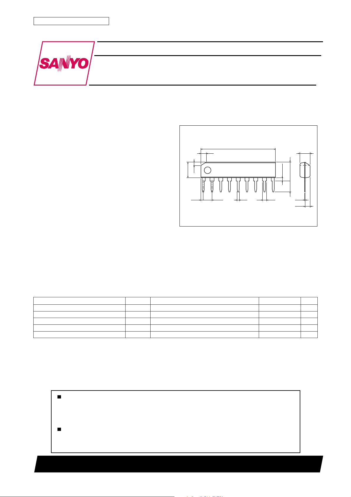
Package Dimensions
unit:mm
3017C-SIP9
[LA2010]
Applicable Sets
• Radio-cassette recorders.
• Cassette decks.
• Car stereos.
4.8
Application
• Detection of spaces between programs recorded on tape.
Features
• Built-in transistor capable of driving plunger with 600mA
max. and protective diode to prev ent induced rev erse voltage.
• Capable of desired timing setting by using external C, R.
• Detects unrecorded areas of tape and drives plunger.
• Built-in preventer to prevent plunger from malfunctioning at the time of application of power.
• Built-in detector to detect recorded area.
Specifications
Maximum Ratings at Ta = 25˚C
retemaraPlobmySsnoitidnoCsgnitaRtinU
egatlovylppusmumixaMV
tnerrucni-wolFI
noitapissidrewopelbawollAxamdP 045Wm
erutarepmetgnitarepOrpoT 57+ot02–
erutarepmetegarotSgtsT 521+ot04–
Note ) · The voltage on pin 1 must not exceed the voltage on pin 9.
· The current flowing into pin 2 and pin 4 must not exceed ±0.5mA continuously.
· The voltage on pin 8 is 2.5V max. and must not exceed the voltage on pin 7.
xam 51V
CC
xam 006Am
6
1.0
0.99
1.5
1
2.54
22.3
0.51min
9
0.5
1.3
SANYO : SIP9
3.0
5.7max
3.2
0.25
1.35
˚C
˚C
11200TH (KT)/5085MW/2146KI/0267KI No.1343–1/8
Page 2
LA2010
Recommended Operating Conditions at Ta = 25˚C
retemaraPlobmySsnoitidnoCsgnitaRtinU
egatlovylppusdednemmoceRV
egnaregatlovgnitarepOV
Operating Characteristics at Ta = 25˚C, VCC=9.0V, f=1kHz
retemaraPlobmySsnoitidnoC
tnerructiucriCI
egatlovnoitarutasrotsisnarttuptuOV
egatlovdrawrofedoidtuptuOV
levekkcehctupnIV
levelNO)1(rotarapmoCV
levelFFO)1(rotarapmoCV
levelNO)2(rotarapmoCV
levelFFO)2(rotarapmoCV
levelteser4niPV
1-egatlovteser8niPV
2-egatlovteser8niP2-R8VV,zHk1=f
1. Description of external parts
· C1 : Input coupling capacitor
Capacitor used for coupling with preceding preamp. Characteristics at the time of application of power
considered, the capacitance value of C1 must not exceed that of C3 on pin 3. 0.047µF (polyester film
capacitor) is recommended. R1, R2 are used to adjust the input level. Pin 1 is high in input imedance ; in
order to be free from external effect, R2 must not exceed 10kΩ and must be grounded.
CC
po 41ot5.3V
CC
CC
)taS(I6Am006=1.16.1V
EC
F
NI
H-1HT
L-1HT
H-2HT
L-2HT
R4
1-R8
V,zHk1=f
NI
I
Am006=5.10.2V
F
L6niP,zHk1=f → H74–05–35–Bd
detrevni6niP0.35.30.4V
detrevni6niP8.12.26.2V
detrevni6niP7.45.53.6V
detrevni6niP6.30.46.4V
V,zHk1=f
NI
NI
9V
sgnitaR
nimpytxam
Bd03–=1122Am
V0.1=8nip,Bd03–=20.01.0V
0=gR,detrevni1niP6.07.08.0V
detrevni4nip,Bd03–=1.13.15.1V
tinU
· C2, R3 : For setting interprogram space detect time (TD)
By selecting proper C2 and R3, your desired TD can be obtained.
TD=1.34×C2 · R3 (s)
It is recommended to use R3 of 150kΩ to 500kΩ.
It is recommended to use C2 of 0.22µF (polyester film capacitor).
· C3 : NF capacitor
Lower cut-off frequency fL depends on this capacitor.
fL= ......... (kHz)
1
0.3πC3 (µF)
Assuming C3=0.47µF, fL=2.2kHz is obtained. If the capacitance
value of C3 is increased, fL lowers, thereby being subjected to
the effect of the variations in preamp. Further, since the time that
elapses between the moment VCC is applied and the moment the
circuit is stabilized becomes longer, the reset time must be made
longer accordingly. Therefore, it is recommended to use C3 of
0.47µF.
· C4, R4 : For setting recorded area detect time (TS)
The presence or absence of a program (input signal) is checked by the time setting determined by C4,
R4 as follows :
· For recorded area TS < TI + T
· For unrecorded area TS > TI + T
D
D
The recorded area detect time is set by :
TS=C4 (µF) R4 (kΩ) (ms)
Therefore, if the recorded area detect time (TS) is longer than the
input signal time (TI) + the unrecorded area detect time (TD), no
program is present. The resistance value of R4 must be 50kΩ to
200kΩ ; it is recommended to use R4 of 100kΩ. The capacitance
value of C4 must not exceed 4.7µF ; it is recommended to use C4
of 1µF to 3.3µF.
No.1343–2/8
Page 3
LA2010
· C5 : For setting reset time
Capacitor used to set the time for initializing the circuit at the time of application of power. The reset
pulse is generated for a certain period of time [TR=14.4 · C5 (µF) (ms) ] that is set each time power is
applied.
· C6, R5 : For power ripple filter.
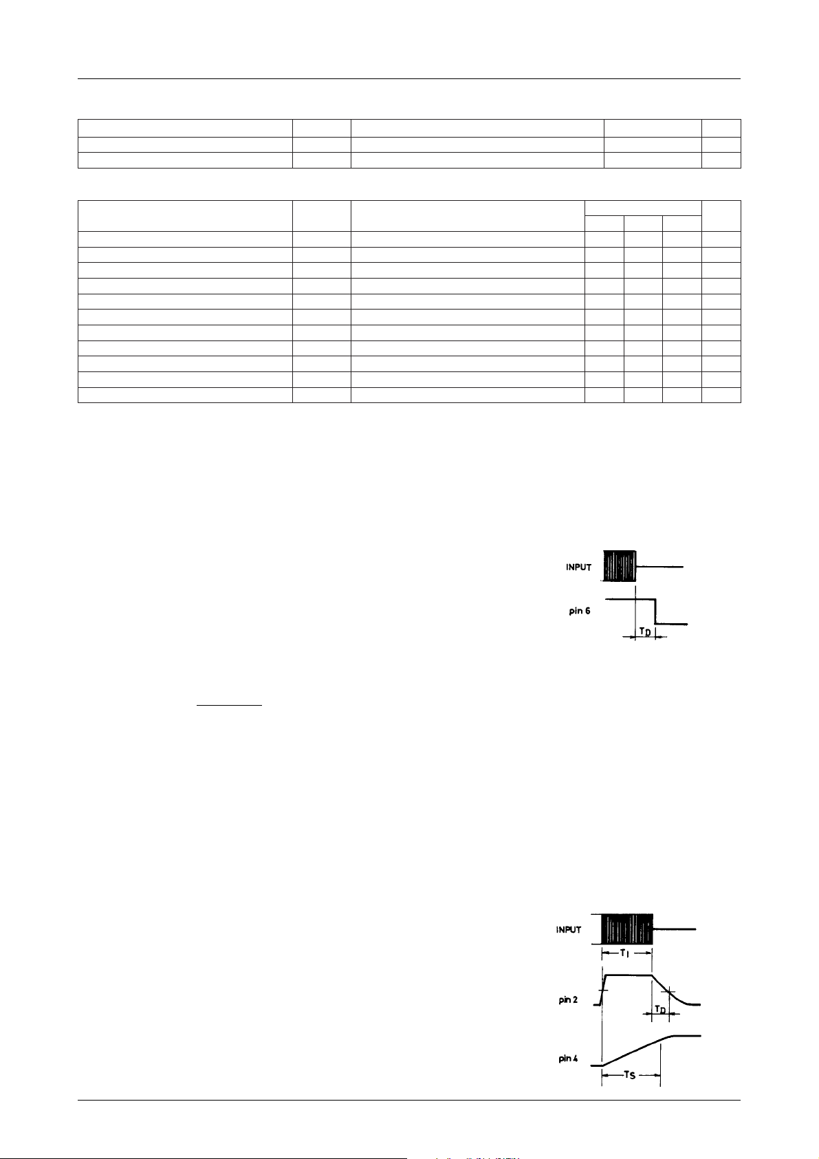
Description of Operatin (See Timing Chart.)
When power is applied, the reset circuit operates to initialize the circuit. The reset time depends on the capacitance
value of C5 on pin 8 and no input signal is accepted while the reset circuit is operating. When the reset mode is
released and the input signal exceeds the input check level, C, R on pin 2 are charged and the pontential on pin 2
rises, thereby causing the comparator (1) to be inverted. When the comparator (1) is inverted, pin 4 (C4) is charged
and the potential on pin 4 begins rising. When this potential exceeds the threshold voltage, the comparator (2) is
inverted and the program presence mode is memorized ; thus the potential on pin 4 is held at High level. During
this period of time, the output (pin 6) is held at High level. When the signal disappears and the comparator (1) is
inverted, the output (pin 6) turns to Low level, thereby causing the plunger to be driven.
The reset pulse is generated for a certain period of time each time power is applied, thereby causing the circuit to
be initialized.
Timing Chart
Proper Cares in Using IC
· Maximum Ratings
If the maximum ratings are exceeded, breakdown or deteroration may result. Use the IC in the range where the
maximum ratings are not exceeded.
· Pin-to-pin Short and Inverted Insertion
These may cause breakdown or deterioration to occur. Be extremely careful when mounting the IC on the board.
· The voltage on pin 1 must not exceed that on pin 9.
· The current flowing into pin 2 and pin 4 must not exceed ±0.5mA continuously.
· The voltage on pin 8 is 2.5V max. and must not exceed that on pin 7.
· Electrolytic capacitors are used to set the recorded area detect time and reset time. The actual time constants are
15 to 20% larger than the calculated values obtained by using the catalon values of such capacitors. For polyester
film capacitor and tantalum electrolytic capacitor, the calculated values hold to a fairly good approximation.
No.1343–3/8
Page 4

Test Circuit
LA2010
metItseTlobmySWSyratoR1-WS2-WSsnoitidnoC
levelkcehctupnIV
levelNO)1(rotarapmoCV
levelFFO)1(rotarapmoCV
levelNO)2(rotarapmoCV
levelFFO)2(rotarapmoCV
1egatlovteser8niPV
2egatlovteser8niPV
levelteser4niPV
tnerructiucriCI
rotsisnarttuptuO
egatlovnoitarutas
edoidtuptuO
egatlovnoitarutas
NI
H-1HT
L-1HT
H-2HT
L-2HT
1-R8
2-R8
R4
CC
V
EC
V
F
111
211
211
311
311
412
512
512 Vegatlov4niperusaeM
511 .tnerrucylppuserusaeM
)tas(611 Vegatlov6niperusaeM
621 Vegatlov6niperusaeM
L6nipta → noisrevniH
H6nipta → noisrevniL
H6nipta → noisrevniL
L6nipta → noisrevniH
Vta
L6niptaVVleveltupniCAerusaeM →H
noisrevni1niptaegatlov
noisrevni4niptaegatlov
.V1=
1
.Am006ta
.Am006ta
.edomnoisrevni
V2niperusaeM
.edom
.edom
.edom
.edom
.edom
.edom
4
V2niperusaeM
4
V4niperusaeM
2
V4niperusaeM
2
VerusaeM
1
VerusaeM
1
2
3
3
No.1343–4/8
Page 5

Equivalent Circuit Block Diagram
Sample Application Circuit
LA2010
No.1343–5/8
Page 6

LA2010
No.1343–6/8
Page 7

LA2010
No.1343–7/8
Page 8

LA2010
Specifications of any and all SANYO products described or contained herein stipulate the performance,
characteristics, and functions of the described products in the independent state, and are not guarantees
of the performance, characteristics, and functions of the described products as mounted in the customer's
products or equipment. To verify symptoms and states that cannot be evaluated in an independent device,
the customer should always evaluate and test devices mounted in the customer's products or equipment.
SANYO Electric Co., Ltd. strives to supply high-quality high-reliability products. However, any and all
semiconductor products fail with some probability. It is possible that these probabilistic failures could
give rise to accidents or events that could endanger human lives, that could give rise to smoke or fire,
or that could cause damage to other property. When designing equipment, adopt safety measures so
that these kinds of accidents or events cannot occur. Such measures include but are not limited to protective
circuits and error prevention circuits for safe design, redundant design, and structural design.
In the event that any or all SANYO products(including technical data,services) described or
contained herein are controlled under any of applicable local export control laws and regulations,
such products must not be exported without obtaining the export license from the authorities
concerned in accordance with the above law.
No part of this publication may be reproduced or transmitted in any form or by any means, electronic or
mechanical, including photocopying and recording, or any information storage or retrieval system,
or otherwise, without the prior written permission of SANYO Electric Co. , Ltd.
Any and all information described or contained herein are subject to change without notice due to
product/technology improvement, etc. When designing equipment, refer to the "Delivery Specification"
for the SANYO product that you intend to use.
Information (including circuit diagrams and circuit parameters) herein is for example only ; it is not
guaranteed for volume production. SANYO believes information herein is accurate and reliable, but
no guarantees are made or implied regarding its use or any infringements of intellectual property rights
or other rights of third parties.
This catalog provides information as of January, 2000. Specifications and information herein are subject
to change without notice.
PS No.1343–8/8
 Loading...