

SANYO LA1867NM Datasheet
Ordering number : EN4619B
32096HA (OT)/D2593TS (OT) No. 4619-1/32
Overview
The LA1867M is a high-performance multifunction (FMIF, noise canceller, MPX and MRC) single-chip tuner IC
for use in car radios. High-quality tuners with superlative
cost-performance characteristics can be constructed easily
using this IC.
Functions
• FM-IF
• Noise canceller
• MPX
• MRC (multipath noise reduction circuit)
Features
• Forms a high-performance FM tuner when combined
with the Sanyo LA1193 FM front-end IC.
• Multiple functions, MRC circuit, dual diversity, and
RDS handling
• High performance, high sensitivity and high stability
(excellent temperature characteristics)
• High audio quality and noise reduction according to the
reception conditions.
• Miniaturization of the required external capacitors
(electrolytic capacitors no longer required)
• Easy adjustment (The SD, muting and SNC circuits are
separated.)
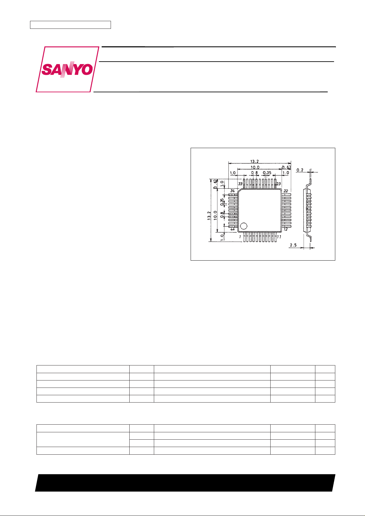
Package Dimensions
unit: mm
3148-QIP44MA
SANYO: QIP44MA
[LA1867NM]
LA1867NM
SANYO Electric Co.,Ltd. Semiconductor Bussiness Headquarters
TOKYO OFFICE Tokyo Bldg., 1-10, 1 Chome, Ueno, Taito-ku, TOKYO, 110-8534 JAPAN
Car Radio Single-Chip Tuner System
Monolithic linear IC
Specifications
Maximum Ratings at Ta = 25°C
Operating Conditions at Ta = 25°C
Parameter Symbol Conditions Rating Unit
Maximum supply voltage V
CC
max Pins 4 and 31 9.2 V
Allowable power dissipation Pdmax 740 mV
Operating temperature Topr –40 to +85 °C
Storage temperature Tstg –40 to +150 °C
Parameter Symbol Conditions Rating Unit
Recommended supply voltage
V
CC
Pins 4 and 31 8.0 V
V
CC ST/SD
Pins 29 and 44 5.0 V
Operating supply voltage range V
CC
op 7.0 to 9.0 V
Operating Characteristics at Ta = 25°C, VCC= 8.5 V (Note that these measurements are made using
the IC-51-044-464 IC socket manufactured by Yamaichi Electric Works, Ltd.)
Note: * Unless otherwise specified, with an IHF-BPF/T200 inserted in the pin 7 and 8 MPX output circuit.
No. 4619-2/32
LA1867NM
Parameter Symbol Conditions
Rating
Unit
min typ max
[FM BLOCK]
Quiescent current I
CCO-FM
No input (I4+ I31) 40 55 70 mA
Demodulator output V
O-FM
10.7 MHz, 100 dBµ, 1 kHz,
175 260 350 mVrms
100% mod, pin 7 output
Channel balance C
B
10.7 MHz,100 dBµ, 1 kHz, 100% mod, the
–1.0 0 +1.0 dB
ratio of pin 7 to pin 8, Referenced to pin 7.
Total harmonic distortion THD-
FMmono
10.7 MHz, 100 dBµ, 1 kHz,
0.2 1.0 %
100% mod, pin 7
Signal-to-noise ratio (IF) S/N-
FM
IF
10.7 MHz,100 dBµ, 1 kHz,
73 80 dB
100% mod, pin 7
AM suppression ration (IF) AMRIF
10.7 MHz,100 dBµ 1 kHz, fm = 1 kHz,
57 70 dB
Pin 7 when the AM modulation is 30%
Att-1
10.7 MHz, 100 dBµ, 1 k Hz, the pin 7
20 25 30 dB
attenuation when V
22
goes from 0 to 1 V
Muting attenuation
Att-2
10.7 MHz, 100 dBµ, 1 k Hz, the pin 7
28 33 38 dB
attenuation when V
22
goes from 0 to 2 V
Channel separation Separation
10.7 MHz, 100 dBµ, L + R = 90%,
30 40 dB
pilot = 10%, the pin 7 output ratio
Stereo on level ST-
ON
The pilot modulation level such that V
44
1.5 2.9 5.0 %
becomes less than 0.5 V*
Stereo off level ST-
OFF
The pilot modulation level such that V
44
0.8 1.9 %
becomes greater than 3.5 V*
Total harmonic distortion THD-
MainL
10.7 MHz, 100 dBµ, L + R = 90%,
0.3 1.0 %
pilot = 10%, pin 7
10.7 MHz, 100 dBµ, pilot = 10%
,
Pilot cancellation P
CAN
pin 7 signal/PILOT-LEVEL leakage, 20 35 dB
DIN-audio filter
SNC output voltage V
OSUB
10.7 MHz, 100 dBµ, L – R = 90%,
3 10 mVrms
pilot = 10%, V
13
= 0.1 V, pin 7
SNC output attenuation Att
SNC
10.7 MHz, 100 dBµ, L – R = 90%,
2 6 10 dB
pilot = 10%, V
13
= 3 V to 0.6 V, pin 7
Att
HCC-1
10.7 MHz, 100 dBµ, 10 kHz, L + R = 90 %,
2 6 10 dB
pilot = 10%, V
14
= 3 V to 0.6 V, pin 7
HCC output attenuation
Att
HCC-2
10.7 MHz,100 dBµ, 10 kHz, L + R = 90 %,
6 10 14 dB
pilot = 10%, V
14
= 3 V to 0.1 V, pin 7
10.7 MHz, 100dBµ, 100% mod, IF input
Input limiting voltage Vi-lim
such that the input reference output is
33 42 51 dBµ
down by –3 dB, when the soft muting
function is operating
Muting sensitivity Vi-Mute
The IF unmodulated input level when
32 40 48 dBµ
V
23
is 2 V.
SD sensitivity SD
sen
The unmodulated IF input such that the SD
64 74 84 dBµ
pin voltage (V29) becomes 3.5 V or higher.
IF counter buffer output V
IFBUFF-FM
10.7 MHz, 100 dBµ, unmodulated,
160 230 320 mVrms
the pin 19 output
AM output V
O-AM
The pin 7 output in AM mode (AC2=
234 330 466 mVrms
300 mV rms, 1 kHz, the pin 20 input)
Continued on next page.
Continued from preceding page.
Block Functions
1. FM-IF
• IF-limiter amplifier
• S-meter outputs (three systems)
• Quadrature detector
• AF preamplifier
• AFC output
• Muting circuit (band mute, weak input mute, soft mute)
• Control pins (SD, muting attenuation, soft mute on level)
• SD output
• IF counter buffer output
• S-meter output shifter
2. Noise canceller
• Built-in high-pass filter
• Built-in low-pass filter delay circuit
• Noise AGC
• Pilot signal compensation circuit
• Noise reduction setting pin
• Noise canceller off in AM mode function
• High-pass filter “fc” control pin
No. 4619-3/32
LA1867NM
Parameter Symbol Conditions
Rating
Unit
min typ max
[FM BLOCK]
V
SMFM-1
No input, pin 32 DC output,
0.0 0.1 0.3 V
non-mod, SW-2 open
V
SMFM-2
50 dBµ, pin 32 DC output,
1.0 2.1 3.3 V
Signal meter output
non-mod, SW-2 open
V
SMFM-3
70 dBµ, pin 32 DC output,
2.3 3.5 5.3 V
non-mod, SW-2 open
V
SMFM-4
100 dBµ, pin 32 DC output,
4.7 6.0 6.7 V
non-mod, SW-2 open
Muting bandwidth BW-Mute
100 dBµ, The bandwidth when V
23
= 2 V,
110 190 290 kHz
non-mod
Muting drive output V
Mute-100
100 dBµ, pin 23 DC output, non-mod 0.00 0.03 0.20 V
[N.C BLOCK] Noise Canceller Input (pin 20), PG1
f = 1 kHz, 1 µs, with a 100 mV p-o pulse
t
GATE
1 input, the time for V40to become 1 V 35 55 75 µs
or higher
Gate time
f = 1 kHz, 1 µs, with a 100 mV p-o pulse
t
GATE
2 input, with the MRC pin 15 input = 1 kHz, 10 25 40 µs
30 mV rms
With a 1 kHz signal such that the noise
Noise sensitivity S
N
canceller operation is on, the 1 µs pulse 50 75 mVp-o
input level, measure pin 20.
[Multipath suppression circuit] MRC Input (AC1)
MRC output V
MRC
V18= 2 V, 1 kHz, 5 mV rms, the pin
1.75 1.85 1.95 V
12 voltage when there is a pin 15 input
MRC operating level MRC-ON
V
18
= 2 V, the pin 15 input level such
15 30 mVrms
that V12 becomes 1.75 V

3. MPX
• Nonadjusting VCO (912 kHz)
• Level-following type pilot cancelation circuit
• SNC
• FM HCC
• Stereo/mono display output
• Built-in anti-birdie stereo decoder
• Automatic stereo/mono switching
4. MRC
• DC level shifter circuit
• Noise amplifier
• Noise detection circuit
• Time constant control circuit
Block Features
1. FM-IF
• The development of a high performance S-meter circuit has simplified all types of control.
— High linearity S-meter circuit (6-stage detection type)
— High quality S-meter (superlative temperature characteristics)
• High quality design
— Design that emphasizes temperature characteristics
— S-meter, SD sensitivity, –3 dB L.S., etc.
• Improved active characteristics
— Muting circuit time constant control (Since the attack and recovery time can be set independently, the audio
quality under multipath conditions can be improved.)
— Three built-in S-meter circuits
Soft mute/HCCtime constants
SD time constants Application design is eased since these can all be set independently.
SNC time constants
2. Noise canceller
• Noise canceller error prevention when a narrow band (150 kHz) ceramic filter is used
• A new noise canceller system was developed.
— Reduced noise canceller errors during overmodulated signal reception.
— Reduced noise canceller errors under continuous noise conditions.
• Miniaturization of the required external capacitors
No. 4619-4/32
LA1867NM

3. MPX
• Miniaturization of the required external components (nonadjusting 912 kHz VCO)
• Improved basic performance
— Pilot cancelation level (30 dB typ.)
— No variation in mono output level due to separation adjustment (subcarrier output level adjustment type
separation adjustment)
— A new SNC curve was developed.
— Built-in anti-birdie filters (114 kHz and 190 kHz)
— Improved high region separation characteristics
— Improved stereo signal-to-noise ratio
4. MRC
• Controls the SNC and HCC circuit control signals by detecting the field strength (S-meter) and multipath noise.
No. 4619-5/32
LA1867NM
Test Circuit
No. 4619-6/32
LA1867NM
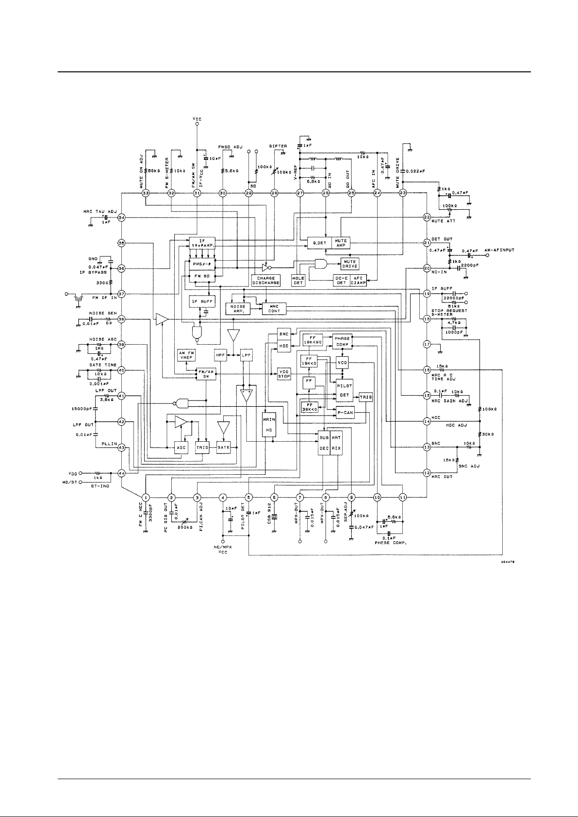
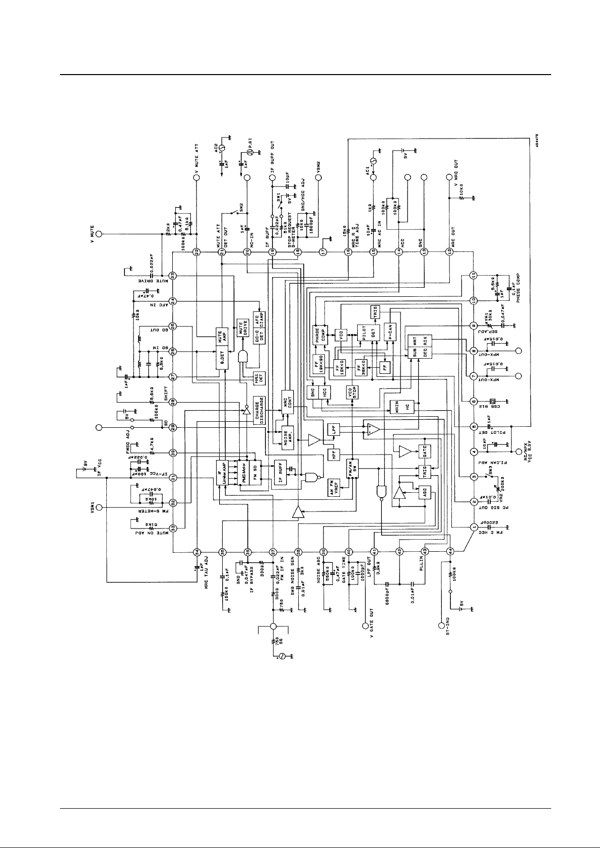
Block Diagram and Peripheral Circuits
No. 4619-7/32
LA1867NM
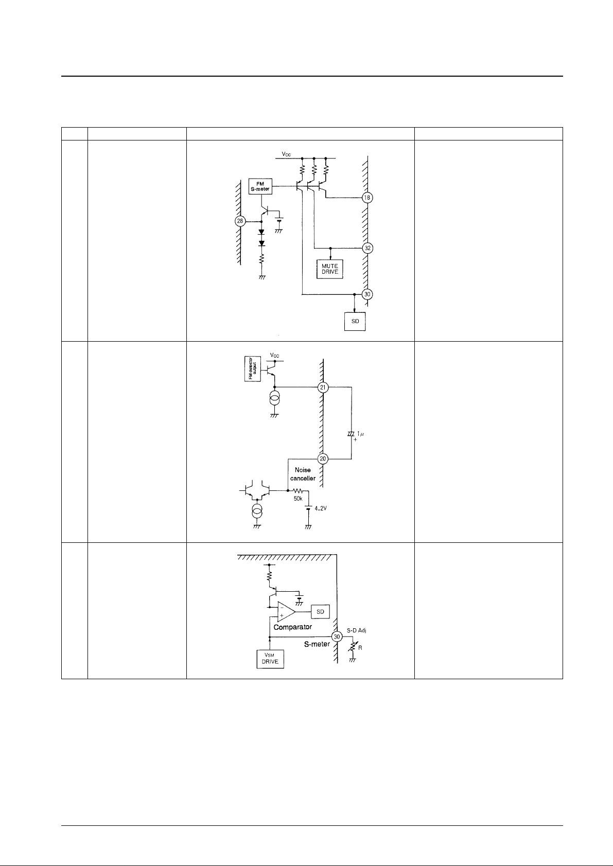
Pin Functions
FM-IF Block
No. 4619-8/32
LA1867NM
Continued on next page.
Pin Function Equivalent internal circuit Note
18
S-meter output for MRC
and SNC
32
S-meter output for muting
drive and HCC
30 S-meter output for SD
28
S-meter output shift control
pin
20 Noise canceller input
21 FM detector output
30 FM SD Adj
Constant current drive type
The slope can be changed by changing the
value of the S-meter output resistance.
The field strength can be shifted in the
positive or negative direction with an
external resistor on pin 28 without changing
the S-meter slope.
Noise canceller input
The input impedance is 50 kΩ.
FM detector output
Low impedance in FM mode
Pin 30
The comparison voltage is determined by
the external resistor.
Pin 30 is the S-meter output, and SD turns
on when it exceeds the internal supply
voltage.
Unit (resistance:Ω, capacitance:F)
Continued from preceding page.
No. 4619-9/32
LA1867NM
Continued on next page.
Pin Function Equivalent internal circuit Note
37 FM IF IN
36 IF BYPASS
23 Mute drive output
22 Mute input
33 FM mute ON Adj
Limited amplifier input
Select the capacitor grounding point
carefully.
➀ The muting time constants from the
external CR circuit are determined as
follows.
Attack time T
A
= R1× C
2
Release time TR= R2× C
2
➁ Noise convergence adjustment
Divide the V
23
voltage by R2when
there is no input at the antenna input,
and input that voltage to pin 22.
Noise convergence will be maximum
when V
22
= 2 V.
The variation range is 5 to 35 dB,
taking the 1 kHz 22.5 kHz dev output
as the reference.
➂ Muting off function
The muting is turned off when pin 22 is
shorted to ground.
The muting on level is adjusted by changing
the external resistance R.
Unit (resistance:Ω, capacitance:F)
Continued from preceding page.
No. 4619-10/32
LA1867NM
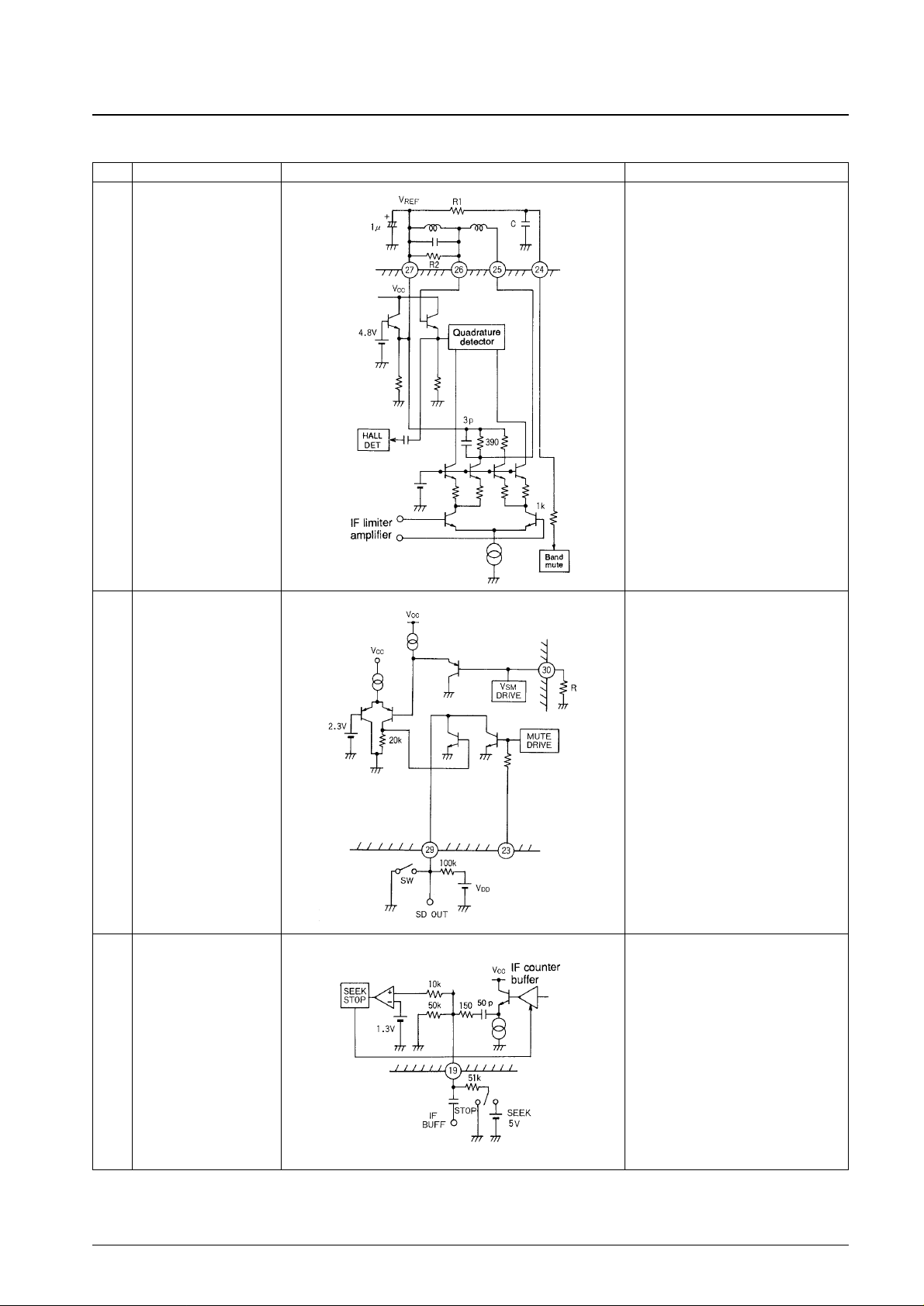
Pin Function Equivalent internal circuit Note
24 AFC
25 QD OUT
26 QD IN
27 V
REF
29 SD pin
30
SD sensitivity adjustment
pin
19
IF counter buffer
Seek/stop switch
• R
1
is the resistor that determines the band
muting bandwidth.
Increasing R
1
reduces the bandwidth.
Decreasing R
1
increases the bandwidth.
• Null voltage
When tuned, the voltage between pins 24
and 27 will be 0 V.
V24– V27= 0 V
The band muting is turned on when
| V24– V
27
| ≥ 0.7 V.
The SD output for the pin 30 SD.
R determines the SD sensitivity.
Pin 23 is coupled to the muting drive output.
SD operates when the switch is off.
This pin is used for both the IF counter
buffer (AC output) and the seek/stop switch
(DC input).
It is not coupled to the SD output.
The IF buffer is turned on and off by the pin
19 DC bias level.
Pin 19: high → buffer on, low → buffer off.
Unit (resistance:Ω, capacitance:F)
 Loading...