

SANYO LA1862M Datasheet
Ordering number: EN 4092B
Monolithic Linear IC
LA1862M
Single-chip Tuner System for Car Stereo
Overview
The LA1862M is a single-chip car stereo FM IF/NC/MPX
tuner IC which offers improved IF stability and S-meter
characteristics, compared with the LA1861M.
The LA1862M makes the design of high-performance FM
tuners at low cost easy.
Functions
.
IF amplifier
.
Peak detector
.
AF preamplifier
.
AFC output
.
S-meter driver
.
Soft mute circuit
.
IF buffer output
.
Noise canceller
.
Adjustment-free VCO
.
Pilot signal canceller
.
SNC High-cut control (HCC)
Features
.
Pin compatible with the LA1861M
.
Improved I/O S-meter characteristics
.
Excellent sound quality at low input levels
.
Easy adjustment of muting characteristics
.
Because this device has a 36-pin flat package, it requires few
external components and offers excellent cost performance.
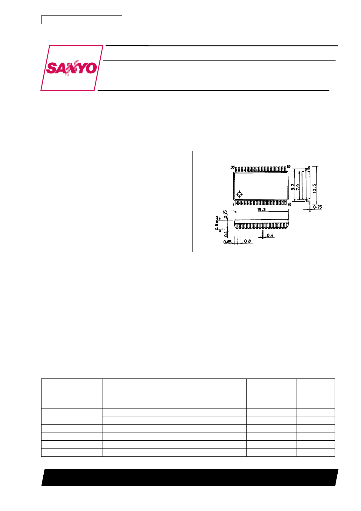
Package Dimensions
unit : mm
3129-MFP36S
[LA1862M]
SANYO : MFP36S
Specifications
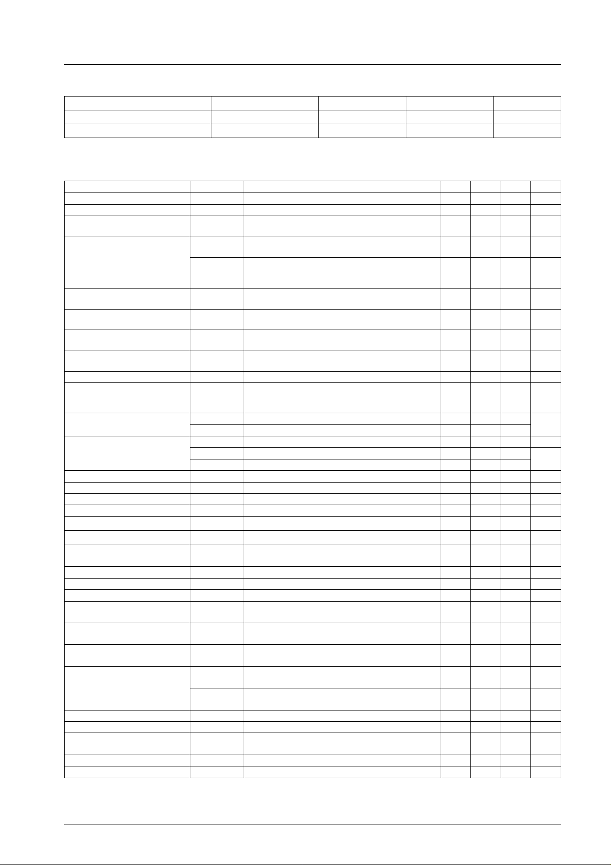
Maximum Ratings at Ta = 25°C
Parameter Symbol Conditions Ratings Unit
Maximum supply voltage V
Allowable power
dissipation
Input voltage V
Input current I
Output current I
Operating temperature Topr –30 to +80 °C
Storage temperature Tstg –40 to +150 °C
max Pin 8 10 V
CC
Pd max Ta = 25°C 720 mW
IF Pin 36-35 (IF input) ±0.7 Vp-p
IN
V
MPX Pin 26 (NC-MPX input) 1.0 Vrms
IN
max Pin 25 (stereo lamp drive current) 20 mA
L
max Pin 5 (SD output) 1.0 mA
SD
SANYO Electric Co.,Ltd. Semiconductor Bussiness Headquarters
TOKYO OFFICE Tokyo Bldg., 1-10, 1 Chome, Ueno, Taito-ku, TOKYO, 110-8534 JAPAN
63098HA(II)/N0893TS A8-8753/O022 TS No.4092-1/27
LA1862M
Operating Conditions at Ta = 25°C
Parameter Symbol Conditions Ratings Unit
Recommended supply voltage V
Operating supply voltage range V
CC
op 7.5 to 10 V
CC
Operating Characteristics at Ta = 25°C, VCC= 8.5 V, f = 10.7 MHz, unless otherwise noted SW-1
is off.
Parameter Symbol Conditions min typ max Unit
Quiescent current I
Current drain I
CCO
CC-100
Demodulator output voltage V
THD 1
Total harmonic distortion
THD 2
Signal-to-noise ratio S/N
Input limiting voltage V
IN lim
Muting attenuation (1) Mute
Muting attenuation (2) Mute
Muting bandwidth BW
AM rejection ratio AMR
V
Muting drive output voltage
S-meter output voltage
V
5-100
V
V
V
1-100
5-0
1-0
1-50
IF COUNT output sensitivity IF input level at IF COUNT ON. SW-1 is ON. 44 53 62 dBµ
IF buffer output voltage V
IF-ON
Input impedance Z
Output noise voltage V
Gate time t
NO
gate VIN
Noise sensitivity SN V
Channel separation Sep
Stereo indicator threshold level Pilot signal level when the LED turns ON. 1.0 2.5 5.0 %
Stereo indicator hysteresis hy LED ON level - LED OFF level 3.2 6.5 dB
Capture range C.R CR = | (f – 456)/456 x 100 |±1.2 %
SCA rejection ratio SCA rej
SNC output attenuation Att
SNC output voltage V
Att
SNC
Osub
HCC
High-out control attenuation
Att
HCC
Ripple rejection R
Channel balance CB | Pin 15 output – pin 16 output | 0 1.5 dB
Pilot signal attenuation
Stereo indicator LED current Minimum stereo drive current 1.0 mA
Pin 25 saturation voltage I
Note: When a filter is not specified, connect an IHF bandpass filter to the MPX outputs.
No input signal 45 70 mA
VIN= 100 dBµ 47 72 mA
VIN=100dBµ,f=1kHz,
O
100% modulation, pin 15 output
Mono, V
100% modulation, pin 15 output
=100dBµ,f=1kHz,
IN
Stereo (L + R),
V
=100dBµ,f=1kHz,
IN
100% modulation, pin 15 output
V
=100dBµ,f=1kHz,
IN
100% modulation
VIN= 100 dBµ reference, 3 dB audio output
attenuation, IF input level, soft muting ON
V5=5V,VIN=100dBµ,f=1kHz,
Att
100% modulation
V5=2V,VIN=100dBµ,f=1kHz,
Att
100% modulation
MuteVIN
= 100 dBµ, V5 = 2 V 135 200 305 kHz
V
= 100 dBµ, 400 Hz, 100% modulated FM
IN
carrier. 1 kHz, 30% modulated AM interference
signal
No input signal 3.5 4.7
VIN= 100 dBµ 0 0.3
No input signal 0.1 0.5 V
VIN= 50 dBµ 1.1 1.9 2.7
VIN= 100 dBµ 5.4 6.4 7.4
VIN= 100 dBµ. SW-1 is ON. 200 300 480 mVrms
f = 1 kHz 20 kΩ
in
Pin 26 connected to ground 27 µV
= 100 mVp-p, 1 µs pulsewidth,f=1kHz
= 1 µs pulsewidth,f=1kHz 35 mVp-o
IN
f = 1 kHz, 90% L+R signal modulation. 10% pilot
signal modulation, IHF bandpass filter.
90% L + R signal modulation. 10% pilot signal
modulation. 67 kHz, 10% modulated SCA signal
V14 = 0.6 V, 90% L – R signal modulation. 10%
pilot signal modulation
V14 = 0.1 V, 90% L – R signal modulation. 10%
pilot signal modulation
V13 = 0.6 V, 90% L + R signal modulation. 10%
1
pilot signal modulation
V = 1.1 V, 90% L + R signal modulation. 10% pilot
2
signal modulation
f = 50 Hz, V = 100 mVrms 27 dB
r
Left channel adjusted and measured
DIN audio filter. See Note.
=10mA 1.0 V
L
8.5 V
225 350 495 mVrms
0.3 1.2 %
0.3 1.2 %
64 71 dB
32 41 50 dBµ
21 25 29 dB
510 15dB
47 60 dB
13 23 35 µs
36 50 dB
75 dB
–12.0 –7.5 –3.0 dB
5mV
–15 –5 0 dB
–2.0 0 dB
15 22 dB
V
V
No. 4092- 2/27
LA1862M
Specified board (80 × 40 × 2mm3glass epoxy resin)
Independent IC
Test Circuit
Allowable power dissipation, Pd max – mW
Ambient temperature, Ta – °C
Unit (resistance: Ω, capacitance: F)
No. 4092- 3/27
LA1862M
Pin Description
Pin No. Description
1 S-meter output
2 IF buffer sensitivity control
3 IF buffer output
4 Muting threshold control
5 Muting drive control output
6 Noise sensitivity control
7 Noise AGC sensitivity control
8 Supply voltage (V
9 Gate time control output
10 Peak hold network connection
11 Lowpass filter output
12 High-cut attenuation control
13 High-cut control input
14 SNC control input
15 MPX left-channel audio output
16 MPX right-channel audio output
17 Pilot cancel signal input
18 Pilot cancel signal output
19 Pilot detector capacitor connection 1
20 Pilot detector capacitor connection 2
21 External VCO (F23) connection
22 Phase detector network connection 1
23 Phase detector network connection 2
24 PLL input
25 Stereo indicator LED driver output
26 Noise canceller input
27 Ground
28 Audio muting amplifier output (AF output)
29 AFC output
30 Peak detector input
31 IF signal output
32 Muting attenuation control
33 Voltage reference output
34 Pilot signal canceller detector
35 IF input
36 IF bypass input
CC
)
No. 4092- 4/27
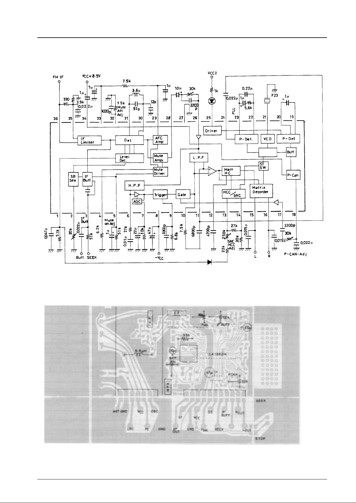
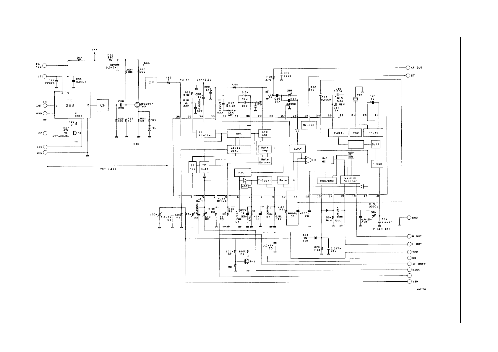
Sample Application Circuit
LA1862M
Frequency
divider
PCB Pattern
Unit (resistance: Ω, capacitance: F)
Unit (resistance: Ω, capacitance: F)
No. 4092- 5/27
(Mitsumi)
Sample Application Circuit (USA)
No. 4092- 6/27
gain
Note 1: Used to change the SD sensitivity
Note 2: When LOC goes HIGH, the IF count and SD
sensitivity shift by 25 dB
Frequency
divider
Unit (resistance: Ω, capacitance: F)
LA1862M
See note 1.
LA1862M
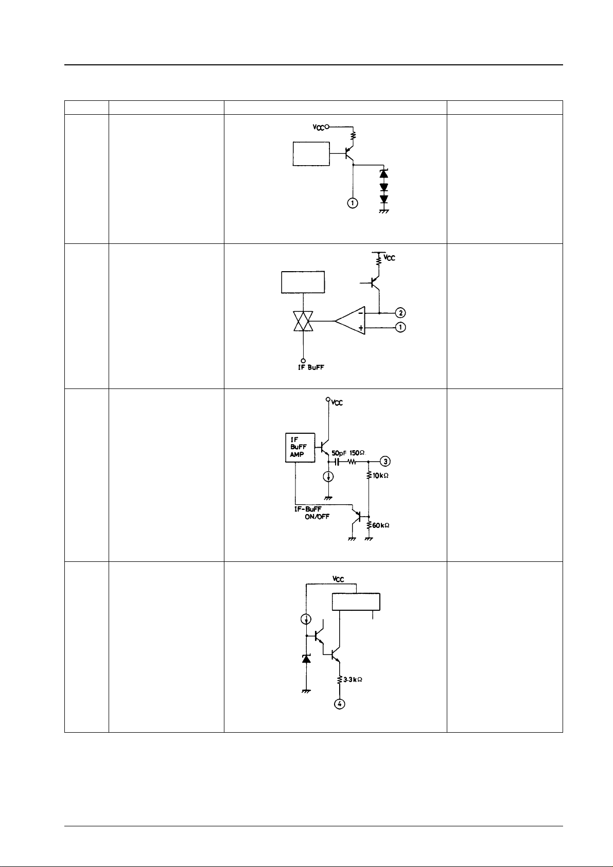
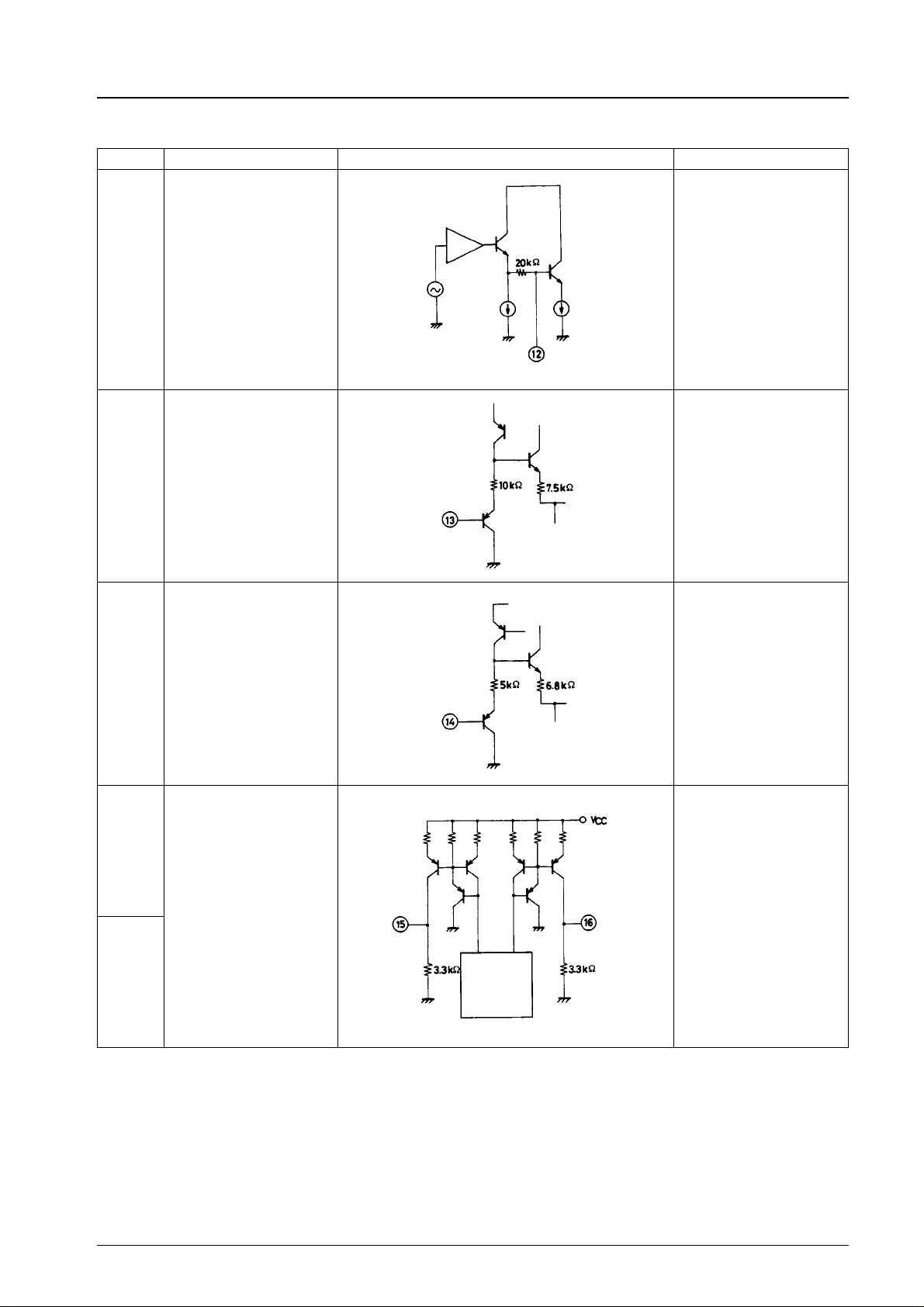
Pin Functions
Pin No. Function Equivalent circuit Remarks
FM
S-meter
detector
1 S-meter output
IF amplifier
2 IF buffer ON adjust
Current-drive waveform
S-meter circuit
3 IF buffer output
4 Mute adjust
Inversion circuit
Control signal:
SEEK when HIGH (V
STOP when LOW (GND)
Pin 3 should be left open if
not using the IF count
DD
Continued on next page.
)
No. 4092- 7/27
LA1862M
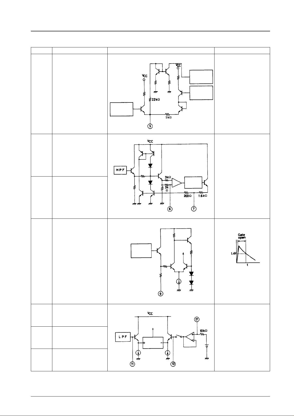
Continued from preceding page.
Pin No. Function Equivalent circuit Remarks
Mute
circuit
5 Mute drive
6 Noise sensitivity adjust
7 NoiseAGC
S-meter
detector
Mute band
detector
Noise
demodulator
9 Gate time adjust
10 Memory circuit
11 LPF output
17 Pilot cancel signal input
Pulse
detector
To MPX
input
Subtraction
circuit
Gate
Gate
circuit
Pin 9
voltage
The gate is open when the
voltage on pin 9 is 1.4 V
(2V
) or higher.
D
Continued on next page.
No. 4092- 8/27
LA1862M
Continued from preceding page.
Pin No. Function Equivalent circuit Remarks
Composite signal
12 High-cut capacitive coupling
13 HCC control input
14 SNC control input
High-cut frequency set pin
15
16
MPX outputs
Output R = 3.3 kΩ
Load R built-in
Multiplier
Continued on next page.
No. 4092- 9/27
 Loading...