

SANYO LA1837 Datasheet
Overview
The LA1837 is a single-chip AM/FM IF and MPX IC that
supports electronic tuning and was developed for use in
home stereo systems. It is optimal for use in automatic
station selection systems that use the SD and IF counting
techniques.
Functions
AM: RF amplifier, mixer, oscillator, IF amplifier,
detector AGC, oscillator buffer, S-meter, narrowband SD, IF buffer
FM IF: IF amplifier, quadrature detector, S-meter, S-
curve detector, IF buffer output
MPX: PLL stereo decoder, stereo display, forced mono,
VCO stop, post amplifier, audio muting, adjacent
channel interference rejection function
Features
• On-chip MPX VCO (no external components required)
• Adjacent channel interference rejection function
(third and fifth order)
• Supports both the SD and the IF counting techniques.
•
The AM and FM SD sensitivities can be set independently.
•
The AM and FM output levels can be set independently.
•
Improved AM practical sensitivity and high-input
distortion characteristics
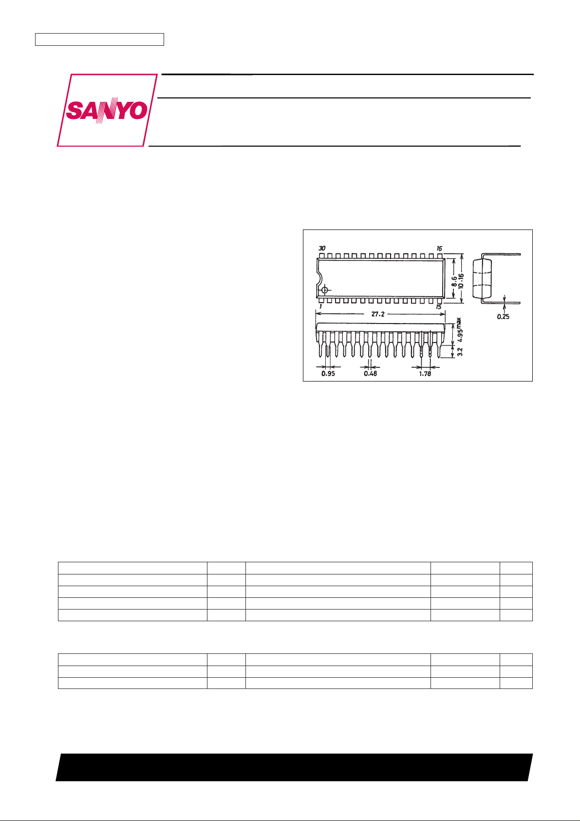
Package Dimensions
unit: mm
3061-DIP30S
Monolithic Linear IC
Ordering number : EN5688
82097HA(OT) No. 5688-1/9
SANYO: DIP30S
[LA1837]
SANYO Electric Co.,Ltd. Semiconductor Bussiness Headquarters
TOKYO OFFICE Tokyo Bldg., 1-10, 1 Chome, Ueno, Taito-ku, TOKYO, 110 JAPAN
Single-Chip Home Stereo IC with
Electronic Tuning Support
LA1837
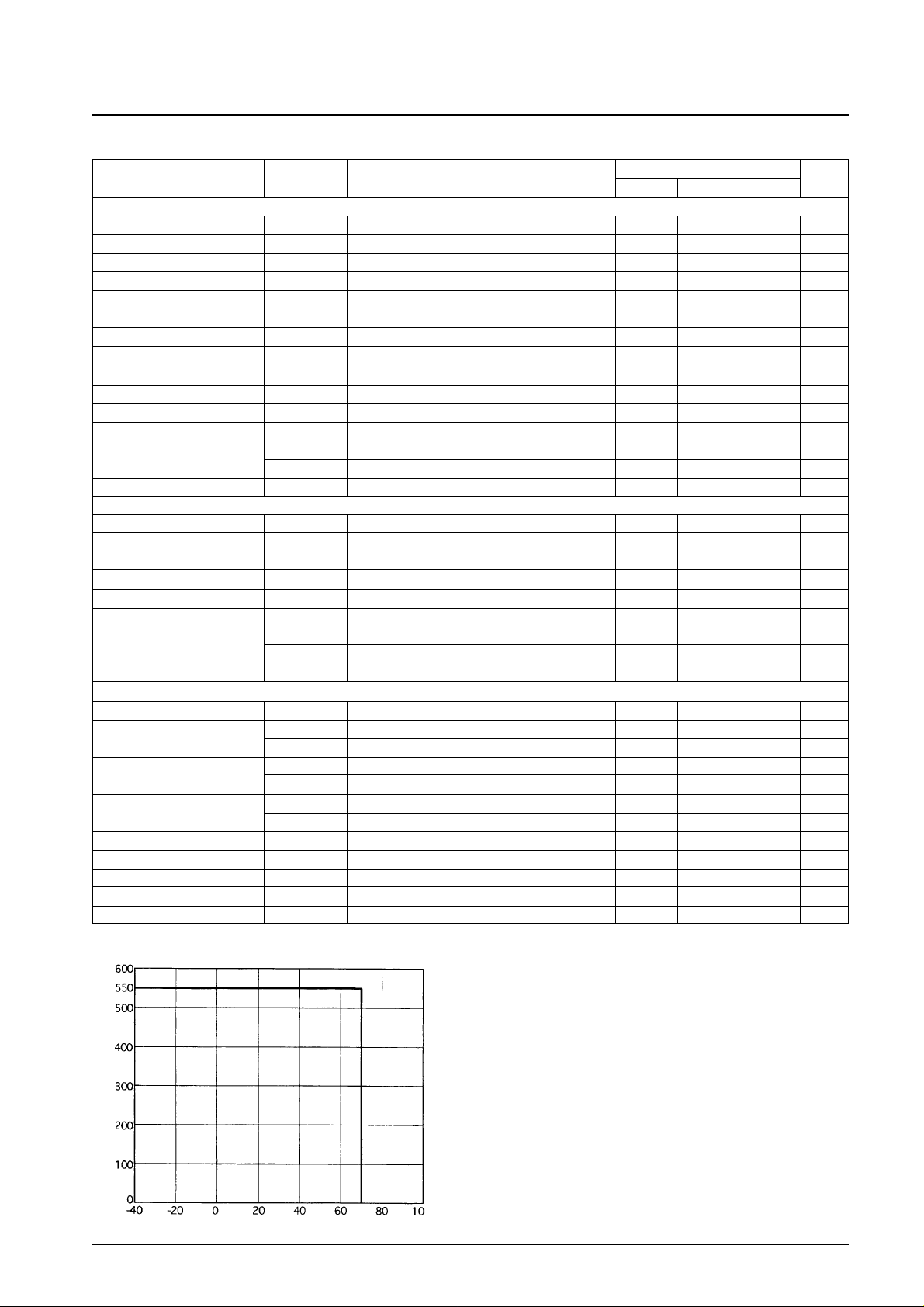
Parameter Symbol Conditions Ratings Unit
Maximum supply voltage V
CC
max 12 V
Allowable power dissipation Pd max Ta ≤ 70°C 550 mW
Operating temperature Topr –20 to + 70 °C
Storage temperature Tstg –40 to +125 °C
Specifications
Maximum Ratings at Ta = 25°C
Parameter Symbol Conditions Ratings Unit
Recommended supply voltage V
CC
9V
Operating voltage range V
CC
op 7 to 11 V
Operating Conditions at Ta = 25°C
No. 5688-2/9
LA1837
Parameter Symbol Conditions
Ratings
Unit
min typ max
[FM Mono Characteristics] fc = 10.7 MHz, fm = 1 kHz, with the coil adjusted so that V
AFC
– V
REG
= 0 V
Current drain I
CCO
-FM
With no input 18 31 44 mA
Demodulation output V
O
FM
100 dBµ, 100% mod. The pin 16 output 730 1100 1460 mVrms
Channel balance C.B-mono 100 dBµ, 100% mod. The pin 16 output/pin 17 output –1.5 0 +1.5 dB
Total harmonic distortion (mono) THD
FM(1)
100 dBµ, 100% mod. The pin 16 output 0.3 1.3 %
Total harmonic distortion (mono) THD
FM(2)
100 dBµ, 200% mod. The pin 16 output 1.0 5 %
Signal-to-noise ratio S/N
FM
100 dBµ, 100% mod. The pin 16 output 72 80 dB
AM rejection ratio AMR 100 dBµ, AM 30 % mod. The pin 16 output 45 65 dB
Limiting input voltage –3 dBL.S.
100 dBµ, 100% mod. Referenced to the output.
26 32 38 dBµ
The input such that the output is down –3 dB.
LED sensitivity SD
On-FM
51 60 69 dBµ
LED bandwidth SD
BW
100 dBµ 85 120 170 kHz
IF count buffer output V
IFBuff-FM
100 dBµ. The pin 13 output 80 120 160 mVrms
S-meter output
V
SM-FM(1)
0 dBµ. The pin 11 output 0 0.1 0.5 V
V
SM-FM(2)
100 dBµ. The pin 11 output 3.6 4.3 5.0 V
Muting attenuation Mute-Att 100 dBµ, 100% mod. The pin 16 output 75 85 dB
[FM Stereo Characteristics] fc = 10.7 MHz, 100 dBµ, fm = 1 kHz, L + R = 90%, Pilot = 10%
Separation (left) Sep
L
L mod. The pin 16 output/pin 17 output 30 45 dB
Separation (right) Sep
R
R mod. The pin 17 output/pin 16 output 30 45 dB
Stereo on level ST
ON
The pilot modulation such that V7 is under 0.7 V. 1.3 2.7 5 %
Stereo off level ST
OFF
The pilot modulation such that V7 is over 4.5 V. 1.5 %
Total harmonic distortion (main) THD-main L+R mod. The pin 16 output 0.3 1.3 %
Brej-3rd
fs = 113 kHz, Vs = 90 %, Pilot = 10 %, The pin
40 dB
Adjacent channel interference
16 output vs. the L-R mod. 1 kHz demodulated output
rejection ratio
Brej-5th
fs = 189 kHz, Vs = 90 %, Pilot = 10 %, The pin
40 dB
16 output vs. the L-R mod. 1 kHz demodulated output
[AM Characteristics] fc = 1000 kHz, fm = 1 kHz
Current drain I
CCO-AM
With no input 15 25 35 mA
Detector output
V
OAM(1)
23 dBµ, 30% mod. The pin 16 output 100 180 360 mVrms
V
OAM(2)
80 dBµ, 30% mod. The pin 16 output 200 320 500 mVrms
Signal-to-noise ratio
S/N
AM(1)
23 dBµ, 30% mod. The pin 16 output 18 22 dB
S/N
AM(2)
80 dBµ, 30% mod. The pin 16 output 49 55 dB
Total harmonic distortion (mono)
THD
AM(1)
80 dBµ, 30% mod. The pin 16 output 0.4 1.2 %
THD
AM(2)
80 dBµ, 80% mod. The pin 16 output 1.0 4.0 %
LED sensitivity SD
On-AM
17 27 37 dBµ
Local oscillator buffer output V
OSC-AM
With no input. The pin 30 output 110 160 220 mVrms
IF counter buffer output V
IFBuff-AM
80 dBµ, no modulation. The pin 13 output 160 220 300 mVrms
ST-IF output V
STIF-AM
80 dBµ, no modulation. The pin 7 output 16 34 48 mVrms
S-meter output V
SM-AM
0 dBµ, no modulation. 0 0 0.2 V
Electrical Characteristics at Ta = 25°C, VCC= 9 V, in the specified Test Circuit
Allowable power dissipation, Pd max – mW
Ambient temperature, Ta – °C
Pd max – Ta
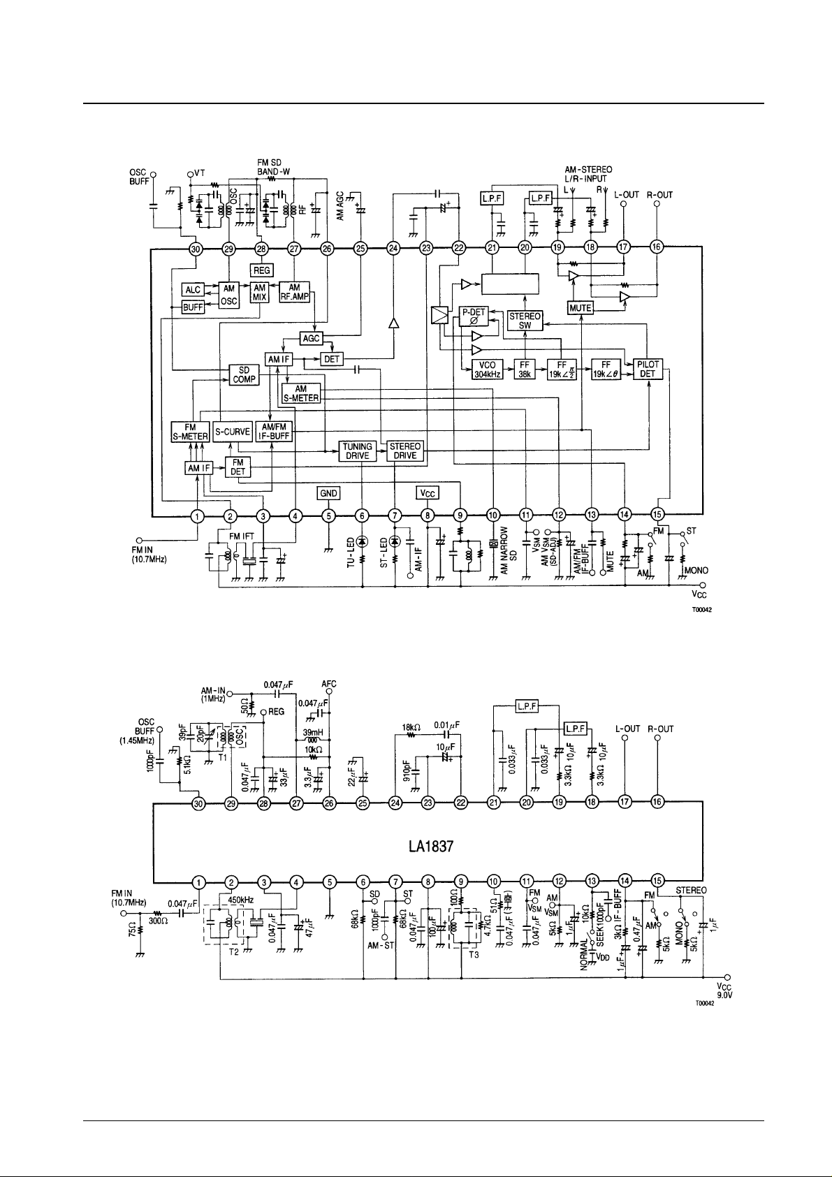
Block Diagram
No. 5688-3/9
LA1837
Test Circuit Diagram
FM SD
ADJ
3 rd 5 th
DECODER
ANTI-BIRDIE
FM
 Loading...