

Page 1
Ordering number : EN4159B
11795TH (OT) No. 4159-1/14
Overview
The LA1835 is an AM, FM IF and MPX single-chip tuner
IC that supports electronic tuning. It was developed
specifically for use in home stereo products and is optimal
for products with auto-seek systems, since it combines SD
and IF counting in its auto-seek implementation.
Furthermore, since the FM detector and MPX VCO
circuits are adjustment free, adoption of the LA1835 can
reduce the number of adjustment steps in the production
line.
Functions
• AM: RF amplifier, mixer, oscillator (with ALC), IF
amplifier, detector, AGC, oscillator buffer,
tuning indicator (narrow-band SD), IF buffer
output, stereo IF output
• FM IF: IF amplifier, quadrature detector, band muting,
tuning indicator, IF buffer output, S-meter
• MPX: PLL stereo decoder, stereo indicator, forced
mono, VCO stop function, adjacent channel
interference rejection function (114 kHz), postamplifier with muting function
Features
• Significant reduction in the number of manufacturing
adjustment steps
FM detector: Adjustment free (using a ceramic
discriminator)
MPX VCO: Adjustment free (using a ceramic
resonator)
• Tuning indicator output provided. (This pin can also be
used as a narrow band stop signal and as a muting drive
output.)
• Adjustable FM stop sensitivity and bandwidth
• Built-in AM local oscillator buffer
• Support for AM low band cut control
• Adjustable AM stop sensitivity
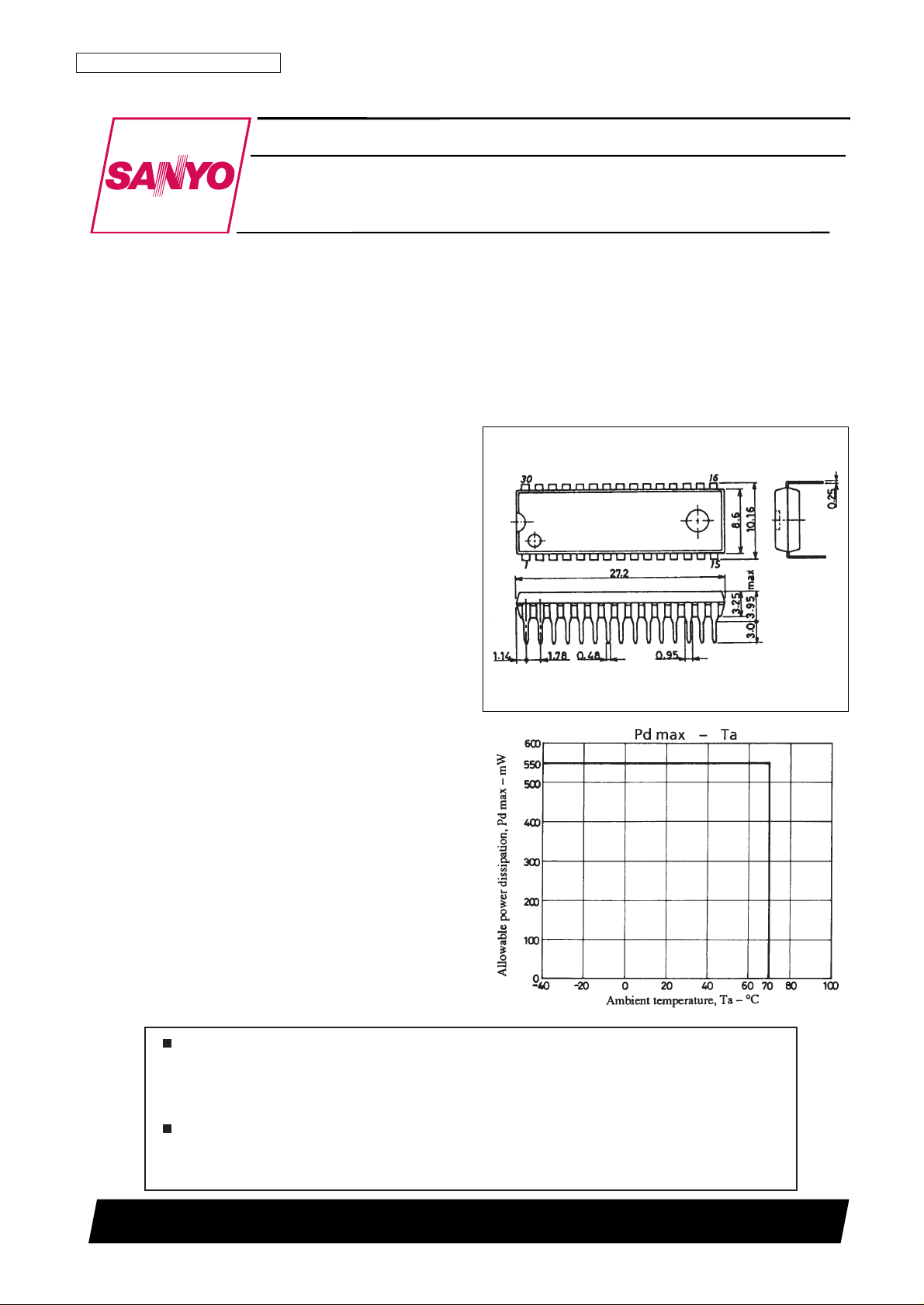
Package Dimensions
unit: mm
3196-DIP30SD
SANYO: DIP30SD
[LA1835]
LA1835
SANYO Electric Co.,Ltd. Semiconductor Bussiness Headquarters
TOKYO OFFICE Tokyo Bldg., 1-10, 1 Chome, Ueno, Taito-ku, TOKYO, 110-8534 JAPAN
Home Stereo Single-Chip Tuner IC
with Electronic Tuning Support
Monolithic Linear IC
Any and all SANYO products described or contained herein do not have specifications that can handle
applications that require extremely high levels of reliability, such as life-support systems, aircraft’s
control systems, or other applications whose failure can be reasonably expected to result in serious
physical and/or material damage. Consult with your SANYO representative nearest you before using
any SANYO products described or contained herein in such applications.
SANYO assumes no responsibility for equipment failures that result from using products at values that
exceed, even momentarily, rated values (such as maximum ratings, operating condition ranges, or other
parameters) listed in products specifications of any and all SANYO products described or contained
herein.
Page 2
Specifications
Maximum Ratings at Ta = 25°C
Operating Conditions at Ta = 25°C
Operating Characteristics
at Ta = 25°C, VCC= 7.0 V, in the specified test circuit using the IC59-3004 socket (Yamaichi Electric Co., Ltd.)
No. 4159-2/14
LA1835
Parameter Symbol Conditions Ratings Unit
Recommended supply voltage V
CC
7.0 V
Operating supply voltage V
CC
op 6.5 to 8.5 V
Parameter Symbol Conditions min typ max Unit
[FM Characteristics (mono): fc = 10.7 MHz, fm = 1 kHz]
Quiescent current I
CCO-FM
No input 23 37 46 mA
Demodulator output V
O-FM
100 dBµ, 100% modulation, the pin 16 output 665 1000 1330 mVrms
Channel balance (monaural) C. B-momo 100 dBµ, 100% modulation, pin 16 output/pin 17 output –1.5 0 +1.5 dB
Total harmonic distortion THD-
FM
100 dBµ, 100% modulation, the pin 16 output 0.3 1.5 %
Signal-to-noise ratio S/N-
FM
100 dBµ, 100% modulation, the pin 16 output 67 74 dB
AM suppression ratio AMR 100 dBµ, 30% AM modulation, the pin 16 output 35 50 dB
Input limiting voltage –3dBL.S 100 dBµ, referenced to 100%, with the input down 3 dB 27 35 dBµ
SD indicator sensitivity SD-on-
FM
47 57 67 dBµ
SD indicator bandwidth SD-
BW
100 dBµ 120 190 280 kHz
IF counter buffer output V
IF Buff-FM
100 dBµ, the pin 11 output 80 120 160 mVrms
V
SM-FM
(1) 0 dBµ, the pin 12 output 0 0.3 1.0 V
S-meter output V
SM-FM
(2) 60 dBµ, the pin 12 output 0.7 1.5 2.5 V
V
SM-FM
(3) 100 dBµ, the pin 12 output 2.5 4.0 5.0 V
Muting attenuation Mute-Att 100 dBµ, 100% modulation, the pin 16 output 80 95 dB
[FM Characteristics (stereo): fc = 10.7 MHz, fm = 1 kHz, L + R = 90%, pilot = 10%, V
IN
= 100 dBµ]
Separation-left Sep-L Left channel modulated; pin 17 output/pin 16 output 30 45 dB
Separation-right Sep-R Right channel modulated; pin 16 output/pin 17 output 30 45 dB
Stereo on level ST-on The pilot modulation such that V7 < 0.7 V 1.8 3.6 6.0 %
Stereo off level ST-off The pilot modulation such that V7 > 4.5 V 2.5 %
Total harmonic distortion (main) THD-main The pin 16 output 0.3 1.5 %
Channel balance (main) C. B-main Pin 16 output/pin 17 output –1.5 0 +1.5 dB
Capture range C. R. Pilot = 10% ±1.5 %
Adjacent channel rejection ratio B. Rej fs = 113 kHz, VS = 90%, pilot = 10%, the pin 16 output 40 dB
[AM Characteristics: fc = 1000 kHz, fm = 1 kHz]
Quiescent current I
CCO-AM
No input 21 29 42 mA
Detector output
V
O-AM
(1) 23 dBµ, 30% modulation, the pin 16 output 25 45 90 mVrms
V
O-AM
(2) 80 dBµ, 30% modulation, the pin 16 output 195 310 490 mVrms
Signal-to-noise ratio
S/N-
AM
(1) 23 dBµ, 30% modulation, the pin 16 output 16 20 dB
S/N-
AM
(2) 80 dBµ, 30% modulation, the pin 16 output 48 54 dB
THD-
AM
(1) 80 dBµ, 30% modulation, the pin 16 output 0.3 1.0 %
Total harmonic distortion THD-
AM
(2) 100 dBµ, 30% modulation, the pin 16 output 0.4 1.2 %
THD-
AM
(3) 80 dBµ, 80% modulation, the pin 16 output 1.0 4.0 %
SD indicator sensitivity SD-on-
AM
20 30 40 dBµ
Local oscillator buffer output V
OSC-AM
No input, the pin 30 output 110 160 mVrms
Low-band attenuation Low-Cut The output for fm = 100 Hz referenced to fm = 1 kHz 5.0 7.0 11.0 dB
IF counter buffer output V
IF Buff-AM
80 dBµ, unmodulated signal, the pin 11 output 140 200 280 mVrms
Stereo IF output V
STIF-AM
80 dBµ, unmodulated signal, the pin 8 output 8.0 17.0 24.0 mVrms
S-meter output
V
SM-AM
(1) 0 dBµ, unmodulated signal 0 0 0.2 V
V
SM-AM
(2) 40 dBµ, unmodulated signal 1.3 3.0 4.5 V
Parameter Symbol Conditions Ratings Unit
Maximum supply voltage V
CC
max 9.0 V
Allowable power dissipation Pd max Ta ≤ 70°C 550 mA
Operating temperature Topr –20 to +70 °C
Storage temperature Tstg –40 to +125 °C
Page 3
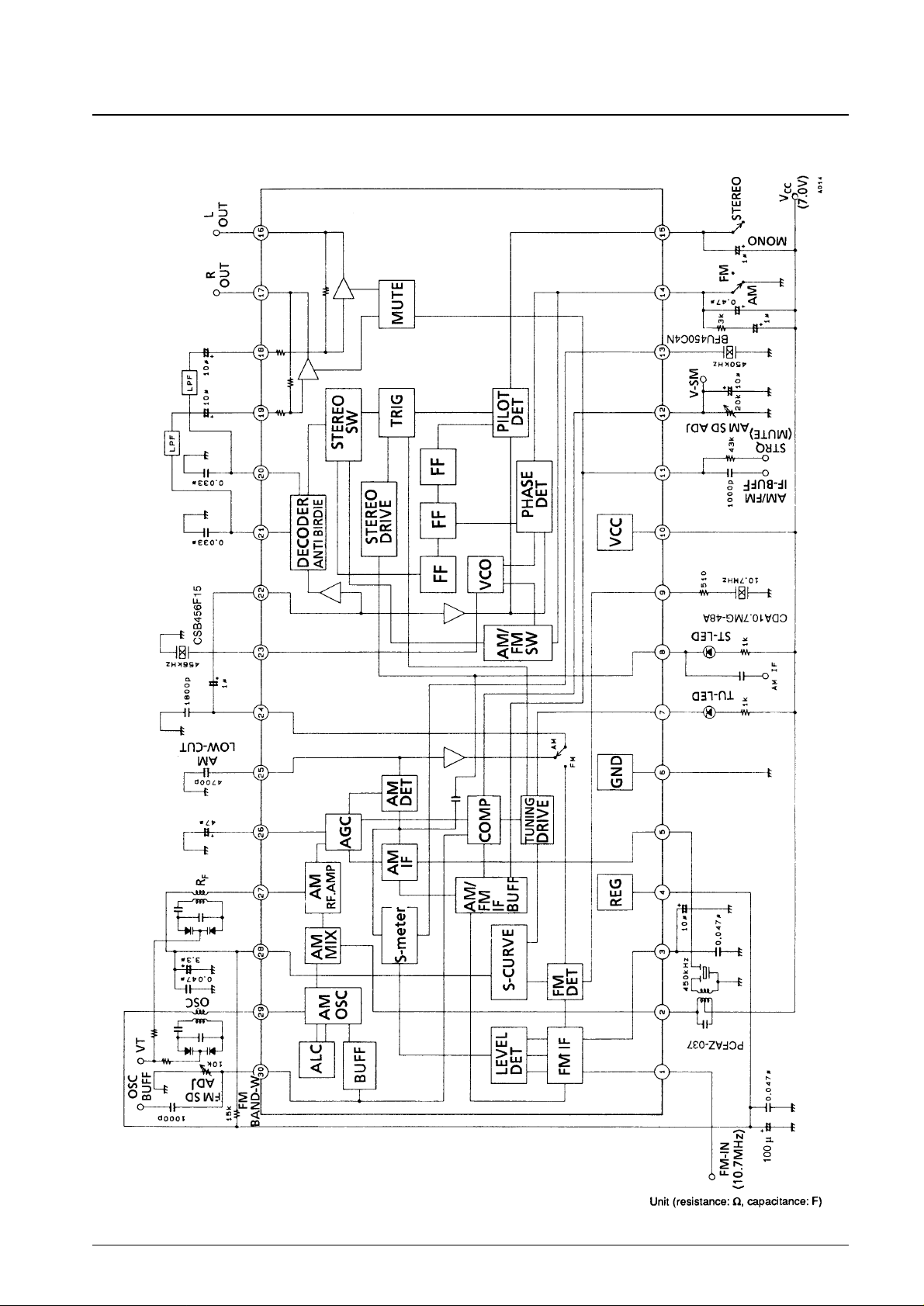
Sample Application Circuit
No. 4159-3/14
LA1835
Page 4
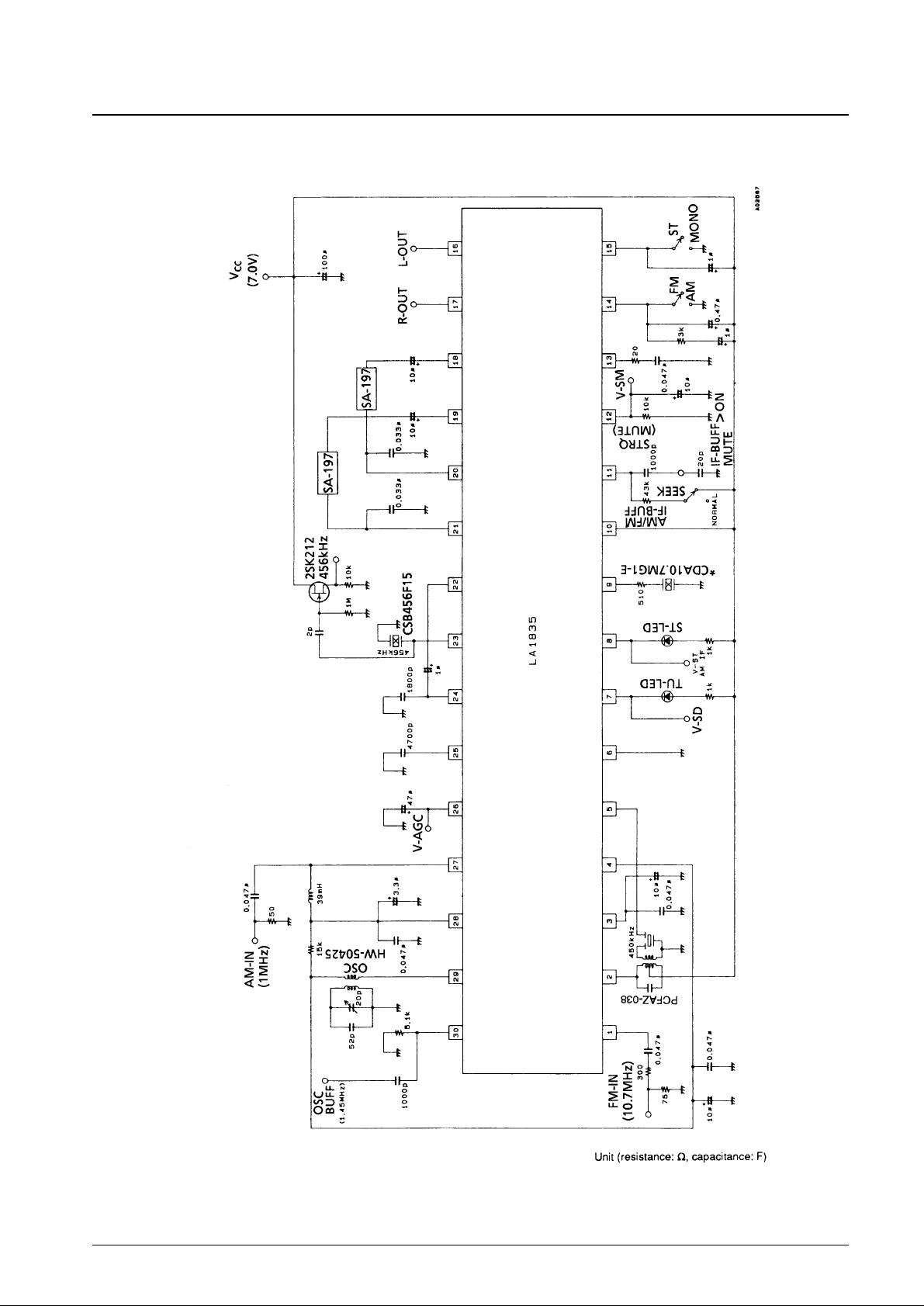
Test Circuit Diagram
Note: Since an IC socket is used, these values differ from those used when the IC is mounted on a printed circuit board.
No. 4159-4/14
LA1835
Page 5
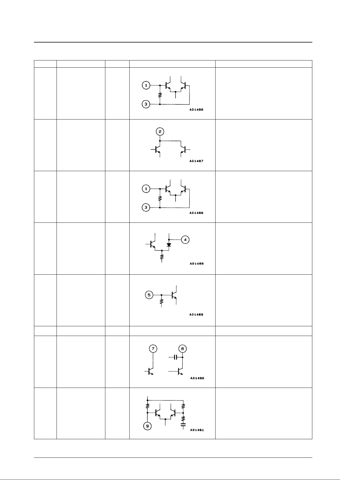
Pin Functions
No. 4159-5/14
LA1835
No. Function Voltage Internal equivalent circuit Note
1
2
3
4
5
6
7
8
9
FM IF input
AM mixer output
FM IF input bypass
REG
AM IF input
GND
Tu-LED
ST-LED
Also functions as the
AM IF output.
FM detector
Vreg
V
CC
Vreg
Vreg
Vreg
0
V
CC
V
CC
2.1 (FM)
2.7 (AM)
Input impedance: ri = 330 Ω
Recommended AM IFT coil:
PCFAZ-037 (Toko Co., Ltd.)
Also used for the AF noise filter.
Vreg = 3.6 V
Input impedance: ri = 2 kΩ
Active low open collector outputs
Pin 8 is used for the AM stereo IF output.
Recommended ceramic discriminator:
CDA 10.7MG-48 (Murata Mfg. Co., Ltd.)
Continued on next page.
Page 6

Continued from preceding page.
No. 4159-6/14
LA1835
No. Function Voltage Internal equivalent circuit Note
10
11
12
13
14
15
16
17
18
19
V
CC
AM/FM IF buffer output
Also functions as the
output control switch
(muting switch).
S-meter output
Also functions as the
AM SD sensitivity
adjustment.
AM narrow band
ceramic filter connection
Phase comparator lowpass filter
(FM/AM switch)
Pilot detector low-pass
filter
(forced mono)
(VCO stop)
Post-amplifier left and
right outputs
Post-amplifier left and
right inputs
V
CC
0
0.3 (FM)
0 (AM)
1.5
VCC– 1.4
(FM)
0 (AM)
V
CC
– 1.0
Vreg
Vreg
Vreg
Vreg
A voltage of 1.3 V or higher turns on the postamplifier output muting. A voltage of 4.0 V or higher
turns on the IF buffer output.
The recommended control voltage for turning
muting on is 1.9 V.
The AM SD sensitivity can be adjusted with the
resistor inserted between this pin and ground.
Since the FM SD sensitivity is affected by this
resistor, the AM SD sensitivity must be adjusted
first.
Recommended narrow band ceramic filter: BFU450
C4N (Murata Mfg. Co., Ltd.)
The LA1835 switches to AM mode when this pin is
connected to ground.
If a current of 50 µA or larger flows from this pin, the
LA1835 switches to mono mode.
The VCO is stopped if this pin is connected to
ground.
Output impedance: ro = 200 Ω
Pin 16: left output
Pin 17: right output
Inverting inputs, ri = 3.3 kΩ
Pin 18: left input
Pin 19: right input
Continued on next page.
Page 7

Continued from preceding page.
No. 4159-7/14
LA1835
No. Function Voltage Internal equivalent circuit Note
20
21
22
23
24
25
26
27
MPX outputs
Left and right outputs
MPX input
MPX VCO
AM/FM demodulator
output
AM low cut
AMAGC
AM RF input
3.5
3.5
2.9
3.5 (FM)
0 (AM)
2.9 (FM)
3.0 (AM)
2.9 (FM)
3.0 (AM)
0 (FM)
0.5 (AM)
Vreg
Output impedance ro = 3.3 kΩ
Pin 20: left de-emphasis
Pin 21: right de-emphasis
Input impedance ri = 20 kΩ
Increasing the value of the external capacitor
connected between this pin and pin 24 improves
the low frequency separation characteristics.
However, the impulse noise associated with
switching between AM and FM also increases.
Recommended ceramic oscillator: CSB456F15
(Murata Mfg. Co., Ltd.)
Output impedances
FM: ro = 250 Ω
AM: ro = 10 kΩ
The separation can be adjusted by changing the
value of the external capacitor connected between
this pin and ground.
The low-band frequency characteristics of the AF
demodulator can be adjusted by changing the value
of the external capacitor connected between this
pin and ground. The AM detector output can be
attenuated by adding a resistor in series with the
capacitor.
The internal load resistance, R is 6.7 kΩ.
Pin 27 must be used at the same voltage as pin 4,
the regulator voltage.
Continued on next page.
Page 8

Continued from preceding page.
No. 4159-8/14
LA1835
No. Function Voltage Internal equivalent circuit Note
28
29
30
AFC
OSC
Oscillator buffer output
Also functions as the
FM SD sensitivity
adjustment.
Vreg
Vreg
1.6 (FM)
1.3 (AM)
The FM SD bandwidth can be adjusted by changing
the value of the external resistor inserted between
pin 28 and pin 4, the regulator voltage.
The oscillator coil is connected between pin 29 and
pin 4, the regulator voltage.
The FM SD sensitivity can be adjusted by changing
the value of the external resistor inserted between
this pin and ground. The AM SD sensitivity must be
adjusted before the AM FD sensitivity.
Output impedance ro = 200 Ω
Page 9

No. 4159-9/14
LA1835
Page 10

No. 4159-10/14
LA1835
Page 11

No. 4159-11/14
LA1835
Page 12

No. 4159-12/14
LA1835
Page 13

No. 4159-13/14
LA1835
Page 14

PS No. 4159-14/14
LA1835
This catalog provides information as of August, 1998. Specifications and information herein are subject to
change without notice.
Specifications of any and all SANYO products described or contained herein stipulate the performance,
characteristics, and functions of the described products in the independent state, and are not guarantees
of the performance, characteristics, and functions of the described products as mounted in the customer’s
products or equipment. To verify symptoms and states that cannot be evaluated in an independent device,
the customer should always evaluate and test devices mounted in the customer’s products or equipment.
SANYO Electric Co., Ltd. strives to supply high-quality high-reliability products. However, any and all
semiconductor products fail with some probability. It is possible that these probabilistic failures could
give rise to accidents or events that could endanger human lives, that could give rise to smoke or fire,
or that could cause damage to other property. When designing equipment, adopt safety measures so
that these kinds of accidents or events cannot occur. Such measures include but are not limited to protective
circuits and error prevention circuits for safe design, redundant design, and structural design.
In the event that any and all SANYO products described or contained herein fall under strategic
products (including services) controlled under the Foreign Exchange and Foreign Trade Control Law of
Japan, such products must not be exported without obtaining export license from the Ministry of
International Trade and Industry in accordance with the above law.
No part of this publication may be reproduced or transmitted in any form or by any means, electronic or
mechanical, including photocopying and recording, or any information storage or retrieval system,
or otherwise, without the prior written permission of SANYO Electric Co., Ltd.
Any and all information described or contained herein are subject to change without notice due to
product/technology improvement, etc. When designing equipment, refer to the “Delivery Specification”
for the SANYO product that you intend to use.
Information (including circuit diagrams and circuit parameters) herein is for example only; it is not
guaranteed for volume production. SANYO believes information herein is accurate and reliable, but
no guarantees are made or implied regarding its use or any infringements of intellectual property rights
or other rights of third parties.
 Loading...