

Page 1
Ordering number : ENN*6854
Preliminary
LA1823
Monolithic Linear IC
LA1823
Single-Chip Tuner IC
for Use in Radio Cassette Recorder
Overview
The LA1823 is a single-chip tuner IC that incorporates
FM/AM and MPX circuits and supports electronic tuning.
The built-in MPX-VCO allows this IC to be adjustment-free
and to require no external components.
Features
•
FM, AM and MPX integrated in a single-chip.
• FM front-end : Local OSC voltage reduced.
• Adjustment free MPX-VCO
: No ceramic resonator used.
• Adjustment free FM-DET
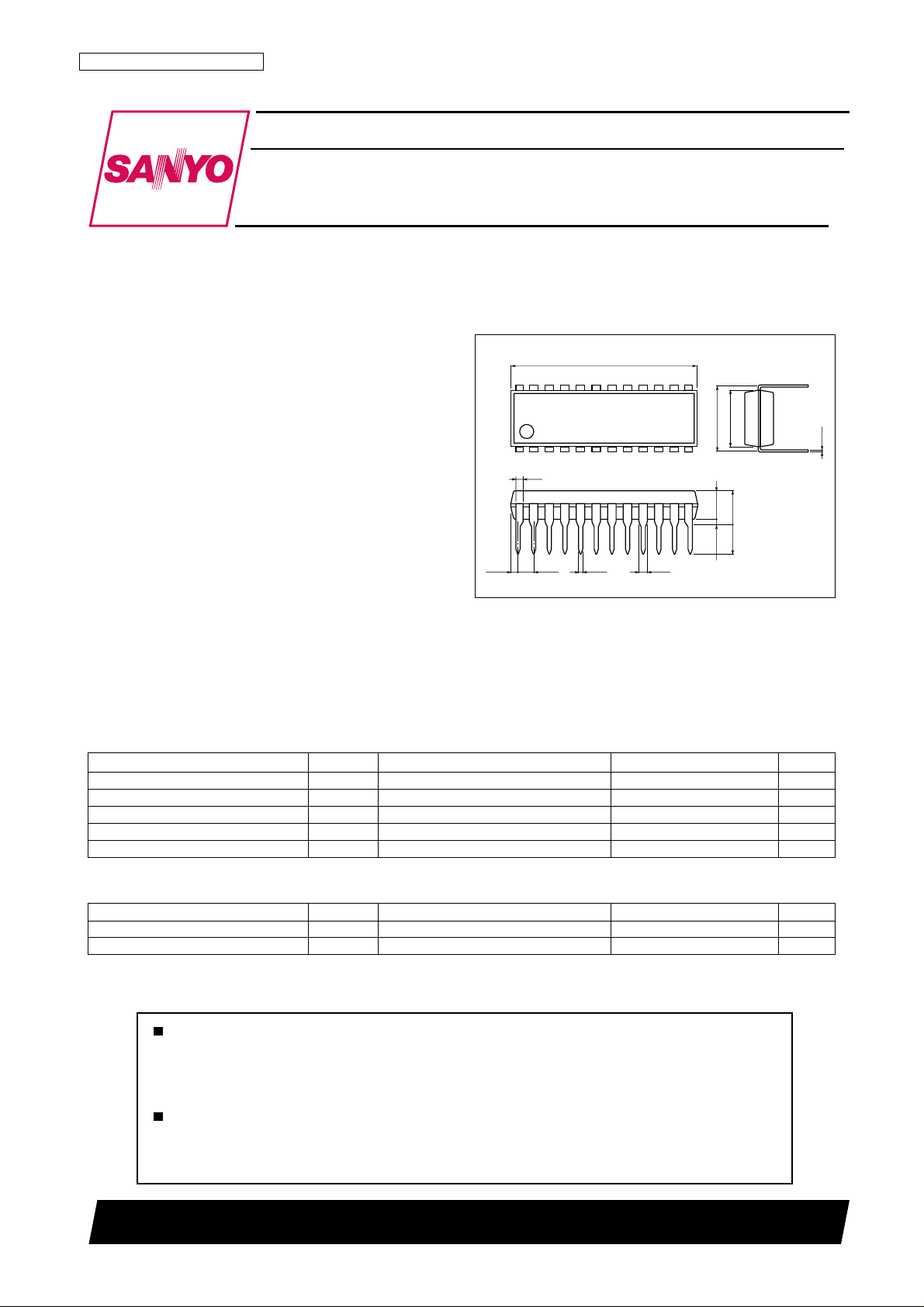
Package Dimensions
unit : mm
3067A
[LA1823]
21.0
24
1
0.9
13
12
: Using ceramic discriminator.
• Build in FM stereo indicator.
• Build in FM/AM IF count buffer.
• Build in AM OSC buffer.
• Package : DIP-24S.
(0.71)
1.78
0.48
0.95
SANYO : DIP-24S(300mil)
Functions
FM : RF amplifier, mixer , oscillator, IF amplifier, detector, signal meter, IF count buffer output.
AM : RF amplifier, mixer, oscillator (with ALC), oscillator buffer output, IF amplifier, detector, AGC,
IF count buffer output.
MPX : PLL stereo decoder, stereo indicator, VCO on chip, forced monaural, Audio mute.
Specifications
Maximum Ratings at Ta = 25 °C
6.4
7.62
(3.25)
3.9max
0.51min
0.25
3.3
Parameter Symbol Conditions Ratings Unit
Maximum supply voltage VCC max 7.0 V
Indicator drive current I
Allowable power dissipation Pd max Ta ≤ 70 °C 300 mW
Operating temperature Topg --20 to +70 °C
Storage temperature Tstg --40 to +125 °C
LED
Pin 8 20 mA
Operating Conditions at Ta = 25 °C
Parameter Symbol Conditions Ratings Unit
Recommended supply voltage V
Operation supply voltage range VCC op 1.8 to 6.0 V
Any and all SANYO products described or contained herein do not have specifications that can handle
applications that require extremely high levels of reliability, such as life-support systems, aircraft's
control systems, or other applications whose failure can be reasonably expected to result in serious
physical and/or material damage. Consult with your SANYO representative nearest you before using
any SANYO products described or contained herein in such applications.
SANYO assumes no responsibility for equipment failures that result from using products at values that
exceed, even momentarily, rated values (such as maximum ratings, operating condition ranges, or other
parameters) listed in products specifications of any and all SANYO products described or contained
herein.
CC
4.5 V
SANYO Electric Co.,Ltd. Semiconductor Company
TOKYO OFFICE Tokyo Bldg., 1-10, 1 Chome, Ueno, Taito-ku, TOKYO, 110-8534 JAPAN
11201 RM (IM)
No.6854-1/10
Page 2
LA1823
Operating Characteristics at Ta = 25 °C, V
= 4.5 V, in the specified test circuit using
CC
the IC59-2043-2 socket (Yamaichi Electric Co.,Ltd.)
Quiescent supply current
Parameter Symbol Conditions
FM-mode quiescent current ICC(FM) No input 10.0 15.0 20.0 mA
AM-mode quiescent current ICC(AM) No input 6.5 9.2 14.5 mA
min typ max
Ratings
Unit
FM front-end characteristics at fc = 98 MHz, fm = 1 kHz, 22.5 kHz dev
Parameter Symbol Conditions
Input limiting voltage --3 dB L.S.
Local oscillator voltage V
OSC
min typ max
Referenced to VIN = 60 dBµV EMF,
22.5 kHz dev, a 3 dB down input
fosc = 108.7 MHz
with FET buffer gain ·=· 0 dB
Ratings
12 dBµV EMF
100 mVrms
Unit
FM IF characteristics (monaural) at fc = 10.7 MHz, fm = 1 kHz, 75 kHz dev
Parameter Symbol Conditions
Demodulation output V
Signal-to-noise ratio S/N VIN = 100 dBµV6372dB
Total harmonic distortion (mono) THD VIN = 100 dBµV 0.5 1.5 %
Input limiting voltage --3 dB L.S.
IF count buffer on level IF buff on IF count buffer on 35 45 55 dBµV
IF count buffer output V
IF buff
VIN = 100 dBµV 135 180 240 mVrms
O
Referenced to V
75 kHz dev, a 3 dB down input
Test from pin 7 for
VIN = 100 dBµV, no modulation
= 100 dBµV,
IN
min typ max
Ratings
31 38 45 dBµV
120 180 240 mVrms
Unit
FM IF characteristics (stereo) at fc = 10.7 MHz, fm = 1 kHz, 75 kHz dev, L + R = 90 %, PILOT = 10 %
Parameter Symbol Conditions
Separation SEP VIN = 100 dBµV2540dB
Stereo on level ST-ON VIN = 100 dBµV, Pilot modulation 2.4 3.5 7.2 %
Total harmonic distortion (main) THD VIN = 100 dBµV 0.5 1.7 %
min typ max
Ratings
Unit
AM characteristics at fc = 1 MHz, fm = 1 kHz, mod = 30 %
Parameter Symbol Conditions
Detector output
Signal-to-noise ratio
Total harmonic distortion THD V
OSC buffer output V
IF count buffer on level IF buff on IF count buffer on 15 25 32 dBµV
IF count buffer output V
VO(1) V
VO(2) V
S/N(1) V
S/N(2) V
buff Test from pin 8 for no input 80 100 160 mVrms
OSC
IF buff
= 23 dBµV 17 30 53 mVrms
IN
= 80 dBµV 50 75 120 mVrms
IN
= 23 dBµV1520dB
IN
= 80 dBµV4754dB
IN
= 80 dBµV 0.5 1.5 %
IN
Test from pin 7 for
VIN = 80 dBµV, no modulation
min typ max
Ratings
110 180 220 mVrms
Unit
No.6854-2/10
Page 3
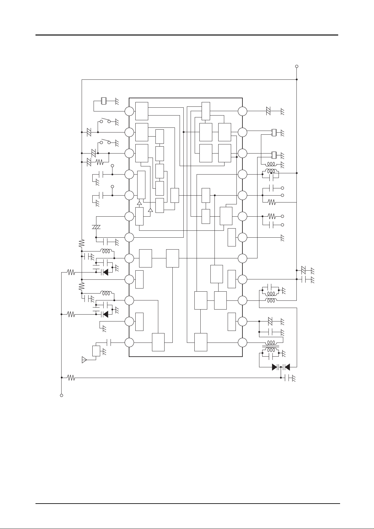
Block Diagram
LA1823
V
CC
FM
ST
MONO
FM
AM
+
+ +
R-OUT L-OUT
+
DET
DET
PILOT
COMP
PHASE
DECODER
MUTEV
FM
OSC
2GND2
CC
FF FFFF
VCO
ST SW
FM
TRIG
MIX
AGC
AM
DET
FM
S-METER
ST
SD
OSC
BUFFER
AM
FM
IF
IF
IF
BUFFER
1 GND1
CC
+
450kHz
10.7MHz
Buff
AM OSC
ST
Mute
IF Buff
AM / FM
+
Vtune
FM Ant
BPF
AM
24 23 22 21 20 19 18 17 16 15 14 13
FM
RF
AM
MIX
RF
AM
OSC
REG V
1 2 3 4 5 6 7 8 9 10 11 12
+
AM Ant
ILA00300
No.6854-3/10
Page 4

Sample Application Circuit Diagram
FM-DET
ST
3.3µF
MONO
FM
AM
+
0.22µF
+ +
BUFF
FM OSC
3pF
1000pF
1.2kΩ
10Ω10Ω
33kΩ33kΩ33kΩ
0.047µF0.047µF
2SC2999
220kΩ
100Ω
1000pF
0.47µF
2700pF
pF
1000
pF
1000
3.3kΩ
6800pF6800pF
+
SVC201
SVC201
L-OUT
R-OUT
4.7µF
FM-OSC
FM-RF
8pF
12pF
FM
DET
DET
PILOT
COMP
PHASE
DECODER
MUTE
FM
OSC
2
CC
V
GND2
LA1823
FF FFFF
VCO
TRIG
ST SW
FM
MIX
AM
AM
FM
MIX
AGC
DET
S-METER
ST
SD
OSC
IF
AM
IF
FM
IF
BUFFER
AM
OSC
BUFFER
GND1
1
CC
V
REG
470pF
+
100pF
10kΩ
100pF
+
22µF
AM-MIX
kΩ
100
22pF
AM-OSC
10µF
CC
V
450kHz
Buff
AM OSC
ST
SEEK
IF Buff
AM / FM
10.7MHz
100µF
+
0.047µF
Vtune
FM Ant
BPF
1000pF
8pF
0.047µF
SVC348
0.047µF
100kΩ
ILA00301
24 23 22 21 20 19 18 17 16 15 14 13
FM
RF
AM
RF
1 2 3 4 5 6 7 8 9 10 11 12
AM Ant
10
pF
No.6854-4/10
Page 5

LA1823
2
ACFA-450L08
GND
ILA00305
3
1
S
V
CC
S
4
6
Pin9
Coil specifications (bottom view)
• FM-BPF : SA-309 (Sumida) 88 MHz to 108 MHz
• FM-RF : SA-149 (Sumida) 3.6 mm diameter, air core, 0.6 mm wire, 4.5 T
• FM-OSC : SA-151 (Sumida) 3.6 mm diameter, air core, 0.6 mm wire, 3.5 T
• FM-IF filter, discriminator :
SK107M1-AE-10, CDF107F-AE-029 (Toko)
SFE10.7MA5, CDA10.7MG1-A (Murata) : tentative
• AM-OSC : SA-181 (Sumida) : L7BRS-3132AQ (Toko)
S
3
VC
2
1
GND
• AM-MIX : SA-1136 (Sumida) : PCFAZ-082 (Toko)
S
3
V
2
CC
Pin9
1
4
Pin3
6
V
S
ILA00302
S
4
CF
6
GND
CC
6-4 37 T 3-1 64 T
3-1 74 T 6-4 32 T
0.06UEW 0.06-2UEW
fo = 796 kHz fo = 796 kHz
Qo ≥ 80 Qo ≥ 65
L = 140 µH L = 140 µH
3-2 122 T 1-2 47 T
4-6 9 T 2-3 100 T
2-1 62 T 4-6 12 T
0.06UEW fo = 450 kHz
fo = 450 kHz, Qo ≥ 65 180 pF internal
180 pF internal With AM-IF filter
ILA00304
• AM-IF filter : SFU450B (Murata)
• MW Bar-antenna : C8E-A0105 (Toko)
1-2 67 T
3-4 9 T
2
S
3
4
Pin1GNDVC Pin2
ILA00306
fo = 796 kHz
Qu = 180 min
L = 260µH
S
1
VC
GND
S
3
2
1
4
6
S
ILA00302
Pin3
V
CC
No.6854-5/10
Page 6

LA1823
Pin Descriptions and Quiescent Voltage at VCC = 4.5 V
Pin
number
Function voltage (V) Equivalent circuit Remarks
Quiescent
AM FM
2
1 AM-RF input 1.2 1.2
2 Reg 1.2 1.2
3 AM-OSC 4.5 4.5
1
2
3 4
Connect the AM antenna coil
between this pin and pin 2 (Reg)
ILA00307
ILA00308
Connect the AM oscillator coil
between this pin and pin 4
(VCC1)
ILA00309
4VCC1 4.5 4.5 AM/FM-IF/MPX block V
5 FM-MIX output 2.4 2.2 Rout = 270 Ω
5
Rout
ILA00310
CC
6 GND1 0 0 AM/FM-IF/MPX block ground
IF buffer
7 output and 4.5 4.5
mute switch
7
ILA00311
V7 ≥ 1.3 V : IF buffer output and
muting on
No.6854-6/10
Page 7

LA1823
Pin
number
8
Function voltage (V) Equivalent circuit Remarks
Stereo
indicator,
AM-oscillator
buffer output
Quiescent
AM FM
4.5 4.5
8
Active-low
Open-collector output
AM oscillator signal is output in
AM mode
ILA00312
9
4
Connect the AM mixer coil
9 AM-MIX output 4.5 4.5
between this pin and pin 4
(VCC1)
ILA00313
10
10 FM-IF input 1.2 1.2 Rin = 330 Ω
2
Rin
ILA00314
11
11 AM-IF input 1.2 1.2 Rin = 2 kΩ
2
Rin
ILA00315
AM-AGC
output and
12
FM signal R = 16.6 kΩ
0.4 0.1
12
R
Internal load resistance
meter output
ILA00316
Recommended ceramic
13 FM-DET 3.9 3.7
13
discriminator :
CDF107F-AE-029 (T oko)
CDA10.7MG** (Murata)
ILA00317
No.6854-7/10
Page 8

LA1823
Pin
number
Function voltage (V) Equivalent circuit Remarks
Pilot detector
14 filter 2.9 3.8
(forced mono)
Quiescent
AM FM
14
Forced monaural mode when pin
14 is connected to ground
ILA00318
15
Phase FM mode is when pin 15 is open,
15 comparator filter 0 3.8 and AM mode is when pin 15 is
(AM/FM switch) connected to ground
ILA00319
16 L output
17 R output
1.2 1.2 Rout = 7.5 kΩ
Rout
16
17
( )
ILA00320
18
18 MPX input 1.2 1.2 Rin = 50 kΩ
Rin
ILA00321
Output impedance
AM : Rout = 50 kΩ
AM/FM
19 detector 0.3 1.0
output
Rout(FM)
19
Rout(AM)
ILA00322
21 20
FM : Rout = 500 Ω
The channel separation can be
adjusted with an external
capacitor connected between this
pin and ground
Connect the FM oscillator coil
20 FM-OSC 4.5 4.4 between this pin and pin 21
(VCC2)
ILA00323
No.6854-8/10
Page 9

LA1823
Pin
number
Function voltage (V) Equivalent circuit Remarks
21 VCC2 4.5 4.4 Power is supplied from pin 4
Quiescent
AM FM
R
421
FM-FE block V
CC
(VCC1) via external resistor
ILA00324
22 21
FM-RF 4.5 4.4 Connect the FM-RF coil between
22
output this pin and pin 21 (VCC2)
24 FM-RF input 0 0.9
24
Rin
ILA00325
(10 Ω)
Rin = 1.8 kΩ
23 GND2 0 0 FM-FE block ground
0
--20
--40
FM Characteristics
Signal
AM out
--60
Output -- dBm
VCC=4.5V
--80
fc=98MHz
Noise
fm=1kHz, 22.5kHz dev
AM=30%mod
--100
--20 40200 60 10080 120 140
Ant input -- dBµV EMF
0
VCC=4.5V
AM Characteristics
fc=1000kHz
fm=1kHz, 30%mod
--20
--40
--60
Output -- dBm
Signal
Noise
--80
ILA00326
5
FM Characteristics
VCC=4.5V
fc=98MHz
fm=1kHz
THD -- %
4
3
2
1
THD(75k)
0
--20 40200 60 10080 120 140
THD(22.5k)
Ant input -- dBµV EMF
5
AM Characteristics
VCC=4.5V
fc=1000kHz
4
fm=1kHz, 30%mod
THD30%
3
2
THD -- %
1
VAGC
THD80%
ILA00327
2.5
2.0
1.5
1.0
0.5
VAGC -- V
--100
--20 40200 60 10080 120 140 --20 40200 60 10080 120 140
Ant input -- dB/m
ILA00328
0
Ant input -- dB/m
ILA00329
No.6854-9/10
0
Page 10

LA1823
Sep -- dB
60
FM st Characteristics
VCC=4.5V
fc=98MHz, Vin=60dBµV EMF
50
75kHz dev, L+R=90%
Pilot=10%
40
Sep R
Sep L
30
20
10
0
fm -- kHz
1000.01 0.1 1.0 10
ILA00330
5
VCC=4.5V
fc=98MHz, Vin=60dBµV EMF
75kHz dev, L+R=90%
4
Pilot=10%
3
2
THD -- %
1
0
FM st Characteristics
Sub
ST
fm -- kHz
Main
Mono
1000.01 0.1 1.0 10
ILA00303
Specifications of any and all SANYO products described or contained herein stipulate the performance,
characteristics, and functions of the described products in the independent state, and are not guarantees
of the performance, characteristics, and functions of the described products as mounted in the customer's
products or equipment. To verify symptoms and states that cannot be evaluated in an independent device,
the customer should always evaluate and test devices mounted in the customer's products or equipment.
SANYO Electric Co., Ltd. strives to supply high-quality high-reliability products. However, any and all
semiconductor products fail with some probability. It is possible that these probabilistic failures could
give rise to accidents or events that could endanger human lives, that could give rise to smoke or fire,
or that could cause damage to other property. When designing equipment, adopt safety measures so
that these kinds of accidents or events cannot occur. Such measures include but are not limited to protective
circuits and error prevention circuits for safe design, redundant design, and structural design.
In the event that any or all SANYO products(including technical data,services) described or
contained herein are controlled under any of applicable local export control laws and regulations,
such products must not be exported without obtaining the export license from the authorities
concerned in accordance with the above law.
No part of this publication may be reproduced or transmitted in any form or by any means, electronic or
mechanical, including photocopying and recording, or any information storage or retrieval system,
or otherwise, without the prior written permission of SANYO Electric Co. , Ltd.
Any and all information described or contained herein are subject to change without notice due to
product/technology improvement, etc. When designing equipment, refer to the "Delivery Specification"
for the SANYO product that you intend to use.
Information (including circuit diagrams and circuit parameters) herein is for example only ; it is not
guaranteed for volume production. SANYO believes information herein is accurate and reliable, but
no guarantees are made or implied regarding its use or any infringements of intellectual property rights
or other rights of third parties.
This catalog provides information as of January, 2001. Specifications and information herein are subject to
change without notice.
No.6854-10/10
PS
 Loading...