

Page 1
Any and all SANYO products described or contained herein do not have specifications that can handle
applications that require extremely high levels of reliability, such as life-support systems, aircraft’s
control systems, or other applications whose failure can be reasonably expected to result in serious
physical and/or material damage. Consult with your SANYO representative nearest you before using
any SANYO products described or contained herein in such applications.
SANYO assumes no responsibility for equipment failures that result from using products at values that
exceed, even momentarily, rated values (such as maximum ratings, operating condition ranges,or other
parameters) listed in products specifications of any and all SANYO products described or contained
herein.
Monolithic Linear IC
150mA, 5V 5-Pin Voltage Regulator
with Reset Function
Ordering number:ENN2622B
L78LR05
SANYO Electric Co.,Ltd. Semiconductor Company
TOKYO OFFICE Tokyo Bldg., 1-10, 1 Chome, Ueno, Taito-ku, TOKYO, 110-8534 JAPAN
6.5
2.3
0.5
1.2
0.5
0.5
1.3 1.3 1.3 1.3
0.6
5.0
1.55.5
7.0
7.5
Overview
The L78LR05 is voltage regulator IC that performs the reset signal generating function when the power supply of a
microcomputer system is turned ON/OFF. The L78LR05
is convenient for battery backup system at the time of po wer
failure. The reset threshold voltage VRT is ranked as shown
below.
V
TR
VTR)V(8.45.42.49.36.33.30.3
Applications
• Prevention of malfunction that may occur when the pow er
supply of a microcomputer is turned ON/OFF.
• Measures taken against abnormal operations that may
occur at the time of instantaneous break of power supply.
• Direct battery backup for SRAM.
knarBCDEFGH
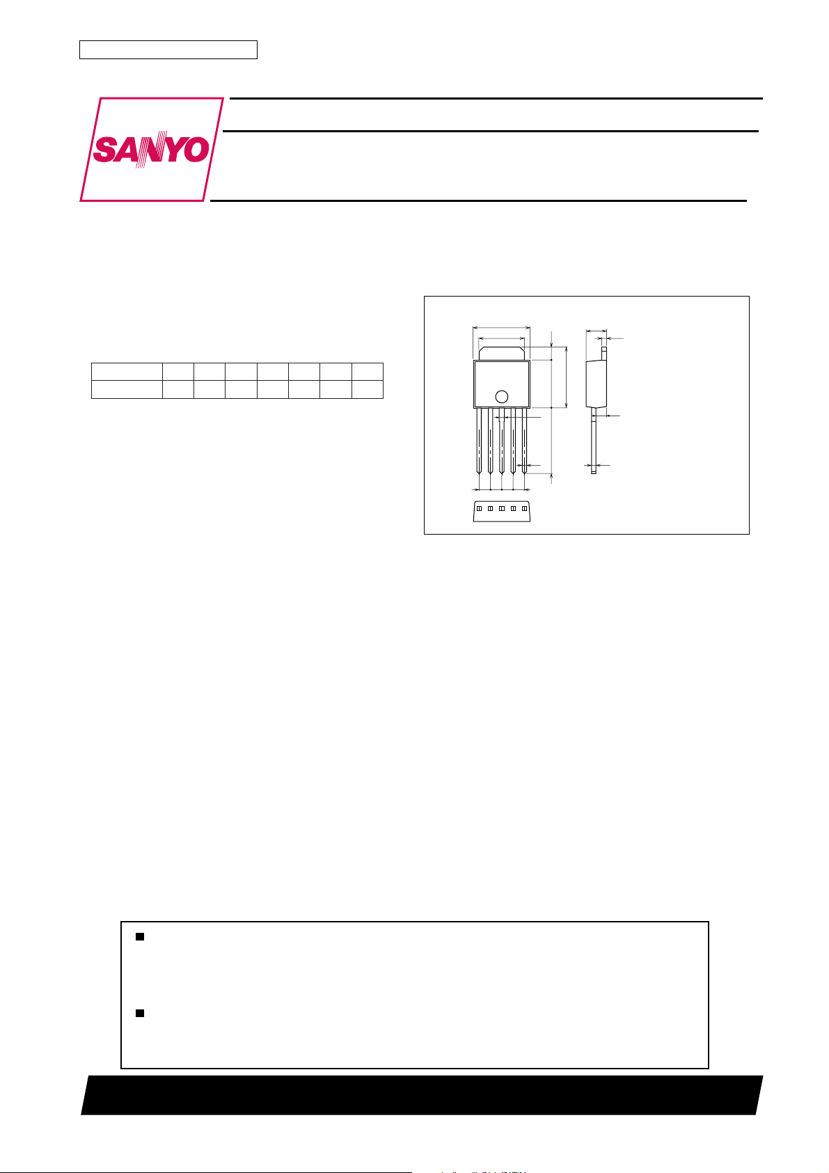
Package Dimensions
unit:mm
3103
[L78LR05]
1 : INPUT
2 : DELAY CAPACITOR
3 : GND
4 : RESET OUTPUT
5 : OUTPUT
SANYO : TP-5H
Features
• 5V, 150mA output.
• Capable of generating a microcomputer reset signal.
• No battery-regulator switching circuit required at the battery backup mode (Output leakage current : 2µA or less).
• An external capacitor can be used to set the reset output
delay time.
• Applicable to the po wer supply of CMOS , NMOS microcomputers.
• Especially suited for use as an on-board regulator for a
microcomputer system.
• Small-sized power package TP-5H permitting the equipment to be made compact.
• The allowable power dissipation can be increased by being surface-mounted on the board.
• Capable of being mounted in a variety of methodes because of various lead forming versions available.
• On-chip protectors (overcurrent limiter, ASO protector,
thermal protector).
D1599TH (KT)/61093TS/8039YT/5178TA/7067TA, TS No.2622–1/6
Page 2
Specifications
Maximum Ratings at Ta = 25˚C
retemaraPlobmySsnoitidnoCsgnitaRtinU
egatloVtupnImumixaMV
noitapissiDrewoPelbawollAxamdP)nifoN( 0.1W
erutarepmeTgnitarepOrpoT 08+ot03–
erutarepmeTegarotSgtsT 051+ot55–
Operating Conditions at Ta = 25˚C
retemaraPlobmySsnoitidnoCsgnitaRtinU
egatloVtupnIV
tnerruCtuptuOI
L78LR05
xam 52V
NI
NI
TUO
02ot5.7V
051ot1Am
˚C
˚C
Operating Characteristics at Ta = 25˚C, VIN=10V, I
retemaraPlobmySsnoitidnoC
egatloVtuptuO
noitalugeReniL
noitalugeRdaoL
noitapissiDtnerruCI
noitairaVnoitapissiDtnerruC
egatloVesioNtuptuOV
egatloVtuptuOfotneieiffeoCerutarepmeT
noitcejeRelppiRjerR 97Bd
egatloVtuoporDV
tnerruCtrohStuptuOI
egatloVtuptuOteseR-"H"V
egatloVtuptuOteseR-"L"V
egatloVdlohserhTteseRV
egatloVsiseretsyHdlohserhTteseRV
emiTyleDtuptuOteseRt
tnerruCegakaeLniPtuptuOI
tnerruCegakaeLniPtuptuOteseRI
V
V
∆V
∆V
∆V
∆V
∆I
∆I
∆V
Tj=25°C
1TUO
V7 ≤VNI≤ Am1,V02 ≤I
2TUO
Tj=25°C, 7V≤VIN≤20V
1ENILo
Tj=25°C, 8V≤VIN≤20V
2ENILo
Tj=25°C, 1mA≤I
1DAOLo
Tj=25°C, 1mA≤I
2DAOLo
Tj=25°C, I
CC
V8 ≤VNI≤ V0221.05.1Am
ENILCC
Am1 ≤I
DAOLCC
ON
/∆ jT
TUO
CSO
HRO
LRO
TR
HTR
d
zH01 ≤f≤ I,zHk001
I
=1mA, Tj=25 to 125°C
OUT
Tj=25°C, f=120Hz, 8V≤VIN≤18V
Tj=25°C
PORD
Tj=25°C
Tj=25°C
Tj=25°C, VIN=3V, Io=1mA
B, Tj=25°C
C, Tj=25°C
D, Tj=25°C
E, Tj=25°C
F , Tj=25°C
G, Tj=25°C
H, Tj=25°C
c
d
VNIV,0=
KAELO
VNIV,0=
KAELRO
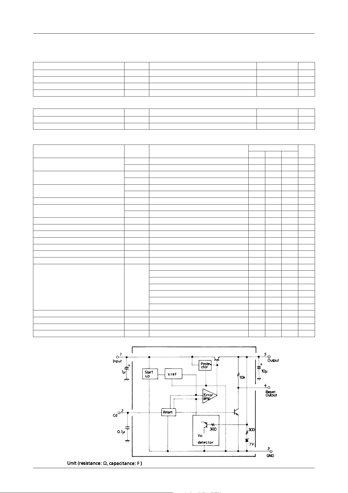
Equivalent Circuit Block Diagram
=40mA, cin=1µF, co=10µF
OUT
sgnitaR
nimpytxam
8.40.52.5V
≤ Am0757.452.5V
TUO
≤100mA
OUT
≤40mA
OUT
=100mA
OUT
≤ Am0410.01.0Am
TUO
Fµ1.0=5.7015.21sm
V6=100.02Aµ
o
RO
Am1=08Vµ
o
V6=100.02A
0.657Vm
0.305Vm
0.906Vm
0.303Vm
4.14.3Am
5.0±
5.12.2V
051003054Am
8.40.52.5V
01002Vm
06.48.459.4V
03.45.456.4V
00.42.453.4V
07.39.350.4V
04.36.357.3V
01.33.354.3V
08.20.351.3V
05001002Vm
mV/˚C
tinU
No.2622–2/6
Page 3

L78LR05
Sample Application Circuit 1
Note 1 : When the capacitance of Cd is large, the capacitor may not discharge completely, causing td to be made shorter than a set value. If this is a
problem, either connect a high speed diode (DS442) between pin2 (anode side) and pin5 (cathode side) or ensure an adequate discharge time by
using values for capacitors Cin and Cd such that Cin>Cd.
Note 2 : If a pull-up resistor is connected to the reset output pin externally, it is possible to cause a sink current up to 4mA to flow.
Reset Operation
Sample Application Circuit 2 (Direct battery backup)
Since the leakage current at the output pin (pin5) of the L78LR05 is so low as 2µA or less, a backup circuit can be
implemented by connectiong an electric double layer capacitor (super capacitor : NEC, gold capacitor : Matsushita Electric) or a Ni Cd battery direct to the output pin. Since a reverse blocking diode, which has been so far connected to the
output pin, is not required, a regulated power-supply voltage can be supplied to a load during the steady-state operation,
without voltage drop caused by the diode and effects of temperature characteristics, current characteristics of the diode. No
battery-regulator switching circuit is required at the battery backup start mode.
Note 3 : The capacitance of reset output signal delay capacitor Cd must exceed that of input capacitor Cin. If the capacitance of Cd is small, a reset pulse
signal may be generated once when the main power source is turned off (at the battery backup start mode).
No.2622–3/6
Page 4

L78LR05
Allowable Power Dissipation
The allowable power dissipation is 1.0V (Ta=25°C) with fin attached. When the L78LR05 is surface-mounted on a
hybrid IC board or printed circuit board, a high allowable power dissipation can be obtained, though it is placed in a
small-sized package. Shown below is the relationship between the Cu-foiled area the allowable power dissipation
when the L78LR05 is surface-mounted on a glass epoxy boad (50×50×0.8mm3).
* The measured values of Pd represent the values measured
when solder on the Cu-foiled area is all wet.
Lead Forming
MA forming
FA forming
LR forming
No.2622–4/6
Page 5

L78LR05
No.2622–5/6
Page 6

L78LR05
Specifications of any and all SANYO products described or contained herein stipulate the performance,
characteristics, and functions of the described products in the independent state, and are not guarantees
of the performance, characteristics, and functions of the described products as mounted in the customer's
products or equipment. To verify symptoms and states that cannot be evaluated in an independent device,
the customer should always evaluate and test devices mounted in the customer's products or equipment.
SANYO Electric Co., Ltd. strives to supply high-quality high-reliability products. However, any and all
semiconductor products fail with some probability. It is possible that these probabilistic failures could
give rise to accidents or events that could endanger human lives, that could give rise to smoke or fire,
or that could cause damage to other property. When designing equipment, adopt safety measures so
that these kinds of accidents or events cannot occur. Such measures include but are not limited to protective
circuits and error prevention circuits for safe design, redundant design, and structural design.
In the event that any or all SANYO products(including technical data,services) described or
contained herein are controlled under any of applicable local export control laws and regulations,
such products must not be exported without obtaining the export license from the authorities
concerned in accordance with the above law.
No part of this publication may be reproduced or transmitted in any form or by any means, electronic or
mechanical, including photocopying and recording, or any information storage or retrieval system,
or otherwise, without the prior written permission of SANYO Electric Co. , Ltd.
Any and all information described or contained herein are subject to change without notice due to
product/technology improvement, etc. When designing equipment, refer to the "Delivery Specification"
for the SANYO product that you intend to use.
Information (including circuit diagrams and circuit parameters) herein is for example only ; it is not
guaranteed for volume production. SANYO believes information herein is accurate and reliable, but
no guarantees are made or implied regarding its use or any infringements of intellectual property rights
or other rights of third parties.
This catalog provides information as of December, 1999. Specifications and information herein are subject
to change without notice.
PS No.2622–6/6
 Loading...