

Page 1
Any and all SANYO products described or contained herein do not have specifications that can handle
applications that require extremely high levels of reliability, such as life-support systems, aircraft’s
control systems, or other applications whose failure can be reasonably expected to result in serious
physical and/or material damage. Consult with your SANYO representative nearest you before using
any SANYO products described or contained herein in such applications.
SANYO assumes no responsibility for equipment failures that result from using products at values that
exceed, even momentarily, rated values (such as maximum ratings, operating condition ranges,or other
parameters) listed in products specifications of any and all SANYO products described or contained
herein.
Monolithic Linear IC
High-Precision V ariable Shunt
Voltage Regulator
Ordering number:ENN2173B
L5431
SANYO Electric Co.,Ltd. Semiconductor Company
TOKYO OFFICE Tokyo Bldg., 1-10, 1 Chome, Ueno, Taito-ku, TOKYO, 110-8534 JAPAN
5.0
4.0
0.5
0.6
2.0
14.0
5.0
0.45
0.45
4.0
0.44
1.3
1.3
123
Overview
The L5431 is a high-precision variable shunt voltage regulator IC whose output voltage can be set to a value from
approximately 2.5V to 36V by using external resistors.
Because of low output resistance and fast pulse response,
the L5431 can be most suitably used as high-precision volt-
age reference, high-speed comparator, or zener diode.
Features
• Excellent temperature characteristic of Vref :
50ppm/°C (typ)
• Output voltage settable : Approximately 2.5V to 36V.
• Output flow-in current range : 1mA to 100mA
• Low dynamic resistance : 0.15Ω (typ)
• Fast response.
• Low output noise voltage.
• Small-sized TO-92.
Specifications
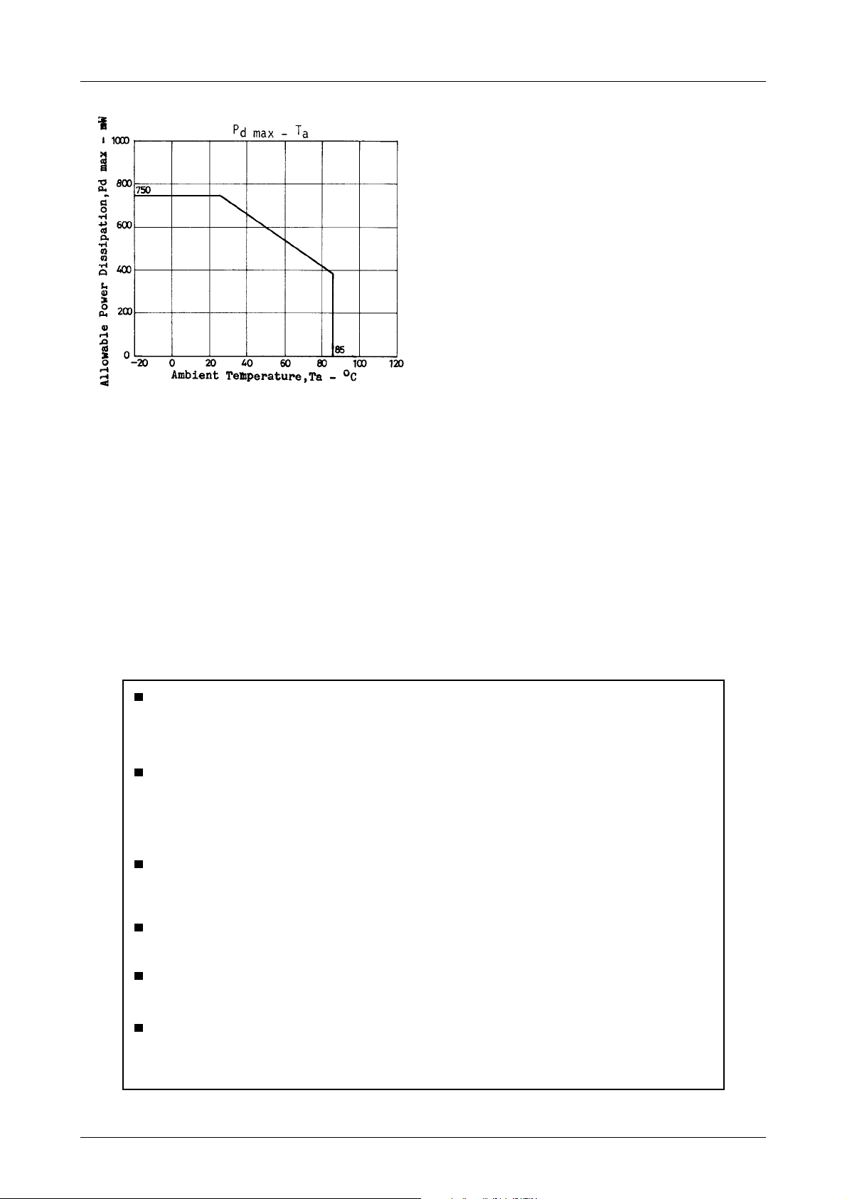
Maximum Ratings at Ta = 25˚C
retemaraPlobmySsnoitidnoCsgnitaRtinU
deilppAegatloVmumixaM
edonAdnaedohtaCssorca
tnerruCedohtaCI
tnerruCtupnIniPegatloVecnerefeRferI 01+ot50.0–Am
noitapissiDrewoPelbawollAxamdP 057Wm
erutarepmeTgnitarepOrpoT 58+ot02–
erutarepmeTegarotSgtsT 051+ot56–
V
xamedonaotdecnerefeR 73V
AK
xam 051+ot001–Am
K
Ta≤25˚C
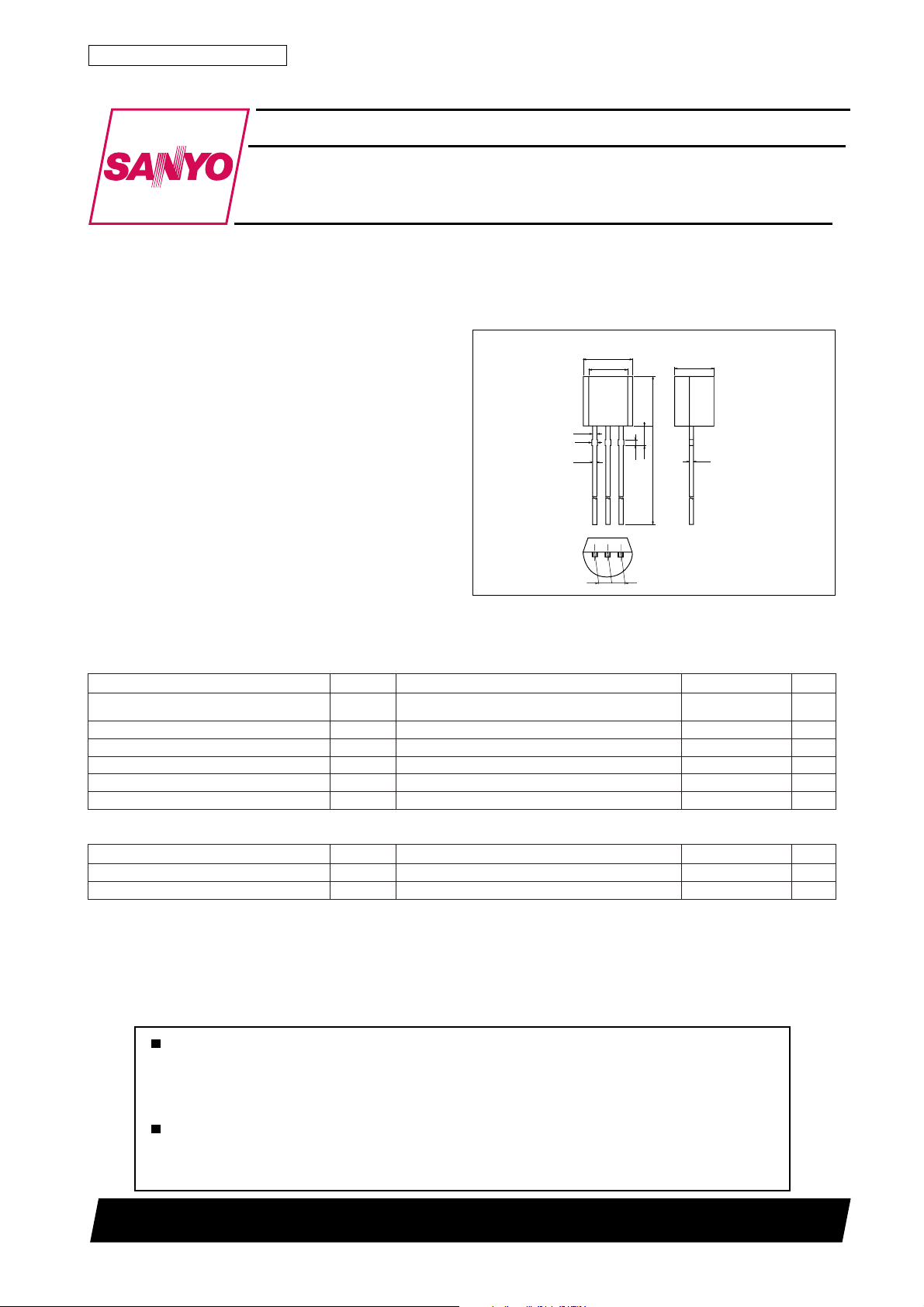
Package Dimensions
unit:mm
3101
[L5431]
1 : Reference voltage
2 : Anode
3 : Cathode
JEDEC : TO-92
EIAJ : SC-43
SANYO : NP
˚C
˚C
Recommended Operating Conditions at Ta = 25˚C
retemaraPlobmySsnoitidnoCsgnitaRtinU
edonAdnaedohtaCssorcadeilppAegatloVV
tnerruCedohtaCI
AK
K
etatsdezilibatS 001ot1Am
11200TH (KT)/O2894HK/8220TA/7237TA, TS No.2173–1/3
63otferVV
Page 2
Electrical Characteristics at Ta = 25˚C
retemaraPlobmySsnoitidnoC
egatloVecnerefeRferVVAKI,ferV=
erutarepmeThtiwegnahCegatloVecnerefeR
)1etoN(
VotoitaRegnahCferV
AK
)1etoN(erutarepmeThtiw
tnerruCedohtaCmuminiMI
tnerruCedohtaCegatS-FFOI
)2etoN(ecnatsiseRcimanyDZ|AK|VAKf,ferV= ≤ I,zHk1
∆ )aT(ferV
egnahCtnerruCtupnIniPegatloVecnerefeR
∆ )aT(ferI
Equivalent Circuit Diagram
∆ ferV
∆V
L5431
K
VKA=Vref, IK=10mA, Ta=0 to +70°C : Fig.1
I
,Am01= ∆V
K
I
AK
K
IKA=10mA, R1=10kΩ, R2=∞, Ta=0 to +70°C : Fig.2
V
NIMK
AK
V
ffoK
AK
,Am01= ∆V
AK
AK
1.giF:Am01=044259420552Vm
2.giF:ferVotV01=4.1–7.2–V/Vm
2.giF:V01otV63=0.1–0.2–V/Vm
1giF:ebaliavanoitaluger,ferV=4.01Am
3.giF:0=ferV,V63=1.01Aµ
K
sgnitaR
nimpytxam
871Vm
24Aµ
1.giF:Am001ot1=51.05.0
tinU
Ω
Input Voltage Input Voltage Input Voltage
Note1 : ∆Vref (Ta) is defined by using Vref max and Vref min as follows :
∆Vref (Ta)=Vref max – Vref min
Note2 : The dynamic resistance is defined as follows :
∆V
| ∆ZKA| =
∆I
KA
K
No.2173–2/3
Page 3
L5431
Specifications of any and all SANYO products described or contained herein stipulate the performance,
characteristics, and functions of the described products in the independent state, and are not guarantees
of the performance, characteristics, and functions of the described products as mounted in the customer's
products or equipment. To verify symptoms and states that cannot be evaluated in an independent device,
the customer should always evaluate and test devices mounted in the customer's products or equipment.
SANYO Electric Co., Ltd. strives to supply high-quality high-reliability products. However, any and all
semiconductor products fail with some probability. It is possible that these probabilistic failures could
give rise to accidents or events that could endanger human lives, that could give rise to smoke or fire,
or that could cause damage to other property. When designing equipment, adopt safety measures so
that these kinds of accidents or events cannot occur. Such measures include but are not limited to protective
circuits and error prevention circuits for safe design, redundant design, and structural design.
In the event that any or all SANYO products(including technical data,services) described or
contained herein are controlled under any of applicable local export control laws and regulations,
such products must not be exported without obtaining the export license from the authorities
concerned in accordance with the above law.
No part of this publication may be reproduced or transmitted in any form or by any means, electronic or
mechanical, including photocopying and recording, or any information storage or retrieval system,
or otherwise, without the prior written permission of SANYO Electric Co. , Ltd.
Any and all information described or contained herein are subject to change without notice due to
product/technology improvement, etc. When designing equipment, refer to the "Delivery Specification"
for the SANYO product that you intend to use.
Information (including circuit diagrams and circuit parameters) herein is for example only ; it is not
guaranteed for volume production. SANYO believes information herein is accurate and reliable, but
no guarantees are made or implied regarding its use or any infringements of intellectual property rights
or other rights of third parties.
This catalog provides information as of January, 2000. Specifications and information herein are subject
to change without notice.
PS No.2173–3/3
 Loading...