

Page 1
SANYO Electric Co.,Ltd. Semiconductor Bussiness Headquaters
TOKYO OFFICE Tokyo Bldg., 1-10, 1 Chome, Ueno, Taito-ku, TOKYO, 110-8534 JAPAN
NPN Epitaxial Planar Silicon Composite Transistor
Switching Applications
(with Bias Resistance)
Ordering number:EN3280
FC126
Features
· On-chip bias resistance (R1=47kΩ).
· Composite type with 2 transistors contained in the
CP package currently in use, improving the mounting efficiency greatly.
· The FC126 is formed with two chips, being equivalent to the 2SC3898, placed in one package.
· Excellent in thermal equilibrium and pair capability.
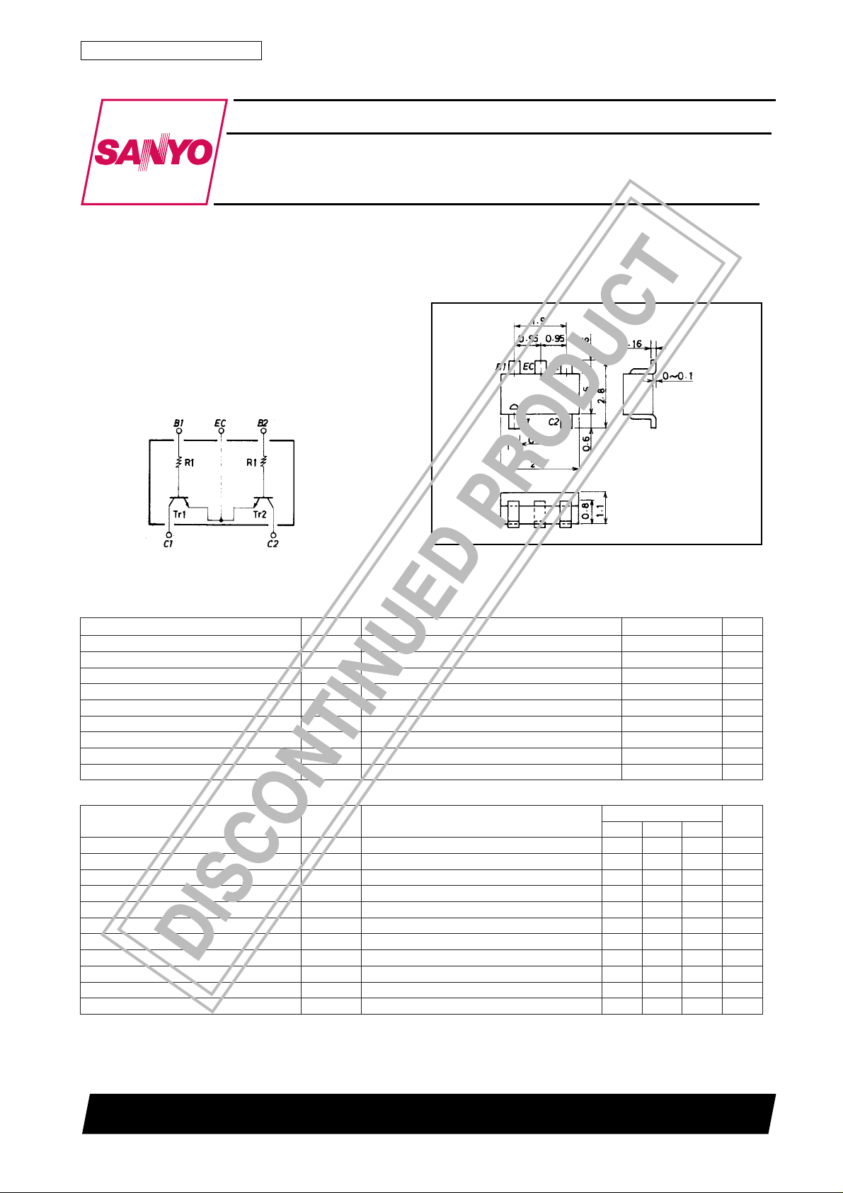
Electrical Connection
Package Dimensions
unit:mm
2066
[FC126]
C1:Collector 1
C2:Collector 2
B2:Base 2
EC:Emitter Common
B1:Base 1
Specifications
Absolute Maximum Ratings at Ta = 25˚C
retemaraPlobmySsnoitidnoCsgnitaRtinU
egatloVesaB-ot-rotcelloCV
egatloVrettimE-ot-rotcelloCV
egatloVesaB-ot-rettimEV
tnerruCrotcelloCI
tnerruCrotcelloCkaePI
noitapissiDrotcelloCP
noitapissiDrewoPlatoTP
erutarepmeTnoitcnuJjT 051
erutarepmeTegarotSgtsT 051+ot55–
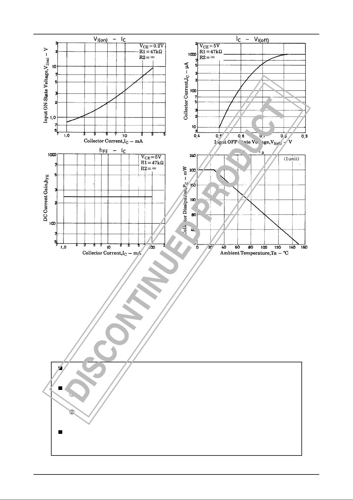
Electrical Characteristics at Ta = 25˚C
retemaraPlobmySsnotidnoC
tnerruCffotuCrotcelloCI
tnerruCffotuCrettimEI
niaGtnerruCCDh
tcudorPhtdiwdnaB-niaGf
ecnaticapaCtuptuOboCV
egatloVnoitarutaSE-CV
egatloVnwodkaerBB-CV
egatloVnwodkaerBE-CV
egatloVetatS-FFOtupnIV
egatloVetatS-NOtupnIV
ecnatsiseRtupnI1R337416kΩ
C
PC
C
T
EF
T
SANYO:CP5
sgnitaR
05V
05V
5V
001Am
002Am
003Wm
˚C
˚C
tinU
OBC
OEC
OBE
tinu1 002Wm
nimpytxam
V
OBC
V
OBE
V
V
I
)tas(EC
C
I
OBC)RB(
C
I
OEC)RB(
C
V
)ffo(I
V
)no(I
I,V04=
BC
BE
EC
EC
BC
EC
EC
0=1.0Aµ
E
I,V5=
0=1.0Aµ
C
I,V5=
Am01=001
C
I,V01=
Am5=052zHM
C
zHM1=f,V01=3.3Fp
I,Am5=
Am52.0=1.03.0V
B
I,Aµ01=
0=05V
E
R,Aµ001=
=∞ 05V
EB
I,V5=
Aµ001=4.055.08.0V
C
I,V2.0=
Am5=8.00.20.4V
C
Note:The specifications shown above are for each individual transistor.
Marking:126
52098HA (KT)/2160MO, TS No.3280-1/2
Page 2
FC126
No products described or contained herein are intended for use in surgical implants, life-support systems,
aerospace equipment, nuclear power control systems, vehicles, disaster/crime-prevention equipment and
the like, the failure of which may directly or indirectly cause injury, death or property loss.
Anyone purchasing any products described or contained herein for an above-mentioned use shall:
Accept full responsibility and indemnify and defend SANYO ELECTRIC CO., LTD., its affiliates,
subsidiaries and distributors and all their officers and employees, jointly and severally, against any
and all claims and litigation and all damages, cost and expenses associated with such use:
Not impose any responsibilty for any fault or negligence which may be cited in any such claim or
litigation on SANYO ELECTRIC CO., LTD., its affiliates, subsidiaries and distributors or any of
their officers and employees jointly or severally.
Information (including circuit diagrams and circuit parameters) herein is for example only; it is not guaranteed for volume production. SANYO believes information herein is accurate and reliable, but no guarantees
are made or implied regarding its use or any infringements of intellectual property rights or other rights of
third parties.
This catalog provides information as of May, 1998. Specifications and information herein are subject to
change without notice.
PS No.3280-2/2
 Loading...