

Page 1
Any and all SANYO products described or contained herein do not have specifications that can handle
applications that require extremely high levels of reliability, such as life-support systems, aircraft’s
control systems, or other applications whose failure can be reasonably expected to result in serious
physical and/or material damage. Consult with your SANYO representative nearest you before using
any SANYO products described or contained herein in such applications.
SANYO assumes no responsibility for equipment failures that result from using products at values that
exceed, even momentarily, rated values (such as maximum ratings, operating condition ranges,or other
parameters) listed in products specifications of any and all SANYO products described or contained
herein.
TR:NPN Epitaxial Plannar Silicon Transistor
FET:N-Channel Junction Silicon Transistor
High-Frequency Amp, AM Applications,
Low-Frequency Amp
Ordering number:ENN3482
FC12
SANYO Electric Co.,Ltd. Semiconductor Company
TOKYO OFFICE Tokyo Bldg., 1-10, 1 Chome, Ueno, Taito-ku, TOKYO, 110-8534 JAPAN
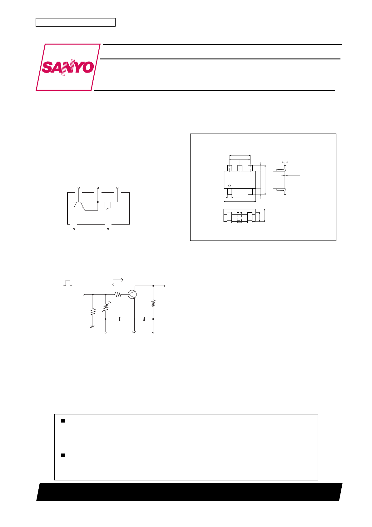
Features
· Composite type with 2 transistors contained in the
CP package currently in use, improving the mounting efficiency greatly.
· The FC12 is formed with two chips, being equivalent
to the 2SC4639, placed in one package.
· Common drain and emitter.
Electrical Connection
B S
E / D
CG
Package Dimensions
unit:mm
2075
[FC12]
1.9
0.950.95
54
3
0.60.6
1.6
2.8
1
2
0.4
2.9
1.1
0.8
0.16
0 to 0.1
C:Collector
G:Gate
S:Source
E/D:Emitter/Drain
B:Base
SANYO:CP5
Switching Time Test Circuit
I
V
R
B1
I
B2
R
B
+
220µF 470µF
+
VCC=20VVBE= --5V
OUTPUT
R
L
72301TN(KT)/52098HA (KT)/5132MH, HK No.3482-1/6
PW=20µs
D.C.≤1%
INPUT
50Ω
10IB1= --10IB2=IC=10mA
Page 2
Specifications
Absolute Maximum Ratings at Ta = 25˚C
retemaraPlobmySsnoitidnoCsgnitaRtinU
]TEF[
egatloVecruoS-ot-niarDV
egatloVniarD-ot-etaGV
tnerruCetaGI
tnerruCniarDI
noitapissiDrewoPelbawollA
]RT[
egatloVesaB-ot-rotcelloCV
egatloVrettimE-ot-rotcelloCV
egatloVesaB-ot-rettimEV
tnerruCrotcelloCI
)esluP(tnerruCrotcelloCI
tnerruCesaBI
noitapissiDrotcelloCP
]sgnitaRnommoC[
noitapissiDlatoTTP 003Wm
erutarepmeTnoitcnuJjT 051
erutarepmeTegarotSgtsT 051+ot55–
Marking:12
G
D
P
D
C
B
C
FC12
XSD
SDG
OBC
OEC
OBE
PC
51V
51–V
01Am
05Am
002Wm
55V
05V
6V
051Am
003Am
03Am
002Wm
˚C
˚C
Electrical Characterisitics at Ta = 25˚C
retemaraPlobmySsnoitidnoC
]TEF[
egatloVnwodkaerBniarD-ot-etaGV
tnerruCffotuC-ot-etaGI
egatloVffotuCV
tnerruCniarDI
ecnattimdArefsnarTdrawroFY|sf|VSDV,V5=
ecnaticapaCtupnIssiCVSDV,V5=
ecnaticapaCrefsnarTesreveRssrCVSDV,V5=
erugiFesioNFNVSDk1=gR,V5= ,Ω I
]RT[
tnerruCffottuCrotcelloCI
tnerruCffotuCrettimEI
niaGtnerruCCDh
tcudorPhtdiwdnaB-niaGf
ecnaticapaCtuptuOboCV
egatloVnoitarutaSE-CV
egatloVnoitarutaSE-BV
egatloVnwodkaerBB-CV
egatloVnwodkaerBE-CV
egatloVnwodkaerBB-EV
emiTNO-nruTt
emiTegarotSt
emiTllaFt
Note*:The FC12 is classified by I
0.21F0.60.02G0.01
as follows : (unit:mA).
DSS
I
SDG)RB(
G
V
SSG
V
)ffo(SG
V
SSD
V
OBC
V
OBE
V
EF
V
T
I
)tas(EC
C
I
)tas(EB
C
I
OBC)RB(
C
I
OEC)RB(
C
I
OBE)RB(
E
no
gts
f
V,Aµ01–=
0=51–V
SD
V,V01–=
SG
SD
SD
BC
BE
EC
EC
BC
0=0.1–An
SD
I,V5=
Aµ001=2.0–6.0–4.1–V
D
V,V5=
0=*0.6*0.02Am
SG
SG
SG
SG
I,V53=
0=1.0Aµ
E
I,V4=
0=1.0Aµ
C
I,V6=
C
I,V6=
C
I,Am05=
B
I,Am05=
B
I,Aµ01=
0=55V
E
R,Am1=
=∞ 05V
EB
I,Aµ01=
0=6V
C
zHk1=f,0=5205Sm
zHM1=f,0=01Fp
zHM1=f,0=0.3Fp
D
Am1=531004
Am01=002zHM
zHM1=f,V6=7.1Fp
Am5=80.04.0V
Am5=8.00.1V
tiucriCtseTdeificepseeS51.0sµ
tiucriCtseTdeificepseeS57.0sµ
tiucriCtseTdeificepseeS02.0sµ
sgnitaR
nimpytxam
zHk1=f,Am1=5.1Bd
tinU
No.3482-2/6
Page 3

Primany Characteristics of FET
16
14
12
-- mA
10
D
8
6
4
Drain Current, I
2
0
0 0.4 0.8 1.2 1.6 2.0
ID -- V
Drain-to-Source Voltage, VDS -- V
ID -- V
DS
GS
--0.6V
=0
V
GS
--0.1V
--0.2V
--0.3V
--0.4V
--0.5V
VDS=5V
FC12
40
20
16
-- mA
12
D
ID -- V
DS
=0
V
GS
--0.1V
8
--0.2V
Drain Current, I
4
--0.3V
--0.4V
0
0246810
--0.6V
--0.5V
Drain-to-Source Voltage, VDS -- V
2
VGS(off) -- I
DSS
VDS=5V
ID=100µA
=20mA
I
DSS
--1.2 --1.0 --0.8 --0.6 --0.4 --0.2 0
Gate-to-Source Voltage, VGS -- V
Forward Transfer Admittance, yfs -- mS
100
yfs -- I
7
5
3
2
10
7
5
3
1.0
3
2
=6mA
I
DSS
Drain Current, I
Ciss -- V
10m
A
10
D
DS
D
20mA
-- mA
15mA
10mA
6mA
VDS=5V
f=1kHz
VGS=0
f=1MHz
30
20
10
0
5327532
--1 .0
-- V
-- mA
D
Drain Current, I
(off)
GS
Cutoff Voltage, V
Forward Transfer Admittance, yfs -- mS
7
5
3
2
--0 .1
100
7
5
3
2
10
10
7
57 2 335
10
Drain Current, I
yfs -- I
DSS
DSS
-- mA
VDS=5V
VGS=0
f=1kHz
10
Drain Current, I
Crss -- V
DSS
-- mA
DS
533275
VGS=0
f=1MHz
Input Capacitance, Ciss -- pF
1.0
5
10
Reverse Transfer Capacitance, Crss -- pF
1.0
3
2
7
5
1.0
23 577
Drain-to-Source V oltage, V
DS
10
235
-- V
7
5
3
2
1.0
23 35577
Drain-to-Source V oltage, V
10
DS
2
-- V
No.3482-3/6
Page 4

FC12
14
12
NF -- f
VDS=5V
ID=10mA
14
12
NF -- f
VDS=5V
Rg=1kΩ
10
8
Rg=500
6
4
Noise Figure, NF -- dB
10k
2
Ω
0
10 100 1k
250
200
Ω
1k
Ω
51M25225
Frequency, f -- Hz
P
D
-- mW
D
150
100
50
Collector Dissipation, P
0
0 20 40 60 80 100 120 140 160
Ambient Temperature, Ta -- °C
Primany Characteristic of TR
I
450µA
I
C
C
50
40
500µA
-- mA
C
30
20
Collector Current, I
10
0
0 0.4 1.00.80.60.2
Collector-to-Emitter Voltage, V
160
140
120
-- mA
C
100
80
60
40
Collector Current, I
20
0
0 0.2 0.4 0.80.6 1.0 1.41.2
Base-to-Emitter V oltage, V
-- V
-- V
°C
Ta=75
-- Ta
CE
400
BE
25°C
10k
µA
--25°C
25
350µA
300
250µA
200µA
150µA
100µA
IB=0
CE
-- V
BE
100k
µA
50µA
-- V
VCE=6V
25
10
I
D
=1mA
8
6
3mA
4
Noise Figure, NF -- dB
10mA
2
0
51M25225
10 100 1k
12
10
50µA
Frequency, f -- Hz
45µA
-- mA
8
C
6
4
Collector Current, I
2
0
020 504010 30
Collector-to-Emitter Voltage, V
2
1000
7
FE
5
3
2
100
DC Current Gain, h
7
5
3
325
0.1
Ta=75
1.0
Collector Current, I
25
10k
I
-- V
C
CE
40µA
35µA
30µA
25µA
20µA
CE
h
-- I
FE
C
°C
25°C
--25°C
32325
10
-- mA
C
25
100k
15µA
10µA
5µA
IB=0
-- V
VCE=6V
100
No.3482-4/6
325
Page 5

7
5
3
-- MHz
T
2
100
7
5
Gain Bandwidth product, f
3
2
1.0 10
52732
Collector Current, I
3
2
-- pF
10
7
5
3
2
1.0
Gain Bandwidth Product, Cob
7
5
1.0 10
Cob -- V
Collector-to-Base Voltage, V
VBE(sat) -- I
(sat) -- V
10
BE
7
5
3
2
FC12
f
T
5757 32
-- I
C
CB
C
-- mA
CB
C
VCE=6V f=1MHz
5
3
2
-- pF
ib
10
7
5
3
Input Capacitance, c
2
1.0
5732
100
57 5732
Emitter-to-Base Voltage, V
f=1MHz
5732
100
3
2
1.0
7
(sat) -- V
5
CE
3
2
0.1
7
5
Collector-to-Emitter
Saturation V oltage, V
3
2
1.0
-- V
IC / IB=10
250
200
-- mW
C
150
c
-- V
ib
1.0 10
VCE(sat) -- I
EB
EB
C
-- V
IC / IB=10
°C
Ta=75
--25
723 5 72235
10 100
Collector Current, I
P
-- Ta
C
C
°C
25°C
-- mA
1.0
7
5
Base-to-Emittter
Saturation V oltage, V
3
1.0
°C
Ta= --25
°C
75
723 5 72235
10 100
Collector Current, I
25°C
C
-- mA
100
50
Collector Dissipation, P
0
2006040 80 100 140120 160
Ambient Temperature, Ta -- °C
No.3482-5/6
Page 6

FC12
Specifications of any and all SANYO products described or contained herein stipulate the performance,
characteristics, and functions of the described products in the independent state, and are not guarantees
of the performance, characteristics, and functions of the described products as mounted in the customer's
products or equipment. To verify symptoms and states that cannot be evaluated in an independent device,
the customer should always evaluate and test devices mounted in the customer's products or equipment.
SANYO Electric Co., Ltd. strives to supply high-quality high-reliability products. However, any and all
semiconductor products fail with some probability. It is possible that these probabilistic failures could
give rise to accidents or events that could endanger human lives, that could give rise to smoke or fire,
or that could cause damage to other property. When designing equipment, adopt safety measures so
that these kinds of accidents or events cannot occur. Such measures include but are not limited to protective
circuits and error prevention circuits for safe design, redundant design, and structural design.
In the event that any or all SANYO products(including technical data,services) described or
contained herein are controlled under any of applicable local export control laws and regulations,
such products must not be exported without obtaining the export license from the authorities
concerned in accordance with the above law.
No part of this publication may be reproduced or transmitted in any form or by any means, electronic or
mechanical, including photocopying and recording, or any information storage or retrieval system,
or otherwise, without the prior written permission of SANYO Electric Co. , Ltd.
Any and all information described or contained herein are subject to change without notice due to
product/technology improvement, etc. When designing equipment, refer to the "Delivery Specification"
for the SANYO product that you intend to use.
Information (including circuit diagrams and circuit parameters) herein is for example only ; it is not
guaranteed for volume production. SANYO believes information herein is accurate and reliable, but
no guarantees are made or implied regarding its use or any infringements of intellectual property rights
or other rights of third parties.
This catalog provides information as of July, 2001. Specifications and information herein are subject to
change without notice.
PS No.3482-6/6
 Loading...