

Samsung X700 Service Manual
GSM TELEPHONE
SGH-X700
GSM TELEPHONE
CONTENTS
1. Specification
2. Circuit Description
3. Exploded Views and Parts List
4. Electrical Parts List
5. Block Diagrams
6. PCB Diagrams
7. Flow Chart of Troubleshooting

1. Specification
1-1. GSM General Specification
GSM900
Phase 1
Freq. Band[MHz]
Uplink/Downlink
ARFCN range 1~124
Tx/Rx spacing 45MHz 45MHz 95MHz
Mod. Bit rate
/BitPeriod
Time Slot Period
/ Frame Period
Modulation 0.3GMSK 0.3GMSK 0.3GMSK
MS Power 33dBm~5dBm 33dBm~5dBm 30dBm~0dBm
890~915
935~960
270.833kbps
3.692us
576.9us
4.615ms
EGSM 900
Phase 2
880~915
925~960
0~124 &
975~1023
270.833kbps
3.692us
576.9us
4.615ms
DCS1800
Phase 1
1710~1785
1805~1880
512~885
270.833kbps
3.692us
576.9us
4.615ms
PCS1900
1850~1910
1930~1990
512~810
80MHz
270.833kbps
3.692us
576.9us
4.615ms
0.3GMSK
30dBm~0dBm
Power Class 5pcl ~ 19pcl 5pcl ~ 19pcl 0pcl ~ 15pcl
Sensitivity -102dBm -102dBm -100dBm
TDMA Mux 8 8 8
Cell Radius 35Km 35Km 2Km
0pcl ~ 15pcl
-100dBm
8
-
1-1
SAMSUNG Proprietary-Contents may change without notice
This Document can not be used without Samsung's authorization

Specification
1-2. GSM TX power class
TX Power
control level
5 33±3 dBm
6 31±3 dBm
7 29±3 dBm
8 27±3 dBm
9 25±3 dBm
10 23±3 dBm
11 21±3 dBm
GSM900
TX Power
control level
0 30±3 dBm
1 28±3 dBm
2 26±3 dBm
3 24±3 dBm
4 22±3 dBm
5 20±3 dBm
6 18±3 dBm
DCS1800
TX Power
control level
0 30±3 dBm
1 28±3 dBm
2 26±3 dBm
3 24±3 dBm
4 22±3 dBm
5 20±3 dBm
6 18±3 dBm
PCS1900
12 19±3 dBm
13 17±3 dBm
14 15±3 dBm
15 13±3 dBm
16 11±5 dBm
17 9±5 dBm
18 7±5 dBm
19 5±5 dBm
7 16±3 dBm
8 14±3 dBm
9 12±4 dBm
10 10±4 dBm
11 8±4dBm
12 6±4 dBm
13 4±4 dBm
14 2±5 dBm
7 16±3 dBm
8 14±3 dBm
9 12±4 dBm
10 10±4 dBm
11 8±4dBm
12 6±4 dBm
13 4±4 dBm
14 2±5 dBm
15 0±5 dBm
1-2
15 0±5 dBm
SAMSUNG Proprietary-Contents may change without notice
This Document can not be used without Samsung's authorization
2. Circuit Description
2-1. SGH-X700 RF Circuit Description
2-1-1. RX PART
- FRONT END MODULE(ANTENNA SWITCH MODULE + RX SAW FILTER) (U100)
It performs to switch Tx & Rx paths for GSM900, DCS1800 and PCS1900 with logic controls below.
- FEM Control Logic Table
FESW1 FESW2
Tx Mode (GSM900) H L
Tx Mode (DCS1800/1900) L H
Rx Mode (GSM900) L L
Rx Mode (DCS1800) L L
Rx Mode (PCS1900) L L
- VC-TCXO (TCX100)
This module generates the 26MHz reference clock to drive the logic and RF systems.
It is turned on when the supply voltage (+VCC_SYN_2V8) is applied.
After buffering, the 26MHz reference clock is supplied to the other parts of the system through the transceiver pin
CLKOUT.
- Transceiver (U102)
This chip is fully integrated GSM & GPRS tri-band transceiver with RF VCO, loop filters and most of the
passive components required in it.
It also fully integrated fractional N RF synthesizer with AFC control possibility, RF VCO with integrated supply
regulator. Semi integrated reference oscillator with integrated supply regulator.
RF Receiver front-end amplifies the E-GSM900, DCS1800 and PCS1900 aerial signal, convert the chosen channel
down to a low IF of 100kHz.
In IF section, further amplifies the wanted channel, performs gain control to tune the output level to the desired value and
rejects DC.
2-1-2. TX PART
The transmitter is fully differential using a direct up conversion architecture. It consists of a signal side band
power up mixer. Gain is controlled by 6 dB via 3-wire serial bus programing. The fully integrated VCO and power
mixer achieve LO suppression, quadrature phase error, quadrature amplitude balance and low noise floor specification.
Output matching/balun components drive a standard 50 ohms single ended load.
2-1
SAMSUNG Proprietary-Contents may change without notice
This Document can not be used without Samsung's authorization

Circuit Description
2-2. Baseband Circuit description of SGH-X700
2-2-1. PCF50603 (U400)
- Power Management
Eight low-dropout regulators designed specifically for GSM applications power the terminal and help ensure optimal
system performance and long battery life. A programmable boost converter provides support for 1.8V, 3.0V SIMs,
while a self-resetting, electronically fused switch supplies power to external accessories. Ancillary support functions,
such as RTC module and High Voltage Charge pump, Clock generator, aid in reducing both board area and system
complexity.
I2C BUS serial interface provides access to control and configuration registers. This interface gives a microprocessor
full control of the PCF50603 and enables system designers to maximize both standby and talk times.
Supervisory functions. including a reset generator, an input voltage monitor, and a temperature sensor, support reliable
system design. These functions work together to ensure proper system behavior during start-up or in the event of a
fault condition(low microprocessor voltage, insufficient battery energy, or excessive die temperature).
- Pulse-Width Modulator
The Backlight Brightness Modulator (BBM) contains a programmable Pulse-width modulator (PWM) to modulate the
intensity of a series of LED's or to control a DC/DC converter that drives LCD backlight.
This phone is using PWM control to modulate the LCD backlight brightness.
- Clock Generator
The Clock Generator (CG) generates all clocks for internal and external usage. The 32.768 kHz crystal oscillator
provides an accurate low clock frequency for the PCF50603 and other circuitry.
2-2-2. LCD
X700 has just one 1.9" TFT LCD. 16-bit data lines(LD(0)~LD(15)) transfers data and commands to LCD. There are
couple of control signals such as RS, CS, RD, WR, etc. RS stands for "Register Select pin." When RS = 0, data can be
written to the index register or status can be read, and when RS = 1, an instruction can be issued or data can be written
to or read from RAM. Read or write operation is selected according to RD/WR signals. The data is received when the
R/W bit is 0, and is transmitted when the R/W bit is 1.
At the falling edge of CS input, serial data transfer is
initiated. On the other hand, at the rising edge of CS input, the data transfer is ceased.
2-2-3. Key
Key recognition part is consisted of 8 ports from PCF5213EL1. KEY_ROW(0:4) & KEY_COL(0:4)
These signals performs with the matrix. Any input from the matrix informs the key status to key interface in the
PCF5213EL1. Power on/off key is independent of the matrix. Therefore, 'power on/off' signal is directly connected with
PCF50603 to turn PCF50603 on.
3.3V LDO(U700) enables Key LED on. Key LED consists of 12 LEDs. It is controlled by "Key_led_on" signal.
2-2
SAMSUNG Proprietary-Contents may change without notice
This Document can not be used without Samsung's authorization

Circuit Description
2-2-4. EMI ESD Filter (U500)
This system uses the EMI ESD filter (U500) to protect the device from noises from IF CONNECTOR part.
2-2-5. IF connetor (IFC500)
It has 18-pin. They are designed to allocate VBAT, V_EXT_CHARGE, USB_D+, +VBUS, USB_D-, TXD1, RXD1,
AUX_ON, EXT1, EXT2 and GND. They connected to power supply IC, microprocessor and signal processor IC.
2-2-6. Battery Charge Management
X700 has a complete constant-current/constant-voltage linear charger for single cell lithium-ion batteries inside.
If Travel Adapter is connected, "V_EXT_CHARGE" begins to provide the charger IC (to battery) with power (current).
When the charging operation is done, "End_of_charge" informs it to PCF5213EL1 to stop the operation. "CHG_ON"
signal enables the charger IC to operate in adequate circumstances.
2-2-7. Audio - Part
X700 has several audio-outputs such as stere speaker, receiver, earphone, etc. RCV_P/N signals from CPU are connected
to the receiver via analog switche (U602). MIC_P/N are connected to the main MIC as well.
YMU762 is a synthesizer LSI for mobile phones. This LSI has a built-in speaker amplifier for outputting sounds that are
used by mobile phones in addition to game sounds and ringing melodies that are replayed by a synthesizer.
YMU762 has built a speaker amplifier of which maximum out is 580 mW at SPVDD=3.6V in this device. There is
Stereophonic analog output for Headphone.
2-2-8. Memory (UME300)
X700 has
The
Flash Memory and 512Mbit OneNAND Flash and 128Mbit Synchronous Burst U tRAM.
It has 16 bit data line, HD[1~16] which is connected to PCF5213 and MV3315DOQ, also has 24 bit address lines,
HA[1~24]. There are 3 chip select signals, CS0n_FLASH, CS1n_RAM, and CS4n_NAND.
Inthewrtingprocess,WEnisfallentolowanditenableswriting process to operate. During reading process,
OEn is fallen to low and it enables reading process to operate. Each chip select signals in the PCF5213EL1 choose
different types of memory.
KAP17SG00A-D4U4
KAP17SG00A-D4U4
as a memory module.
is a Multi Chip Package Memory which combines 256Mbit Synchronous Burst Multi Bank NOR
2-2-9. PCF5213EL1 (UCP200)
The PCF5213EL1 is mainly composed of embeded DSP and ARM core. The DSP subsystem includes the Saturn
DSP core with embedded RAM and ROM, and a set of peripherals. It has 24k×16 bits PRAM, 104k×16 bits,
32k×16 XYRAM and 63k×16 XYROM in the DSP.
The ARM946E-S consists of an ARM9E-S processor core, 8 kbyte instruction cache and 8 kbyte data cache,
tightly-coupled ITCM (Instruction Tightly Coupled Memory) and DTCM (Data Tightly Coupled Memory) memories, a
memory protection unit, and an AMBA (Advanced Microcontroller Bus Architecture) AHB (Advanced
High-performance Bus) bus interface with a write buffer.
HD(0:15), data lines and HA(0:23), address lines are connected to KAP17SG00A (memory), MV3018B (image dsp)
and YMU762 (melody IC). It has 64 kbyte SC RAM (0.5 Mbit) and 32 kbyte SC program ROM for bootstrap
loader in the ARM core.
2-3
SAMSUNG Proprietary-Contents may change without notice
This Document can not be used without Samsung's authorization

Circuit Description
HD(0:15), data lines and HA(0:23), address lines are connected to memory and YMU762 to communicate.
MV3018B(Camera DSP Chip) controls the communication between ARM core and DSP core.
OEn, WEn control the access of memory. KROW, and KCOL recognize the key string input status.
It has J-TAG control pins (TDI/TDO/TCK) for ARM and DSP core. J-SEL signal controls different access to ARM
and DSP core.
ADC(Analog to Digital Convertor) receives the condition of temperature, battery type and battery voltage.
HD(0:15), data lines and HA(0:23), address lines are connected to memory and YMU762 to communicate.
MV3315DOQ(Camera DSP Chip) controls the communication between ARM core and DSP core.
OEn, WEn control the access of memory. KROW, and KCOL recognize the key string input status.
It has J-TAG control pins (TDI/TDO/TCK) for ARM and DSP core. J-SEL signal controls different access to ARM
and DSP core.
ADC(Analog to Digital Convertor) receives the condition of temperature, battery type and battery voltage.
2-2-10. VC-TCXO-214C6 (TCX100, 26MHz)
This system has the 26MHz TCXO, TCO-5871U from Toyocom. AFC controlling signal form PCF5213EL1 controls
frequency from 26MHz X-tal. It generates the clock frequency. This clock is connected to PCF5213EL1, YMU762 and
UAA3587.
2-2-11. Camera DSP (U303, MV3315DOQ)
MV3315DOQ provides rich video functions up to 30-frame display with minimized tasks in the handset main processor
as well as hardware based real-time JPEG compression and decompression. MV3315DOQ directly transmits and
previews the RGB data to the LCD graphic memory by processing the sensor output data according to the
handset's command. It can save the raw RGB data up to VGA resoultion into its image buffer and allows the
host processor to download with scalable sized compressed data.
It utilizes 16 bit data bus for communication with the main processor, including bus interface types.
2-4
SAMSUNG Proprietary-Contents may change without notice
This Document can not be used without Samsung's authorization

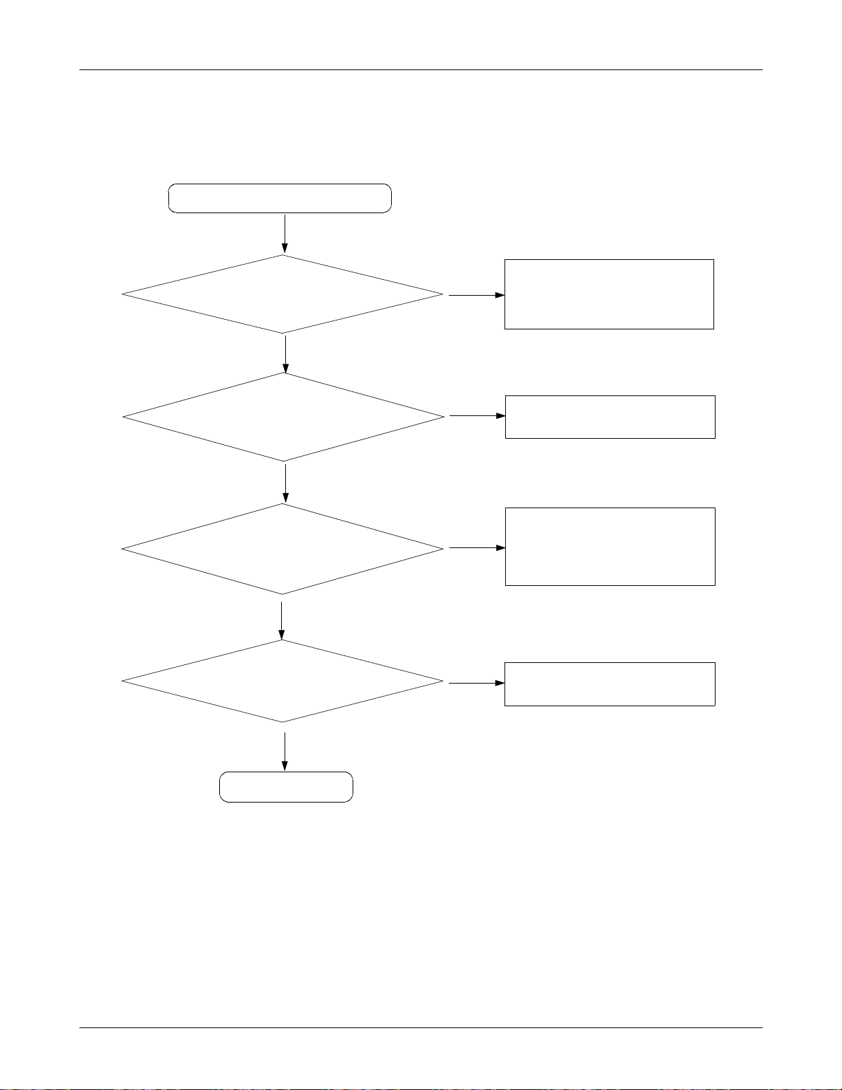
7. Flow Chart of Troubleshooting
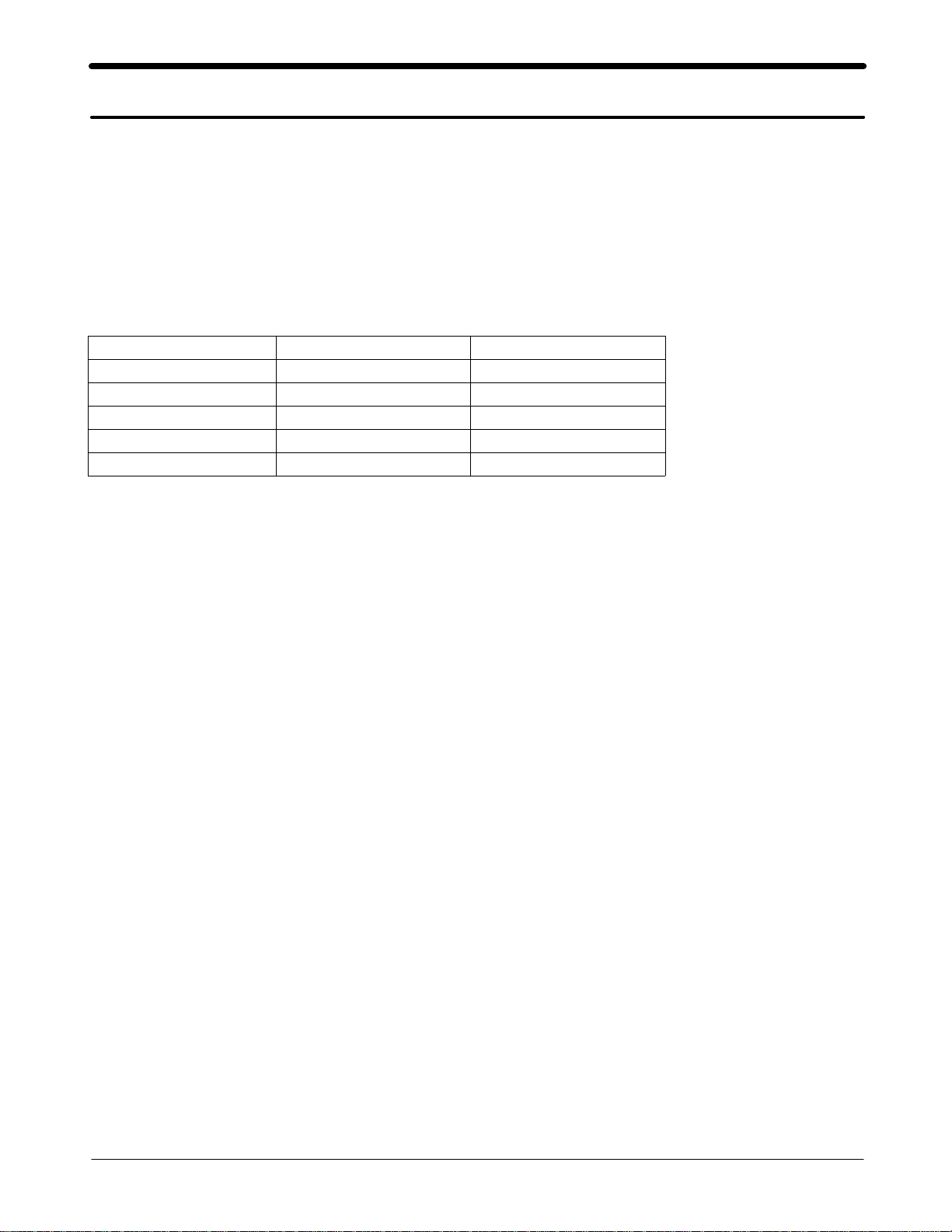
7-1. Power On
' Power On ' does not work
Yes
Check the Battery Voltage
is more than 3.4V
Yes
C408(VINT) = 2.7V?
Yes
Check the Clock at
R401=32KHZ
Yes
C427(+VDD_IO_LOW) &
C426(+VDD_IO_HIGH) = "H"?
Yes
No
Charge the Battery
No
Check the PMU related to VINT
No
Resolder OSC400
No
Check the related circuit
C404(+VDD_GSM_CORE)
= 1.875V?
Yes
Check for the clock at C124
= 26MHz
Yes
Check the initial operation
Yes
END
SAMSUNG Proprietary-Contents may change without notice
This Document can not be used without Samsung's authorization
No
No
7-1
Check the +VDD_GSM_CORE circuit
Check the clock generation circuit
(related to TCX100)
Flow Chart of Troubleshooting
ONKEYN
+VDD_RX_TX_2V8
+VCC_SYN_2V8
+VDD_BT_1V8
+VDD_CAM_2V8
+VDD_IO_HIGH_2V9
+VDD_IO_LOW_1V8
C409
C411
VBAT
V400
C413
L402
C415
C416
C417
C424
C426
C427
OSC400
R401
C412
C407
C408
R404
2341
27
29
25
28
26
I
Y
T
C
O
C
E
F
N
C
I
S
K
E
S
V
O
N
R
O
O
_
24
RF2VDD
23
RF12VBAT
22
RF1VDD
21
D1VDD
20
LPD1VBAT
19
LPVDD
18
HCVBAT
17
HCVDD
16
D2VDD
15
IOD2VBAT
14
IOVDD
13
_REC2
S
C
A
H
I
T
B
Q
S
C
I
R
R
I
_
_
M
12
11
10
C425
BAT400
RB414II06N
LCD_BL_ON
C414
R402
R403
BACKLIGHT
T400
32
30
33
36
35
31
34
X
T
V
T
E
D
G
A
V
A
S
V
C
H
O
I
M
I
S
9
A
R
A
D
H
D
B
C
V
G
V
H
C
U400
C
C
1
2
H
H
S
N
N
K
R
E
E
C
R
R
M
I
M
W
W
I
S
_
S
P
P
8
7
6
37
M
B
V
SCP
T
V
P
A
P
C
B
C
/
38
SCN
R
U
C
39
G
D3VDD
H
C
40
SIMD3VBAT
41
SIMVCC
42
SIMIOCD
43
SIMCKCD
44
_SIMRSCD
45
SIMEN
46
GPO3
47
GPO2
48
GPO1
49
GND
50
GND
51
GND
52
K
GND
1
2
3
53
C
NC
L
A
K
E
54
L
C
D
R
NC
_
S
S
C
2
3
1
5
4
C418
+VDD_SD_2V9
+VDD_IO_LOW_1V8
C419
C420
SIM_VCC
SIM_IO
SIM400
SIM_CLK
SIM_RST
C421
6
1
6
1
5
22
5
4
33 4
G
G
G78G
910
C423
AUX_ON
SCL
SDA
32KHz_DIGIT
PON_TX
REF_ON
SIMRST
SIMCLK
MIC_BIAS_2V1
RSTON
IT_PMU
SIMIO
7-2
SAMSUNG Proprietary-Contents may change without notice
This Document can not be used without Samsung's authorization

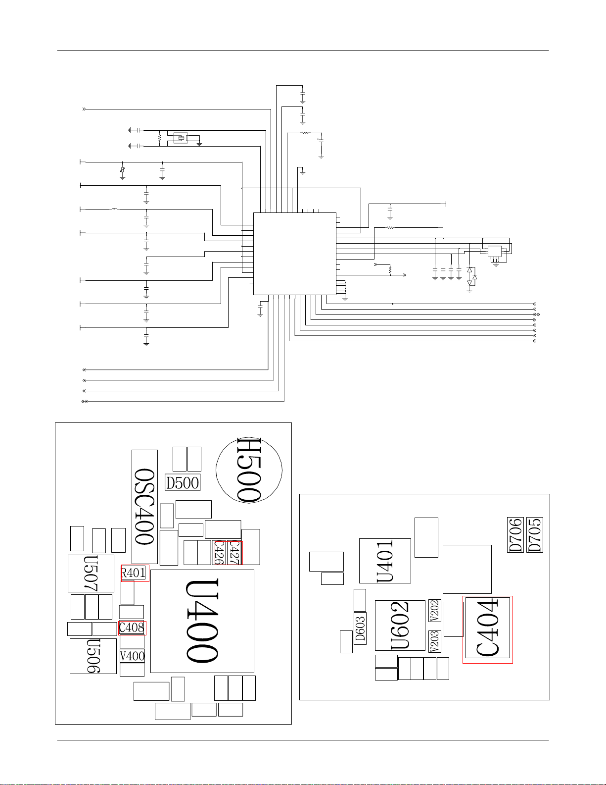
7-2. Initial
Flow Chart of Troubleshooting
Initial Failure
Yes
TP231 (RSTON) ="H"?
Yes
Is U308 pin 4
OK?
Yes
Check the 16bit data signal
&memoryCE
Yes
END
No
Check the circuit related to reset
No
Check the U308
7-3
SAMSUNG Proprietary-Contents may change without notice
This Document can not be used without Samsung's authorization

Flow Chart of Troubleshooting
HA(25)
+VDD_IO_LOW_1V8
GND
OUT
3
IN
2
NC
VCC
1
U308
R300
+VDD_IO_LOW_1V8
+VDD_IO_LOW_1V8
4
5
R317
C304C303 C336
HA(1:16)
HA(1:24)
OEn
CS0n_FLASH
OEn
WEn
CS4n_NAND
BE1n
HA(0)
WEn
CLKBURST
RSTEXTn
CS1n_RAM
ADVn
RSTEXTn
HA(1)
HA(2)
HA(3)
HA(4)
HA(5)
HA(6)
HA(7)
HA(8)
HA(9)
HA(10)
HA(11)
HA(12)
HA(13)
HA(14)
HA(15)
HA(16)
HA(1)
HA(2)
HA(3)
HA(4)
HA(5)
HA(6)
HA(7)
HA(8)
HA(9)
HA(10)
HA(11)
HA(12)
HA(13)
HA(14)
HA(15)
HA(16)
HA(17)
HA(18)
HA(19)
HA(20)
HA(21)
HA(22)
HA(23)
HA(24)
R314
TP315
100K
TP308
B11
N11
N10
P11
N12
G12
F10
E11
G10
F11
K11
K10
L11
L10
D10
E10
D11
C10
C11
D12
H11
G11
H10
P12
J11
J10
B3
B7
P7
N3
P5
P6
B5
N1
N5
N6
N9
F3
L2
F9
G8
G9
H9
K9
K8
K6
C2
D2
E2
C3
D3
E3
C4
F8
C9
D9
E9
G7
B4
D4
E8
D8
D6
P3
N4
M4
L4
E4
C1
C6
C7
B8
B9
E5
D7
G6
E7
C5
J9
N8
P1
P2
P9
1
2
VCCU
VCCU
VCCU
VCCU
VCCU
VCCU
VCCQU
VCCQU
VCCQU
VCCQU
VCCR
VCCR
VCCR
VCCQR
VCCQR
VCCQR
VCCO
VCCO
VCCO
A0O
A1O
A2O
A3O
A4O
A5O
A6O
A7O
A8O
A9O
A10O
A11O
A12O
A13O
A14O
A15O
A0RU
A1RU
A2RU
A3RU
A4RU
A5RU
A6RU
A7RU
A8RU
A9RU
A10RU
A11RU
A12RU
A13RU
A14RU
A15RU
A16RU
A17RU
A18RU
A19RU
A20RU
A21RU
A22RU
A23R
/OEU
/OER
/CER
/OEO
/WEO
/CEO
/WPR
/UBU
/LBU
/WER
/WEU
CLKO
/RESETR
_CSU
INTO
AVDO
_MRSU
VPPR
_RESETO
NC
NC
NC
NC
NC
NC
NC
UME300
VSS
VSS
VSS
VSS
VSS
VSS
VSS
VSS
VSS
VSS
VSS
VSS
DQ0O
DQ1O
DQ2O
DQ3O
DQ4O
DQ5O
DQ6O
DQ7O
DQ8O
DQ9O
DQ10O
DQ11O
DQ12O
DQ13O
DQ14O
DQ15O
DQ0RU
DQ1RU
DQ2RU
DQ3RU
DQ4RU
DQ5RU
DQ6RU
DQ7RU
DQ8RU
DQ9RU
DQ10RU
DQ11RU
DQ12RU
DQ13RU
DQ14RU
DQ15RU
DNU
DNU
DNU
DNU
DNU
DNU
DNU
DNU
DNU
DNU
DNU
CLKRU
RDYR_WAITU
RDYO
_AVDRU
B2
B10
C8
E12
F2
J12
K2
M2
N2
P4
P8
P10
M3
L5
K5
J4
J3
H4
G3
G5
K4
L3
K3
J5
H3
H5
G4
F4
M5
L6
M6
N7
K7
M8
L9
M10
J7
J8
M7
L7
L8
H8
M9
M11
A2
A3
A10
A11
A12
R1
R2
R3
R10
R11
R12
E6
D5
F5
F6
B1
NC
B6
NC
B12
NC
C12
NC
D1
NC
E1
NC
F1
NC
F7
NC
F12
NC
G1
NC
G2
NC
H1
NC
H2
NC
H12
NC
H6
NC
H7
NC
J1
NC
J2
NC
J6
NC
K12
NC
K1
NC
L1
NC
L12
NC
M1
NC
M12
NC
HD(0)
HD(1)
HD(2)
HD(3)
HD(4)
HD(5)
HD(6)
HD(7)
HD(8)
HD(9)
HD(10)
HD(11)
HD(12)
HD(13)
HD(14)
HD(15)
HD(0)
HD(1)
HD(2)
HD(3)
HD(4)
HD(5)
HD(6)
HD(7)
HD(8)
HD(9)
HD(10)
HD(11)
HD(12)
HD(13)
HD(14)
HD(15)
TP316
TP307
R312
MEMORY
HD(0:15)
HD(0:15)
CLKBURST
WAITn
ADVn
+VDD_IO_LOW_1V8
7-4
SAMSUNG Proprietary-Contents may change without notice
This Document can not be used without Samsung's authorization
Flow Chart of Troubleshooting
7-5
SAMSUNG Proprietary-Contents may change without notice
This Document can not be used without Samsung's authorization
Flow Chart of Troubleshooting
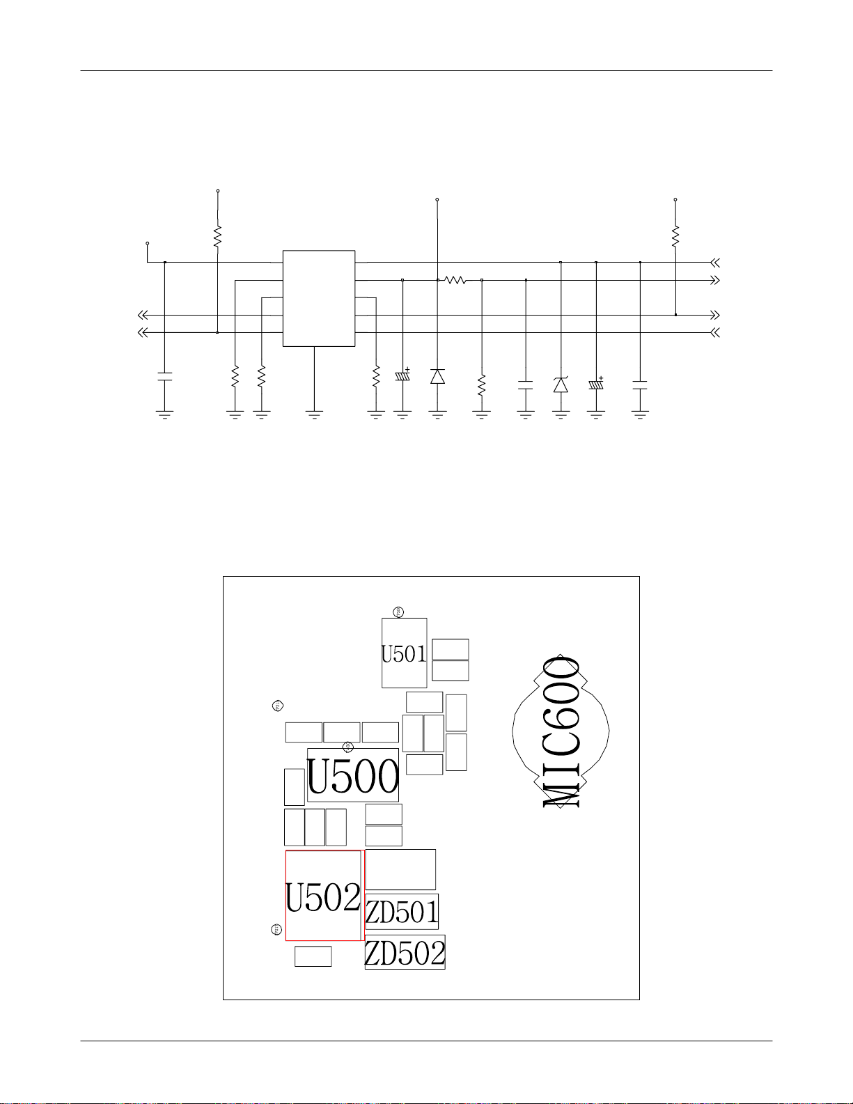
7-3. Charging Part
Abnormal charging part
Yes
Check the U502 pin 10
>4.9V
Yes
U502 pin 6 = "L"?
Yes
U502 pin 4 = "L"?
Yes
Check the U502 pin 9
≒4.2V
No
No
No
No
Check the circuit related to
V_EXT_CHARGE
Resolder or replace U502
Check the circuit related to
AUX_ON signal
Resolder or replace U502
Yes
END
7-6
SAMSUNG Proprietary-Contents may change without notice
This Document can not be used without Samsung's authorization
Flow Chart of Troubleshooting
+VDD_IO_HIGH_2V9
+VBUS
AUX_ON USB_IN
END_OF_CHG CHG_ON
C506
R518
R520
R521
1
2
4
5
USBIN
IUSB
ITERM
PWR
CHRG
U502
10
DCIN
9
BAT
83
IDC
7
USBPWR
6
EN
GND
11
R522
C507
VBAT
R519
ZD502
R523
ZD501
C502
C504
+VDD_IO_HIGH_2V9
R517
V_EXT_CHARGE
MES_BATT
C503
7-7
SAMSUNG Proprietary-Contents may change without notice
This Document can not be used without Samsung's authorization
 Loading...