

Page 1
2. Circuit Description
2-1. SGH-X670 RF Circuit Description
2-1-1. RX PART
- ANTENNA SWITCH (F101 Front End Module)
→
Switching Tx, Rx path for GSM900, DCS1800 and PCS1900 by logic controlling.
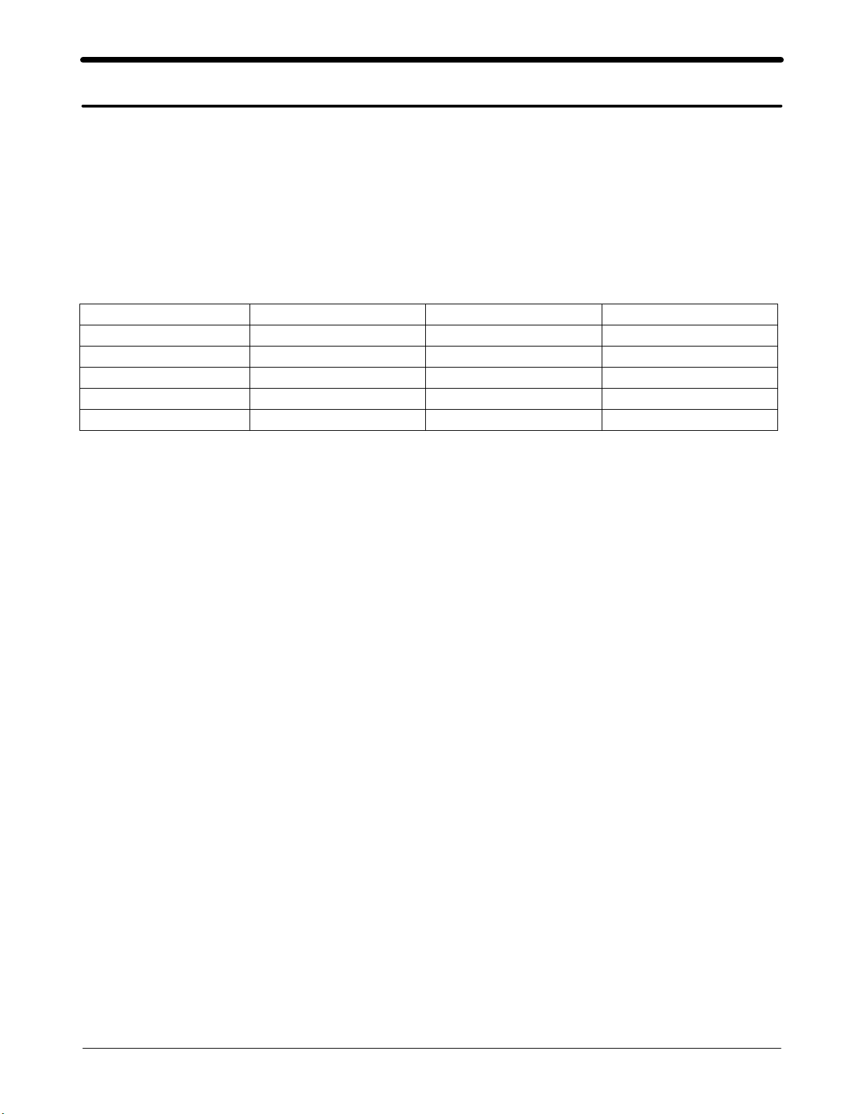
- ANTENNA SWITCH Control Losic (F101)→Truth Table
VC1 VC2 VC3
Tx Mode (GSM900) H L L
Tx Mode (DCS1800/1900) L H L(H)
Rx Mode (GSM900) L L L
Rx Mode (DCS1800) L L L
Rx Mode (PCS1900) L L H
- TRANSCEIVER (U102)
This chip is fully integrated GSM GPRS tri-band transceiver with transmit baluns(balanced-unbalanced matching devices) ,
loop filters and most of the passive component in it.
And also fully integrated fractional N RF synthesizer with AFC control possibility, RF VCO with integrated supply
regulator. Semi integrated reference oscillator with integrated supply regulator.
RF Receiver front-end amplifies the E-GSM900, DCS1800 and PCS1900 aerial signal, convert the chosen channel
down to a low IF of 100kHz.
In IF section, further amplifies the wanted channel output level to the desired value and rejects DC.
-PAM(PAM101)
The module consists of two separated line-ups, one for low band(LB 850/900) and one for high band(HB,1800/1900) with
input and output matching and internal power detection function and power control loop in GSM mode.
in GSM mode, the internal power control circuit ensures a stable power output, set by the level of V
compensate variations of supply voltage, input power and temperature, with a control range fully compaliant with ETSI
tome mask and power spectrum requirements
in EDGE mode the output power is controlled by the input power. The V
controlling the quiescent current of the final RF-statges of both line-ups.
signal is used to control the efficiency by
REF
stabilsed to
DAC
2-1-2. TX PART
The transmitter is fully differential using a direct up conversion architecture. It consists of a signal side band
power up mixer. Gain is controlled by 6 dB via 3-wire serial bus programing. The fully integrated VCO and power
mixer achieve LO suppression, quadrature phase error, quadrature amplitude balance and low noise floor specification.
Output matching/balun components drive a standard 50 ohms single ended load.
2-1
SAMSUNG Proprietary-Contents may change without notice
This Document can not be used without Samsung's authorization
Page 2

Circuit Description
2-2. Baseband Circuit description of SGH-X670
2-2-1. PCF50603 (U400)
- Power Management
Eight low-dropout regulators designed specifically for GSM applications power the terminal and help ensure optimal
system performance and long battery life. A programmable boost converter provides support for 1.8V, 3.0V SIMs,
while a self-resetting, electronically fused switch supplies power to external accessories. Ancillary support functions,
such as RTC module and High Voltage Charge pump, Clock generator, aid in reducing both board area and system
complexity.
I2C BUS serial interface provides access to control and configuration registers. This interface gives a microprocessor
full control of the PCF50603 and enables system designers to maximize both standby and talk times.
Supervisory functions. including a reset generator, an input voltage monitor, and a temperature sensor, support reliable
system design. These functions work together to ensure proper system behavior during start-up or i n the event of a
fault condition(low microprocessor voltage, insufficient battery energy, or excessive die temperature).
- Backlight Brightness Modulator
The Backlight Brightness Modulator (BBM) contains a programmable Pulse-width modulator (PWM) and FET to
modulate the intensity of a series of LEDs or to control a DC/DC converter that drives LCD backlight.
This phone (SGH-X670) use PWM control to contrast the backlight brightness.
- Clock Generator
The Clock Generator (CG) generates all clocks for internal and external usage. The 32.768 kHz crystal oscillator
provides an accurate low clock frequency for the PCF50603 and other circuitry.
2-2-2. LCD Connector
LCD is consisted of main LCD(color 65K UFB LCD) and sub LCD(color 65K UFB LCD)
Chip select signals in the U305, LCD_MAIN_CS, LCD_SUB_CS can enable LCD. DIM-EN signal enables white LED of
main LCD. These signal is from U200.
16-bit data lines(LD(0)~LD(15)) transfers data and commands to LCD. Data and commands use "RS" signal. If this signal
is high, Inputs to LCD are commands. If it is low, Inputs to LCD are data. The signal which informs the input or output
state to LCD, is required. But this system is not necessary this signal. So "L_WR" signal is used to write data or
commands to LCD. Power signals for LCD are "VDD_IO_HIGH".
2-2-3. BLUE TOOTH
This system uses Blue Tooth module, UGNZ6XG23A, ALPS. This has signals, "BT_INT"(Interrupt signal), "RXD2"(input
data) and "TXD2"(output data), PCM control signal(DCL[PCMCLK], DO[PCM_IN], DU[PCM_OUT], FSC[PCM_SYNC])
These signals are connected to PCF5213EL1EL1.
2-2
SAMSUNG Proprietary-Contents may change without notice
This Document can not be used without Samsung's authorization
Page 3

Circuit Description
2-2-4. Key
This is consisted of key interface pins KEY_ROW(0:4) and KEY_COL(0:4) in PCF5213EL1. These signals compose the
matrix. Result of matrix informs the key status to key interface in the PCF5213EL1. Power on/off key is seperated from
the matrix. So power on/off signal is connected with PCF50603 to enable PCF50603. Key LED is consisted of 12 LEDs.
key LED use the 3.3V LDO(U700) for a supply voltage. KEY_LED_ON signal enables eight white LED.
"FLIP" informs the status of slide (up or down) to the PCF5213EL1. This uses the hall effect IC, EM-1681-FT(U503).
A magnet under LCD enables EM-1681-FT.
2-2-5. EMI ESD Filter
This system uses the EMI ESD filter, U500 to protect noise from IF CONNECTOR part.
2-2-6. IF connetor(IFC500)
It is 18-pin connector. They a re designed to use VBAT, V_EXT_CHARGE, USB_D+, +VBUS, USB_D-, TXD1, RXD1,
AUX_ON, EXT1, EXT2 and GND. They connected to power supply IC, microprocessor and signal processor IC.
2-2-7. Battery Charge Management
A complete constant-current/constant-voltage linear charger for single cell lithium-ion batteries.
If TA connected to phone, "V_EXT_CHARGE" enable charger IC and supply current to battery.
When fault condition caused, "CHG_ON" signal level change low to high and charger IC stop charging process.
2-2-8. Audio
HFR_P and HFR_N from PCF5213EL1 are connected to the main speaker via analog switches. MIC_P and MIC_N
are connected to the main MIC as well. EAR1 is the source of External Speaker. YMU762 is a s ynthesizer LSI for
mobile phones. This LSI has a built-in speaker amplifier for outputting sounds that are used by mobile phones in addition
to game sounds and ringing melodies that are replayed by a synthesizer.
The synthesizer section adopts“stereophonic hybrid synthesizer system”that are given advantages of both FM
synthesizers and Wave Table synthesizers to allow simultaneous generation of up to 32 FM voices and 32 Wave
Table voices. It provides simultaneous generation of up to 40 tones by stereophonic hybrid synthesizer.
YMU762 has built a speaker amplifier of which maximum out is 580 mW at SPVDD=3.6V in this device.
There is Stereophonic analog output for Headphone.
2-2-9. Memory(UME303)
This system uses Samsung's memory, KAP17VG00M. The KAP17VG00M is a Multi Chip Package Memory which
combines 256Mbit Synchronous Burst Multi Bank NOR Flash Memory and 256Mbit NAND Flash and
128Mbit Synchronous Burst UtRAM.
It has 16 bit data line, HD[1~16] which is connected to PCF5213EL1 and MV3017SAQ, also has 24 bit address lines,
HA[1~24]. There are 3 chip select signals, CS0n_FLASH, CS4n_NAND, and CS1n_RAM.
In the Writing process, WEn is fallen to low and it enables writing process to operate. During reading process,
OEn is fallen to low and it enables reading process to operate. Each chip select signals in the PCF5213EL1 choose
different memories.
2-3
SAMSUNG Proprietary-Contents may change without notice
This Document can not be used without Samsung's authorization
Page 4

Circuit Description
2-2-10. PCF5213EL1(UCP200)
The PCF5213EL1 is mainly composed of embeded DSP and ARM core. The DSP subsystem includes the Saturn
DSP core with embedded RAM and ROM, and a set of peripherals. It has 24kx16 bits PRAM, 104k*16 bits,
32k*16 XYRAM and 63k*16 XYROM in the DSP.
The ARM946E-S consists of an ARM9E-S processor core, 8 kbyte instruction cache and 8 kbyte data cache,
tghtly-coupled ITCM(Instruction Tightly Coupled Memory) and DTCM(Data Tightly Coupled Memory) memories, a
memory protection unit, and an AMBA(Advanced Microcontroller Bus Architecture) AHB(Advanced
High-performance Bus) bus interface with a write buffer.
HD(0:15), data lines and HA(0:23), address lines are connected to KAP17SG00A (memory), MV3018B (image dsp)
and YMU762 (melody IC). It has 64 kbyte SC RAM (0.5 Mbit) and 32 kbyte SC program ROM for bootstrap
loader in the ARM core.
HD(0:15), data lines and HA(0:23), address lines are connected to memory and YMU762 to communicate.
MV3018B(Camera DSP Chip) controls the communication between ARM core and DSP core.
OEn, WEn control the access of memory. KROW, and KCOL recognize the key string input status.
It has J-TAG control pins (TDI/TDO/TCK) for ARM and DSP core. J-SEL signal controls different access to ARM
and DSP core.
ADC(Analog to Digital Convertor) receives the condition of temperature, battery type and battery voltage.
2-2-11. TOH2600DGI4KRA (26MHz)(TCX101)
This system uses the 26MHz VCTCXO; TOH2600DGI4KRA. AFC control signal form PCF5213EL1 controls
frequency from 26MHz x-tal. It generates the clock frequency. This clock is connected to PCF5213EL1, YMU762 and
UAA3587C2.
2-2-12. Camera DSP(MV3017SAQ)(U305)
MV3018SAQ provides rich video functions up to 30-frame display with minimized tasks in the handset main processor
as well as hardware based real-time JPEG compression and decompression. MV3018SAQ directly transmits and
previews the RGB data to the LCD graphic memory by processing the sensor output data according to the
handset's command. It can save the raw RGB data up to VGA resoultion into its image buffer and allows the
host processor to download with scalable sized compressed data.
It utilizes 16 bit data bus for communication with the main processor, including bus interface types.
2-2-13. FM Radio (TEA5761UK)(U603)
The TEA5761 is a single chip electronically tuned FM stereo radio for low voltage application with fully integrated IF
selectivity and demodulation.
TEA5761UK provide FM mixer for conversion of the US/Europe (87.5 MHz to 108 MHz) and Japanese FM band (76
MHz to 90 MHz) to IF.Preset tuning to receive Japanese TV audio up to 108 MHz, raster 100 kHz. and is connected to
PCF5213EL1 of I2C.
2-4
SAMSUNG Proprietary-Contents may change without notice
This Document can not be used without Samsung's authorization
 Loading...