

Page 1

8mm CAMCORDER
VP-A12/VP-A15
VP-A17/VP-A18
SERVICE
1. Precautions
2. Reference Information
3. Product Specifications and
Comparison Chart
4. Disassembly and Reassembly
5. Alignment and Adjustment
6. Exploded View and Parts List
7. Electrical Parts List
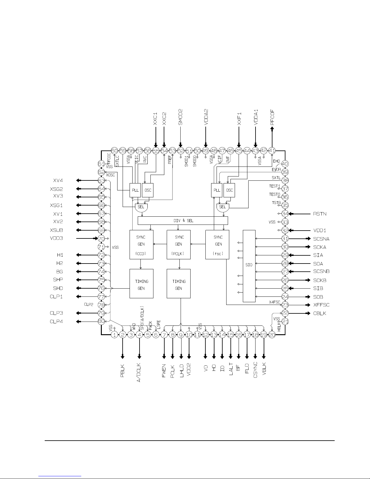
8. Block Diagrams
9. PCB Diagrams
10. Wiring Diagram
11. Schematic Diagrams
Manual
8mm CAMCORDER
CONTENTS
For mechanical disassembly and adjustment, refer to the “Mechanical Manual”
(DE-6 AD68-30200A).
PUSH
© Samsung Electronics Co., Ltd. APR. 1997 AD68-20274A
Page 2

Samsung Electronics 1-1
1. Precautions
1. Be sure that all of the built-in protective devices are
replaced. Restore any missing protective shields.
2. When reinstalling the chassis and its assemblies, be
sure to restore all protective devices, including :
control knobs and compartment covers.
3. Make sure that there are no cabinet openings
through which people--particularly children
--might insert fingers and contact dangerous
voltages. Such openings include the spacing
between the picture tube and the cabinet mask,
excessively wide cabinet ventilation slots, and
improperly fitted back covers.
If the measured resistance is less than 1.0 megohm
or greater than 5.2 megohms, an abnormality exists
that must be corrected before the unit is returned
to the customer.
4. Leakage Current Hot Check (See Fig. 1) :
Warning : Do not use an isolation transformer
during this test. Use a leakage current tester or a
metering system that complies with American
National Standards Institute (ANSI C101.1,
Leakage Current for Appliances), and Underwriters
Laboratories (UL Publication UL1410, 59.7).
5. With the unit completely reassembled, plug the AC
line cord directly the power outlet. With the unitÕs
AC switch first in the ON position and then OFF,
measure the current between a known earth
ground (metal water pipe, conduit, etc.) and all
exposed metal parts, including : antennas, handle
brackets, metal cabinets, screwheads and control
shafts. The current measured should not exceed
0.5 milliamp. Reverse the power-plug prongs in the
AC outlet and repeat the test.
6. X-ray Limits :
The picture tube is designed to prohibit X-ray
emissions. To ensure continued X-ray protection,
replace the picture tube only with one that is the
same type as the original.
Fig. 1 AC Leakage Test
7. Antenna Cold Check :
With the unitÕs AC plug disconnected from the
AC source, connect an electrical jumper across the
two AC prongs. Connect one lead of the ohmmeter
to an AC prong.
Connect the other lead to the coaxial connector.
8. High Voltage Limit :
High voltage must be measured each time
servicing is done on the B+, horizontal deflection
or high voltage circuits.
Heed the high voltage limits. These include the
X-ray protection Specifications Label, and the
Product Safety and X-ray Warning Note on the
service data schematic.
9. Some semiconductor (Òsolid stateÓ) devices are
easily damaged by static electricity.
Such components are called Electrostatically
Sensitive Devices (ESDs); examples include
integrated circuits and some field-effect transistors.
The following techniques will reduce the
occurrence of component damage caused by static
electricity.
10. Immediately before handling any semiconductor
components or assemblies, drain the electrostatic
charge from your body by touching a known
earth ground. Alternatively, wear a discharging
Wrist-strap device. (Be sure to remove it prior to
applying power--this is an electric shock
precaution.)
Device
Under
Test
(Reading should
not be above
0.5mA)
Leakage
Currant
Tester
Earth
Ground
Test all
exposed metal
surfaces
Also test with
plug reversed
(using AC adapter
plug as required)
2-Wire Cord
Page 3

Precautions
1-2 Samsung Electronics
11. High voltage is maintained within specified limits
by close-tolerance, safety-related components and
adjustments. If the high voltage exceeds the
specified limits, check each of the special
components.
12. Design Alteration Warning :
Never alter or add to the mechanical or electrical
design of this unit. Example : Do not add
auxiliary audio or video connectors. Such
alterations might create a safety hazard. Also, any
design changes or additions will void the
manufacturerÕs warranty.
13. Hot Chassis Warning :
Some TV receiver chassis are electrically
connected directly to one conductor of the AC
power cord. If an isolation transformer is not
used, these units may be safely serviced only if
the AC power plug is inserted so that the chassis
is connected to the ground side of the AC source.
To confirm that the AC power plug is inserted
correctly, do the following : Using an AC
voltmeter, measure the voltage between the
chassis and a known earth ground. If the reading
is greater than 1.0V, remove the AC power plug,
reverse its polarity and reinsert. Re-measure the
voltage between the chassis and ground.
14. Some TV chassis are designed to operate with 85
volts AC between chassis and ground, regardless
of the AC plug polarity. These units can be safely
serviced only if an isolation transformer inserted
between the receiver and the power source.
15. Never defeat any of the B+ voltage interlocks.
Do not apply AC power to the unit (or any of its
assemblies) unless all solid-state heat sinks are
correctly installed.
16. Always connect a test instrumentÕs ground lead to
the instrument chassis ground before connecting
the positive lead; always remove the instrumentÕs
ground lead last.
17. Observe the original lead dress, especially near
the following areas : Antenna wiring, sharp
edges, and especially the AC and high voltage
power supplies. Always inspect for pinched, outof-place, or frayed wiring. Do not change the
spacing between components and the printed
circuit board. Check the AC power cord for
damage. Make sure that leads and components
do not touch thermally hot parts.
18. Picture Tube Implosion Warning :
The picture tube in this receiver employs
Òintegral implosionÓ protection. To ensure
continued implosion protection, make sure that
the replacement picture tube is the same as the
original.
19. Do not remove, install or handle the picture tube
without first putting on shatterproof goggles
equipped with side shields. Never handle the
picture tube by its neck. Some Òin-lineÓ picture
tubes are equipped with a permanently attached
deflection yoke; do not try to remove such
Òpermanently attachedÓ yokes from the picture
tube.
20. Product Safety Notice :
Some electrical and mechanical parts have special
safety-related characteristics which might not be
obvious from visual inspection. These safety
features and the protection they give might be
lost if the replacement component differs from the
original--even if the replacement is rated for
higher voltage, wattage, etc.
Components that are critical for safety are
indicated in the circuit diagram by shading,
( or ).
Use replacement components that have the same
ratings, especially for flame resistance and
dielectric strength specifications. A replacement
part that does not have the same safety
characteristics as the original might create shock,
fire or other hazards.
Page 4

Samsung Electronics 2-1
2. Reference Information
2-1 Servicing Jigs and Special Tools
2-1-1 Servicing Jigs
Part No.
68140-500-037
Jig Item
Extension
Cable 1
Specification
Pin 36
Main board CCD board
DC/DC Converter board
Remarks
Troubleshooting
Description
CN501 CN901
68140-500-033 68140-500-035 68140-500-038
Extension Cable 1
Extension Cable 2
Extension Cable 3
68140-500-035
Extension
Cable 2
Pin 40
Troubleshooting
CN203
68140-500-038
Extension
Cable 3
Pin 40
Troubleshooting
CNP01 CND02
Audio board
CN701
Page 5

Reference Information
2-2 Samsung Electronics
2-4-2 Extension Cable Connections
ASS'Y DC/DC
CONVERTER
EXTENSION CABLE 1
ASS'Y LENS ZOOM
ASS'Y AUDIO BOARD
ASS'Y MAIN BOARD
EXTENSION CABLE 3
EXTENSION CABLE 2
CN501
CN901
ASS'Y CCD BOARD
CND02
CNP01
CN701
CN203
Page 6

Reference Information
Samsung Electronics 2-3
2-2 IC Blocks
2-2-1 IC101(M52369FP)
Page 7

Reference Information
2-4 Samsung Electronics
2-2-2 IC601(CXP87240A)
Page 8

Reference Information
Samsung Electronics 2-5
2-2-3 IC701(AN3996NFHP-Mono)
Page 9

Reference Information
2-6 Samsung Electronics
2-2-4 IC701(AN2980A-Stereo)
Page 10

Reference Information
Samsung Electronics 2-7
2-2-5 IC201(CXA1700R)
Page 11

Reference Information
2-8 Samsung Electronics
2-2-6 IC501(KA8322)
Page 12

Reference Information
Samsung Electronics 2-9
2-2-7 ICS15(CXP811P24R)
Page 13
Reference Information
2-10 Samsung Electronics
2-2-8 ICP01(KS7213)
Page 14

Reference Information
Samsung Electronics 2-11
2-2-9 ICP02(KA7307)
Page 15

Reference Information
2-12 Samsung Electronics
2-2-10 ICP08(KS7306)
Page 16

Reference Information
Samsung Electronics 2-13
2-2-11 ICP06(AD876)
Page 17

Reference Information
2-14 Samsung Electronics
2-2-12 ICP09(UPD78018)
Page 18

Reference Information
Samsung Electronics 2-15
2-2-13 ICZ07(KS7314)
Page 19

Reference Information
2-16 Samsung Electronics
2-2-14 ICE01(KA7007)
Page 20

Reference Information
Samsung Electronics 2-17
2-2-15 ICE01(CXA1854AR)-CVF
Page 21

Reference Information
2-18 Samsung Electronics
MEMO
Page 22

Samsung Electronics 3-1
3. Product Specifications and Comparison Chart
3-1 Product Specifications
Design and specifications are subject to change without notice.
Operation
Description
SYSTEM
Recording systems Video : 2 rotary heads, helical FM scanning; Audio : FM system
Video signal PAL colour, CCIR standard
Cassette format 8 mm
Tape speed SP mode (Standard Play) : approx. 20.051 mm/sec
Recording/playback time SP mode (Standard Play) : 1 hour 30 minutes (P5-90)
Fast-forward/rewind time Approx. 4 min. (P5-60)
Image device CCD (Charge Coupled Device)
Viewfinder VP-A12/VP-A17 : Black and White electronic viewfinder
VP-A15/VP-A18 : Colour electronic viewfinder
Lens VP-A12/VP-A15 : Combined 16X power zoom and 32X digital zoom
VP-A17/VP-A18 : Combined 16X power zoom and 32X digital zoom
f=3.9~62.4mm, F1.4 auto wide macro; filter diameter 46 mm.
Automatic focus system Inner
Colour temperature Auto
Lighting > 300 lux (28 footcandles)
Aperture correction Automatic with back light adjustment
INPUT/OUTPUT CONNECTORS
Video output Phono jack, 1Vp-p, 75 ohms, unbalanced, SYNC negative
Audio output Phono jack, 7.5dBs for an output impedance of less than 2.2 Kohms
RFU DC OUT Special mini-jack, 5V DC
Earphone output Minijack, 8 ohms
Ext Mic. Minijack, ø3.5 mm
GENERAL
Power requirement AC power adaptor (6.0V) ; battery pack (6.0V)
Power consumption VP-A12/VP-A15 : 5.0W, VP-A17/VP-A18 : 5.7W (in camera mode)
Tripod attachment thread Attachment screw less than 9mm long
Microphone VP-A12 : Electric condensor microphone, omni-directional, manual type
VP-A15/A17/A18 : Electric condensor microphone, omni-directional, stereo type
Temperature range Operation : 0°C to 40°C (32°F to 104°F); storage : -20°C to 60°C (-4°F to 140°F)
Dimensions/weight Appros. 110 X 114 X 224 mm (4.3 X 4.5 X 8.8 inches) ; approx. 760 g (1.65 lbs)
including lens cap, excluding battery pack and cassette
Page 23

Product Specifications
3-2 Samsung Electronics
3-2 Comparison Chart
MICROPHONE MONO STEREO STEREO STEREO
VIEWFINDER EVF CVF EVF CVF
D.ZOOM X24 D.ZOOM X24 D.ZOOM X64 D.ZOOM X64 D.ZOOM
EIS X X O O
WIDE X X O O
MODEL
FUNCTION
VP-A12 VP-A15 VP-A17 VP-A18 REMARK
Page 24

Samsung Electronics 4-1
4. Disassembly and Reassembly
4-1 Cabinet Disassembly
1 APPLY POWER AND OPEN
THE HOUSING ASS'Y.
2 REMOVE 2 SCREWS.
( BH ; M 1.7 X 5 )
3
REMOVE THE ASS'Y COVER HOUSING
IN THE DIRECTION OF ARROW.
4-1-1 Ass’y Cover Housing Removal
Fig. 4-1 Ass’y Cover Housing Removal
Page 25

Disassembly and Reassembly
4-2 Samsung Electronics
1 REMOVE ASS'Y CASE TOP BY GENTLELY RELEASING
2 LOCKING TABS WITH A SMALL SCREW DRIVER.
(SEE DETAIL "A")
2 LOCKING TABS
PRECISION
SCREW DRIVER
DETAIL "A"
DETAIL "B"
REASSEMBLY : PUT THE 7 TABS INTO THE SLOT, WHILE SLIDING
IT AS SHOWN IN DETAIL "B".
4-1-2 Ass’y Case Top Removal
Fig. 4-2 Ass’y Case Top Removal
Page 26

Disassembly and Reassembly
Samsung Electronics 4-3
1 REMOVE 3 SCREWS.
( BH ; M2 X 5 )
3 REMOVE THE ASS'Y FRONT
IN THE DIRECTION
OF ARROW .
2 OPEN THE COVER JACK IN
THE DIRECTION OF ARROW .
4 DISCONNECT THE FPC FROM
THE CN702 OF ASS'Y AUDIO BOARD.
1
1
LEVER - BUILT
NOTE : WHEN REASSEMBLING, PUSH THE LEVER - BUILT
TOWARD ARROW AND THEN REINSTALL IT.
C
C
B
A
A
B
4-1-3 Ass’y Front Removal (1)
Fig. 4-3 Ass’y Front Removal (1)
Page 27

Disassembly and Reassembly
4-4 Samsung Electronics
1 REMOVE 2 SCREWS.
( TAP ; 2X4 )
5 REMOVE 2 SCREWS.
( TAP ; 2X4 )
REMOVE THE HOLDER LENS COVER.
7
4
11
2 DISCONNECT THE ASS'Y FPC MIC
FROM THE CN761 OF ASS'Y MIC BOARD.
DISCONNECT THE CONNECTOR
FROM THE CN763 OF
ASS'Y MIC BOARD.
ASS'Y MIC
BOARD
COVER ROTATE
COVER
LENS A
COVER LENS B
HOLDER
LENS COVER
ASSEMBLING
POINT
A
C
B
D
E
14
REMOVE THE ASS'Y MIC
IN THE DIRECTION OF
ARROW .
E
8
SPRING COVER (2)
3 REMOVE THE FPC ASS'Y MIC
IN THE DIRECTION OF
ARROW .
A
REMOVE THE ASS'Y MIC BOARD
IN THE DIRECTION OF ARROW .
6
B
10
REMOVE 3 SCREWS.
( TAP ; 2X4 )
9
10
13
REMOVE 2 SCREWS.
( TAP TITE ; BH)
10
11
a
b
7 REMOVE THE SPRING COVER (2) FROM THE COVER ROTATE OF HOOK AND HOLDER LENS COVER OF HOOK .
a
b
c
8 REMOVE THE COVER ROTATE IN THE DIRECTION OF ARROW AFTER PUSHING THE 3 TABS .
C
c
SPRING COVER
e
d
f
REMOVE THE SPRING COVER FROM THE HOLDER LENS COVER HOOK , AND HOLDER LENS A HOOK .
9
e
d
f
g
REMOVE THE COVER LENS B AND COVER LENS A FROM
THE BOSS IN THE DIRECTION OF ARROW .
12
D
g
4-1-4 Ass’y Front Removal (2)
Fig. 4-4 Ass’y Front Removal (2)
Page 28

Disassembly and Reassembly
Samsung Electronics 4-5
1
1 REMOVE 4 SCREWS.
( BH ; M2 X 5 )
2 REMOVE THE UNIT CASE RIGHT IN THE DIRECTION OF ARROW .
3 DISCONNECT THE FPC FROM
THE CN201 OF ASS'Y MAIN BOARD.
1
1
A
A
4-1-5 Unit Case Right Removal
Fig. 4-5 Unit Case Right Removal
Page 29

Disassembly and Reassembly
4-6 Samsung Electronics
1 REMOVE 3 SCREWS.
( BH ; M2 X 5 )
COVER LI BATTERY
KNOB - EJECT
2 REMOVE 1 SCREW.
( SPACER ; TAP 2 X 8.2 )
3 REMOVE 1 SCREW.
( TAP ; 2 X 4 )
1
A
< DITAIL "A" >
< DITAIL "B" >
1
4 REMOVE THE CASE LEFT
ASSEMBLY IN THE DIRECTION
OF ARROW .
5 DISCONNECT THE FPC FROM THE
CN502 OF ASS'Y MAIN BOARD.
ASSEMBLING
POINT
A
B
A
CN502
A
NOTE 1 : WHEN DISASSEMBLING, TAKE CARE NOT TO DAMAGE
OR LOSS THE . (SEE DETAIL "B")
NOTE 2 : WHEN REASSEMBLING,
1) OPEN THE COVER LI BATTERY.
2) PUSH THE KNOB - EJECT IN THE DIRECTION OF
ARROW .
3) INSTALL IT AS SHOWN IN DETAIL "A".
B
4-1-6 Ass’y Case Left Removal (1)
Fig. 4-6 Ass’y Case Left Removal (1)
Page 30

Disassembly and Reassembly
Samsung Electronics 4-7
2
REMOVE 2 SCREWS.
( TAP ; 2 X 6 )
3
REMOVE THE EVF/CVF ASS'Y IN THE
DIRECTION OF ARROW .
1
ASS'Y EVF/CVF
A
A
1 CVF : DISCONNECT THE FPC FROM THE CN807 OF UNIT FUNCTION DSE BOARD.
EVF : DISCONNECT THE LEAD CONNECTOR ASS'Y FROM THE CN804 OF UNIT FUNCTION DSE BOARD.
CN804
CN807
4-1-7 Ass’y EVF/CVF Removal
Fig. 4-7 Ass’y EVF/CVF Removal
Page 31

Disassembly and Reassembly
4-8 Samsung Electronics
4 REMOVE 2 SCREWS.
( TAP ; 2X4 )
2
REMOVE 2 SCREWS.
( TAP ; 2X4 )
2 REMOVE THE UNIT FUNCTION EAP BOARD
IN THE DIRECTION OF ARROW .
11
REMOVE 4 SCREWS.
( TAP ; 2X4 )
12
REMOVE THE UNIT FUNCTION DSE BOARD
IN THE DIRECTION OF ARROW .
8
DISCONNECT THE CONNECTOR
FROM CN802 OF UNIT
FUNCTION BLC BOARD.
1
DISCONNECT THE CONNECTOR
FROM CN808 OF UNIT
FUNCTION EAP BOARD.
10
REMOVE 2 SCREWS.
( TAP ; 2X4 )
REMOVE THE UNIT FUNCTION BLC BOARD
IN THE DIRECTION OF ARROW .
5
DISCONNECT THE CONNECTOR
FROM CN801 OF UNIT
FUNCTION VCR BOARD.
6
REMOVE 2 SCREWS.
( TAP ; 2X4 )
7
REMOVE THE UNIT FUNCTION VCR BOARD
IN THE DIRECTION OF ARROW .
3
A
C
D
B
UNIT FUNCTION BLC
BOARD
UNIT FUNCTION VCR
BOARD
UNIT FUNCTION
EAP BOARD
UNIT FUNCTION
DSE BOARD
A
B
C
D
9
4-1-8 Ass’y Case Left Removal (2)
Fig. 4-8 Ass’y Case Left Removal (2)
Page 32

Disassembly and Reassembly
Samsung Electronics 4-9
5 DISCONNECT THE 2 FPC FROM
THE CN501, CN101 OF ASS'Y MAIN BOARD.
6 DISCONNECT
8 CONNECTORS
1 REMOVE 1 SCREW.
( BH ; M 2 X 3 )
3 REMOVE 2 SCREWS.
( BH ; M 2 X 3 )
7 REMOVE THE ASS'Y MAIN BOARD AND
ASS'Y CAMERA IN THE DIRECTION OF
ARROW .
4 REMOVE 1 SCREW.
( SPACER ; M 2 X 8.2 )
2 REMOVE THE ASS'Y DC/DC CONVERTER
IN THE DIRECTION OF ARROW .
A
B
B
A
W501
W502
W501
W502
ASS'Y 8MM DECK
4-1-9 Ass’y 8mm Deck, Ass’y Main Board and DC/DC Converter Removal
Fig. 4-9 Ass’y 8mm Deck, Ass’y Main Board and DC/DC Converter Removal
Page 33

Disassembly and Reassembly
4-10 Samsung Electronics
3 REMOVE 2 SCREWS.
( SPACER ; M2 X 8.2 )
1 REMOVE 1 SCREW.
( SPACER ; M2 X 8.2 )
6 REMOVE 3 SCREWS.
( TAP ; 2 X 4 )
9 PULL THE ASS'Y CCD BOARD IN THE DIRECTION OF
ARROW .
10 DESOLDER
DESOLDER
11 REMOVE 2 SCREWS.
( BH ; M2 X 3 )
8 REMOVE 2 SCREWS.
( TAP ; 2 X 6 )
7 REMOVE THE BRACKET LENS
IN THE DIRECTION OF ARROW .
5 REMOVE THE ASS'Y MAIN BOARD
IN THE DIRECTION OF ARROW .
6
2
CN701
REMOVE THE ASS'Y AUDIO BOARD
IN THE DIRECTION OF ARROW .
CCD
ASS'Y CCD
BOARD
6
CN703
D
D
C
B
A
A
B
C
CN702
(HI-BAND MODEL ONLY)
4
4-1-10 Ass’y Main Board and Ass’y Camera Removal
Fig. 4-10 Ass’y Main Board and Ass’y Camera Removal
Page 34

Disassembly and Reassembly
Samsung Electronics 4-11
1 REMOVE THE BODY LENS IN THE
DIRECTION OF ARROW .
7 REMOVE THE ASS'Y EVF BOARD
IN THE DIRECTION OF ARROW .
3 REMOVE THE COVER - CASE EVF
IN THE DIRECTION OF ARROW .
4 REMOVE 1 SCREW.
( BH ; M2X4 )
5 REMOVE 1 SCREW.
( TAP ; M2X4 )
2 REMOVE 2 SCREWS.
( TAP ; 2X4 )
6 REMOVE THE CASE - LEFT
EVF IN THE DIRECTION OF
ARROW .
A
D
B
C
B
A
D
C
4-1-11 Ass’y EVF Removal
Fig. 4-11 Ass’y EVF Removal
Page 35

Disassembly and Reassembly
4-12 Samsung Electronics
1 REMOVE THE BODY LENS IN THE
DIRECTION OF ARROW .
7 REMOVE THE ASS'Y CVF BOARD AND ASS'Y B/L
BOARD IN THE DIRECTION OF ARROW .
3 REMOVE THE COVER - CASE EVF
IN THE DIRECTION OF ARROW .
4 REMOVE 1 SCREW.
( BH ; M2X4 )
5 REMOVE 1 SCREW.
( TAP ; M2X4 )
2 REMOVE 2 SCREWS.
( TAP ; 2X4 )
6 REMOVE THE CASE - LEFT
EVF IN THE DIRECTION OF
ARROW .
B
A
B
D
C
C
D
ASS'Y CCD
BOARD
LCD DISPLAY
ASS'Y B/L BOARD
A
4-1-12 Ass’y CVF Removal
Fig. 4-12 Ass’y CVF Removal
Page 36

Disassembly and Reassembly
Samsung Electronics 4-13
4-2 Circuit Boards Location
UNIT FUNCTION VCR
UNIT FUNCTION BLC
ASS'Y FPC MIC
ASS'Y EVF/CVF BOARD
ASS'Y CCD BOARD
ASS'Y AUDIO
BOARD
ASS'Y A/V JACK
ASS'Y MIC
BOARD
UNIT FUNCTION DSE
UNIT FUNCTION EAP
ASS'Y DC/DC
CONVERTER
ASS'Y MAIN BOARD
Fig. 4-13 Circuit Boards Location
Page 37

Fig. 4-14 Circuit Boards Location
Disassembly and Reassembly
4-14 Samsung Electronics
4-3 Connector Diagrams
4-3-1 Diagram(1)
FROM/TO UNIT
FUNCTION DSE
ASS'Y FPC MIC
ASS'Y MIC BOARD
2
12
1
4
3
7
5
6
8
9
10
11
13
14
15
16
17
18
19
ASS'Y DC/DC
CONVERTER
ASS'Y MAIN
BOARD
ASS'Y AUDIO BOARD
ASS'Y 8MM DECK
ASS'Y A/V JACK
7
9
, : Hi-BAND MODEL ONLY
NO
CONN.WAFER
DIRECTION
CONN.WAFERNOCONN.WAFER
DIRECTION
CONN.WAFER
LOCA-NO LOCA-NO LOCA-NO LOCA-NO
1 W502 FROM/TO ASS’Y MAIN BOARD CN101 2 W501 FROM/TO ASS’Y MAIN BOARD CN501
3 CN501 FROM/TO ASS’Y 8MM DECK W501 4 CN101 FROM/TO ASS’Y 8MM DECK W502
5 CN203
A
SS’Y MAIN BOARD ASS’Y AUDIO BOARD
CN701 6 CNP01
ASS’Y MAIN BOARD ASS’Y CCD BOARD
CND02
7 CN202
A
SS’Y MAIN BOARD ASS’Y AUDIO BOARD
CN703 8 CN701
ASS’Y AUDIO BOARD ASS’Y MAIN BOARD
CN203
9 CN703
A
SS’Y AUDIO BOARD ASS’Y MAIN BOARD
CN202 10 CN702
ASS’Y AUDIO BOARD ASS’Y FPC MIC
-
11 CN201
ASS’Y MAIN BOARD ASS’Y AV JACK
- 12 CN901
ASS’Y DC/DC CONVERTER ASS’Y MAIN BOARDCN503
13 CN503
ASS’Y MAIN BOARD ASS’Y DC/DC CONVERTER
CN901 14 CN502
ASS’Y MAIN BOARD UNIT FUNCTION DSE
CN805
15 - ASS’Y AV JACK ASS’Y MAIN BOARD CN201 16 CN761 FROM/TO ASS’Y FPC MIC 17 - FROM/TO ASS’Y MIC BOARD CN761 18 -
ASS’Y FPC MIC ASS’Y AUDIO BOARD
CN702
19 CND01
ASS’Y CCD BOARD ASS’Y MAIN BOARD
CNP01
Page 38

Disassembly and Reassembly
Samsung Electronics 4-15
4-3-2 Diagram(2)
NO
CONN.WAFER
DIRECTION
CONN.WAFER
LOCA-NO LOCA-NO
1 CN805 UNIT FUNCTION DSE ASS’Y MAIN BOARD CN502
2 CN804 UNIT FUNCTION DSE ASS’Y EVF 3 CN807 UNIT FUNCTION DSE ASS’Y CVF 4 CN806 UNIT FUNCTION DSE UNIT FUNCTION VCR CN801
5 CN808 UNIT FUNCTION EAP UNIT FUNCTION DSE CN806
6 CN802 UNIT FUNCTION BLC UNIT FUNCTION DSE CN806
7 CN801 UNIT FUNCTION VCR UNIT FUNCTION DSE CN806
8 CN806 UNIT FUNCTION DSE UNIT FUNCTION EAP CN808
9 CN806 UNIT FUNCTION DSE UNIT FUNCTION BLC CN802
ASS'Y EVF ONLY
ASS'Y CVF ONLY
ASS'Y EVF/CVF
1
3
2
4
5
7
6
UNIT FUNCTION
EAP
UNIT FUNCTION BLC
UNIT FUNCTION
DSE
UNIT FUNCTION
VCR
9
8
Page 39

Disassembly and Reassembly
4-16 Samsung Electronics
MEMO
Page 40

Samsung Electronics 5-1
5. Alignment and Adjustment
5-1 Mechanical Adjustment
1. Refer to mechanical manual ÒDE-6 (AD68-30200A)Ó for the adjustment and checks of mechanism section.
2. Short between pin 12 of IC601 and GND in order to set the TEST mode (Track Shift Mode).
3. The location of test point (See Fig.1)
Test Point :
PB RF - Pin 23 of CTP01
Head Switching Trigger - Pin 19 of CTP01
12
34
56
78
9
10
11 12
13 14
15 16
17 18
19 20
21 22
23 24
25 26
27 28
29 30
CTP01
Fig. 1
Fig. 2 The location of test point
IC201
Main PCB (Component side)
CTP01
PB RF
Head Switching -Trigger
4. After completing the adjustment, open the pin 12 of IC601 and GND to release the TEST mode.
Page 41

Alignment and adjustment
5-2 Samsung Electronics
5-2 Camera Section Adjustment
Note :
1. This system has
1) EVR (Electronic Variable Resistor) control method by D/A converter instead of VR control method.
2) EEPROM to store the confirmed adjustment data.
3) DSP (Digital Signal Process ; ICP05 - Main board) chip to process the signal of camera parts.
4) One test point for the frequency adjustment of DSP main clock (P. CLK).
5) The special mode for camera adjustment using remote control card.
2. Keep in mind
1) Readjustment is needed when the EEPROM (ICA07 of Main board) is replaced.
The reason is that EEPROM stores confirmed adjustment value of each adjustment step.
2) All adjustment steps should be performed using the remote control card.
3) Be sure to perform the adjustment under installing all Assy-Main, CCD, Audio, Front, P.AE, Rear, Terminal
board with the unit because remote module is on Front board.
5-2-1 Preparations
1. Equipments to be used
1) DC Power supply
2) Oscilloscope
3) Frequency counter
4) Vectorscope
5) Waveform monitor
6) Colour monitor or TV
7) Various charts
- Colour bar chart
- Gray-scale chart, etc...
8) Alignment tape (Lion pattern)
9) Remote control card (Part No.: AD59-10379A)
2. Composition of camera P.C.Boards
1) Main PCB 2) CCD PCB
3) EVF PCB 4) CVF PCB
3. Adjustment preparations
1) Remote control card is used as a camera adjust
tool.
2) Press the confirm button when each manual
adjustment step is completed to write the
adjustment data to the EEPROM.
3) After each adjustment step is completed, OSD
shows ÒOK!Ó.
4) To cancel the adjustment mode, remove the power
source.
4. Remote control
The following is a chart explaining the use of each button :
Using Button
START/STOP(CONFIRM)
REW (DATA DOWN)
FF (DATA UP)
STILL (MODE UP)
DISPLAY (MODE DOWN)
STOP (FAR )
PLAY (NEAR)
ZOOM (WIDE)
(TELE)
Adjustment
Data store after finishing adjustment by DATA UP/DOWN button.
When changing data value of adjust state.
Mode change.
Focus adjustment.
Used for manual focus adjustment.
Page 42

Alignment and adjustment
Samsung Electronics 5-3
This remote control(accessory unit) is used to control the camcorder additionally, card remote control
(Parts No. AD59-10379A) should be used for adjustment of the camera section.
START
/STOP
REW
DISPLAY
SELF TIMERSTOP
F.F
PLAY
STILL
CONFIRM
MODE
DOWN
MODE
UP
DATA UP
DATA
DOWN
FAR
NEAR
Remote for camcorder
Adjust for jig (Part No. : AD59-10379A)
Figure of button placement when remote is
used for service adjustment.
Reassignment
in the
adjustment mode
Note : In service adjustment mode, button names are different from those in customer camera function control
mode. EX) Start/stop button is the same as confirm.
5. How to get into service ÒADJUSTÓ mode
1. Remove the lithium battery from the
camcorder.
2. Connect the power source (battery/
DC cable).
3. Eject the tape if it is in the unit.
4. Set the power switch of the
camcorder to ÒCAMERAÓ position.
5. Set OSD on state.
STEP 1
1. Press and hold ÒDATEÓ button on camcorder for
more than 3 seconds, then it goes into ÒCLOCK
SETÓ mode. One of the digits will blink.
2. PRESS ÒSTILLÓ Button 4 times on the camcorder
so blinks Ò00Ó on the screen.
3. Rotate the DSE dial on the camcorder
until ÒNEGAÓ shows on the screen.
4. Press and hold the ÒC/RESETÓ button and
ÒREWÓ button on the camcorder at the same time
for more than 3 seconds. Then unit goes into
service mode. ÒADJUST?Ó blinks on the screen.
This indicates that you are ready to adjust any
electronic variable resistors.
STEP 2
ÒADJUST ?Ó will now be blinking at the center of
screen. Now press ÒSTART/STOPÓ button of the
remote control.
STEP 3
On screen display show “E2 HALLA XX XX”
CAMERA ADJUSTMENT mode has successfully
been activated.
12 :Ò00Ó: AM
1.JAN.1997
OSD
Note : When ÒXX XXÓ is shown in service adjustment precedures, this indicates variable values.
Page 43

Alignment and adjustment
5-4 Samsung Electronics
C/RESET BUTTON
DSE DIAL
(LEFT VIEW)
DATE BUTTON
KNOB-POWER
5. The location of function button.
STILL BUTTON
(TOP VIEW)
CAMERA/VCR
SELECT BUTTON
(KNOB-ROTARY)
REW BUTTON
SET
Page 44

Alignment and adjustment
Samsung Electronics 5-5
6. Initial data of camera parts adjustment
During camera adjustment, the OSD displays the following abbreviations to indicate the selected mode.
Note : ÒData 1Ó is previous setting in memory, ÒData 2Ó is
now adjustment setting, that changes during
adjustment mode. After pressing ÒSTART/STOP
(Confirm)Ó, it goes to memory.
Example) “ 00 XXXX XX XX “
MODE OSD DATA1 DATA2 NAME OF ADJUSTMENT
E2 HALLA FF FF HALL AUTO ADJ.
E0 IRISA FF FF
IRIS AUTO ADJ. : IRIS CONTROL RANGE
E3 WBA FF FF W/B AUTO ADJ.
E4 LENSA FF FF LENS AUTO ADJ.
D6 Z.CHK 80 80 ZOOM VR A/D CENTER
02 ADREF 70 70 A/D INPUT SIGNAL DC LEVEL ADJ.
03 VREF 3B 3B Y/C OUTPUT LEVEL OF DSP.
04 P.CLK 40 40 P.CLK ADJUST
05 AGC 1 80 80 AGC CONTROL 1
07 IRIS 1 90 90
IRIS CONTROL 1 ---> #89(AE TARGET)
0C HAPER 98 98
H AP. FILT SEL/HORIZINTAL APETURE GAIN
0D YSEL FA FA Y SEL/EDGE CS/Hi L CS
VERTICAL APERTURE GAIN
1D CWBR 3D 3D COLOR W/B COEFF. OF Cr SIGNAL
1E CWBB 90 90 COLOR W/B COEFF OF Cb SIGNAL
33 CRGP 4A 4A R-Y POSITIVE GAIN
34 CRGN 50 50 R-Y NEGATIVE GAIN
35 CHYE 0A 0A R-Y HUE POSITIVE GAIN
36 CHB 10 10 R-Y HUE NEGATIVE GAIN
37 CBGP 30 30 B-Y POSITIVE GAIN
38 CBGN 22 22 B-Y NEGATIVE GAIN
39 CHGR 29 29 B-Y HUE POSITIVE GAIN
57 ROUGP 38 38 OUTDOOR R-Y POSITIVE GAIN
58 ROUGN 2C 2C OUTDOOR R-Y NEGATIVE GAIN
59 CHOYE 08 08 OUTDOOR R-Y POSITIVE HUE
5A CHOB 18 18 OUTDOOR R-Y NEGATIVE HUE
5B BOUGP 38 38 OUTDOOR B-Y POSITIVE GAIN
5C BOUGN 2A 2A OUTDOOR B-Y NEGATIVE GAIN
5D CHOGR 38 38 OUTDOOR B-Y POSITIVE HUE
5E CHOR 28 28 OUTDOOR B-Y NEGATIVE HUE
73 ECGAN A0 A0 COLOR GAIN CONTROL
74 ESU 00 00
ECIFI,ECSFCI,LUMINANCE SETUP LEVEL
75 EWC F0 F0 WHITE CLIP CONTROL
77 EUSC EB EB
U(B-Y) SIGNAL BURST LEVEL CONTROL
78 EVSC 16 16
V(R-Y) SIGNAL BURST LEVEL CONTROL
79 CBHN 09 09 B-Y HUE NEGATIVE GAIN
7D XKCON 06 06
XCK CT,OSIMSE,MMSEL,HSEL,VSEL,SCK CT,UVCK
7E MDSEL 05 05
SYNC S,EXT DA,C4:2:3,WIDE,LPF SE,PAL,Hi-8, D/Z
89 AETAR 67 67 AE TARGET
8D AE SPD 40 40 IRIS CLOSE SPEED CONTROL
90 AGCMA CA CA AGC MAXIMUN VALUE
91 CFADR 04 04 CHROMA FADE RATIO OF AGC MAX
92 CFADS 98 98
AGC VALUE OF CHROMA FADE START
93 APNSL FE FE
AGC ON APPERTURE NOISE SLICE LEVEL FACTOR
97 BLKST 98 98 EYBLK START POINT(AGC)
98 BLKMA 00 00 EYBLK MAXIMUM VALUE(#74)
9C R-IN 40 40 W/B R INDOOR CONTROL VALUE
9D B-IN 90 90 W/B B INDOOR CONTROL VALUE
9E R-OUT 80 80 W/B R OUTDOOR CONTROL VALUE
9F B-OUT 65 65 W/B B OUTDOOR CONTROL VALUE
A6 WBTAR 84 84 W/B ADJUST R TARGET
A7 WBTAB 70 70
W/B ADJUST B TARGET:X-20>INPUT HALL=OUTDOOR
E6 MSEL 00 00
SG2=SG,PWR SA,FCM OF,SYN EX,DIS EN/CINEEN
MODE OSD DATA1 DATA2 NAME OF ADJUSTMENT
EC HRGDL 10 10
PCK TO H1/2 DELAY ADJ CTL/H1 TO RG DELAY ADJ CTL
ED SHP.D 00 00
H1 TO SHP DELAY ADJ CTL/H1 TO SHD DELAY ADJ CTL
EE ADDL 00 00
H1 TO SPO DELAY ADJ CTL/H1 TO FWCK DELAY ADJ CTL
00 00 00
01 A9 A9 HALL GAIN CONTROL
06 00 00 AGC CONTROL 2
08 00 00 IRIS CONTROL 2
09 75 75 HALL REFERENCE CONTROL
0A FF FF LENS ADJUST
0B 66 66
V BK NOIS TH,V BK NOISE G,H BK MOIS TH,H BK NOISE G
0E 22 22
APERTURE SLICE CONTROL/APERTURE CLIP
0F D0 D0
Y H.LIGHT REF VALUE FOR COLOR SUPRESS
10 10 10
EDGE REFERENCE VALUE FOR COLOR WUPRESS
11 02 02 Y SIGNAL GAMMA COEFF. 1
12 07 07 Y SIGNAL GAMMA COEFF. 2
13 10 10 Y SIGNAL GAMMA COEFF. 3
14 30 30 Y SIGNAL GAMMA COEFF. 4
15 55 55 Y SIGNAL GAMMA COEFF. 5
16 85 85 Y SIGNAL GAMMA COEFF. 6
17 C8 C8 Y SIGNAL GAMMA COEFF. 7
18 DB DB Y SIGNAL GAMMA COEFF. 8
19 08 08 C SUPR COEFF. DELAY
1A 11 11
Cr/CB/Y SIG,CLPF T,Y S SE,CrMX S,cBMX S
1B 42 42
COLOR MATRIX COEFF. OF Cr SIGNAL
1C 66 66
COLOR MATRIX COEFF. OF Cb SIGNAL
1F 24 24 COLOR W/B COEFF. OF G SIGNAL
20 0C 0C
COLOR DARK SLICE COEFF. OF Cr SIGNAL
21 F4 F4
COLOR DARK SLICE COEFF. OF Cb SIGNAL
22 FB FB
COLOR DARK SLICE COEFF. OF G SIGNAL
23 02 02 CHROMA GAMMA BENDING POINT1
24 07 07 CHROMA GAMMA BENDING POINT2
25 20 20 CHROMA GAMMA BENDING POINT3
26 30 30 CHROMA GAMMA BENDING POINT4
27 55 55 CHROMA GAMMA BENDING POINT5
28 85 85 CHROMA GAMMA BENDING POINT6
29 C8 C8 CHROMA GAMMA BENDING POINT7
2A DB DB CHROMA GAMMA BENDING POINT8
2B 59 59 Cr(R-G) SIGNAL POSITIVE GAIN
2C 59 59 Cr(R-G) SIGNAL NEGATIVE GAIN
2D F2 F2 Cr(B-G) SIGNAL POSITIVE GAIN
2E F2 F2 Cr(B-G) SIGNAL NEGATIVE GAIN
2F D9 D9 Cb(R-G) SIGNAL POSITIVE GAIN
30 D9 D9 Cb(R-G) SIGNAL NEGATIVE GAIN
31 72 72 Cb(B-G) SIGNAL POSITIVE GAIN
32 72 72 Cb(B-G) SIGNAL NEGATIVE GAIN
3A 40 40 ODM HPF COEFF. A11 FOR AF2
3B 00 00 ODM HPF COEFF. A21 FOR AF2
3C 00 00 ODM HPF COEFF. A22 FOR AF2
3D 7F 7F ODM HPF COEFF. B10 FOR AF2
3E 00 00 ODM HPF COEFF. B20 FOR AF2
3F 7F 7F ODM HPF COEFF. B21 FOR AF2
40 00 00 ODM COMMAND
41 00 00 ODM HPF COEFF. A11 FOR AF1
Page 45

Alignment and adjustment
5-6 Samsung Electronics
MODE OSD DATA1 DATA2 NAME OF ADJUSTMENT
42 00 00 ODM HPF COEFF. A21 FOR AF1
43 00 00 ODM HPF COEFF. A22 FOR AF1
44 60 60 ODM HPF COEFF. B10 FOR AF1
45 C0 C0 ODM HPF COEFF. B20 FOR AF1
46 7F 7F ODM HPF COEFF. B21 FOR AF1
47 44 44
ODM H START POINT OF WINDOW1 FOR AF
48 B3 B3
ODM H END POINT OF WINDOW1 FOR AF
49 28 28
ODM V START POINT OF WINDOW1 FOR AF
4A 6B 6B
ODM V END POINT OF WINDOW1 FOR AF
4B E0 E0 ODM AE MODE THRESHOLD VALUE
4C FF FF
ODM Y SIG UPPER THRESHOLD VALUE OF AE MODE
4D 00 00
ODM Y SIG LOWER THRESHOLD VALUE OF AE MODE
4E 3F 3F
ODM Y SIG UPPER THRESHOLD VALUE OF AE MODE
4F 00 00
ODM Y SIG LOWER THRESHOLD VALUE OF AE MODE
50 1F 1F R-Y THRESHOLD VAL OF AWB
51 1F 1F B-Y THRESHOLD VAL OF AWB
52 3F 3F (R-Y)+(B-Y) SIG THRE VAL OF AWB
53 0E 0E
H START POINT OF WINDOW2 FOR AF
54 EF EF H END POINT OF WINDOW2 FOR AF
55 02 02
V START POINT OF WINDOW2 FOR AF
56 8A 8A V END POINT OF WINDOW2 FOR AF
5F 35 35
H START POINT OF WINDOW FOR COLOR AUTO ADJ
60 50 50
H STOP POINT OF WINDOW FOR COLOR AUTO ADJ
61 40 40 LENS ADJ TARGET(07H-A¢¡07H)
62 A0 A0
INITIAL VALUE OF COLOR GAIN ADJ
63 3A 3A
V START POINT OF WINDOW FOR COLOR AUTO ADJ
64 4B 4B
V STOP POINT OF WINDOW FOR COLOR AUTO ADJ
65 18 18
ZOOM VR THR:#D6+/- #65=ZOOM VR STOP RANGE
66 21 21
V-SUBWINDOW WIDTH OF AE/AWB WINDOW
67 1C 1C
H-SUBWINDOW WIDTH OF AE/AWB WINDOW
68 00 00
69 00 00
6A 00 00
6B 00 00
ODM PEAK HOLD OF AF1 OF WINDOW1
6C 00 00
ODM PEAK HOLD OF AF2 OF WINDOW1
6D 00 00
ODM PEAK HOLD OF AF1 OF WINDOW2
6E 00 00
ODM PEAK HOLD OF AF2 OF WINDOW2
6F 3B 3B
V-SUBWIN. START POINT OF AE/AWB
70 0E 0E
H-SUBWIN. START POINT OF AE/AWB
71 02 02
Ne/Po,ART EFFECT,Y SIG DELAY CTL SELECTION
72 90 90 Y SIGNAL GAIN
76 2A 2A
LUMINANCE BLANK LEVEL
7A 3C 3C DELAY CONTROL SELECTION
7B 00 00 TEST COMMAD
7C 00 00
TEST MODE COLOR SUPRESS COEFF.
7F 00 00 BURST FLAG DELAY
80 00 00 D/ZOOM AE TARGET CONTROL
81 80 80
HALL REF START VAL FOR HALL AUTO ADJ
82 80 80
HALL GAIN START VAL FOR HALL AUTO ADJ
83 40 40
FILTER1 DATA(40H:X0.5,80H:X1,FFH:X2)
84 B8 B8 AGC AUTO ADJ. MAX START VALUE
85 40 40
R INDOOR START VALUE OF W/B AUTO ADJ
86 98 98
B INDOOR START VALUE OF W/B AUTO ADJ
87 80 80
R OUTDOOR START VALUE OF W/B AUTO ADJ
88 68 68
B OUTDOOR START VALUE OF W/B AUTO ADJ
8A 18 18 AGC AUTO ADJUST MAX TARGET
8B 1B 1B HALL MIN VALUE
8C BB BB HALL MAX VALUE
8E 10 10
OUTDOOR R CTL DOWN LIMIT RANGE
8F 04 04
OUTDOOR B CTL UP LIMIT RANGE
94 A0 A0 BLC ON AE TARGET
MODE OSD DATA1 DATA2 NAME OF ADJUSTMENT
95 20 20 HIGH LUMINANCE HALL TARGET
96 00 00 W/B AUTO ADJ
99 40 40 NOT USED
9A 20 20
P.AE(SPOTLIGHT MODE) IRIS REF +/- VALUE
9B 00 00 NOT USED
A0 88 88 W/B R OUTDOOR UP MARGIN
A1 83 83 W/B R INDOOR DOWN MARGIN
A2 06 06 W/B B INDOOR UP MARGIN
A3 93 93 W/B B OUTDOOR DOWN MARGIN
A4 00 00
W/B INITIAL R OUTDOOR START VALUE
A5 88 88
W/B INITIAL B OUTDOOR START VALUE
A8 80 80 W/B TABLE MODE
A9 02 02 W/B SD/3+AEAVR-MAXDETE
AA 55 55 WB CONTROL BOUNDARY
AB 90 90
W/B CTL STOP HALL OF MACRO AREA
AC 40 40 W/B OUTDOOR STOP HALL
AD 00 00 R,B CTL SPEED UP/DOWN
AE 70 70 W/B RESTART HALL<20H, >40H
AF 10 10 W/B P.AE MODE STOP HALL
B0 10 10 W/B STABLE THRESHOLD
B1 CE CE
LENS ADJ. FOCUS RESET POSITION L
B2 11 11
LENS ADJ. FOCUS RESET POSITION H
B3 40 40 LENS ZOOM RESET POSITION L
B4 12 12 LENS ZOOM RESET POSITION H
B5 83 83
LENS ADJ. ZOOM RESET DIFFERENCE
B6 37 37 WIDE MODE V.ZOOM RATIO
B7 90 90 AREA1 FILTER1 NOISE LEVEL L
B8 00 00 AREA1 FILTER1 NOISE LEVEL H
B9 D0 D0 AREA2 FILTER1 NOISE LEVEL L
BA 02 02 AREA2 FILTER1 NOISE LEVEL H
BB 70 70 AREA1 FILTER2 NOISE LEVEL L
BC 00 00 AREA1 FILTER2 NOISE LEVEL H
BD 20 20 AREA2 FILTER2 NOISE LEVEL L
BE 02 02 AREA2 FILTER2 NOISE LEVEL H
BF 20 20
IRIS MINIMUM CONTROL:#E0 ADJ RESULT
C0 D0 D0
IRIS MAXIMUM CONTROL:#E0 ADJ RESULT
C1 00 00 V-SUB EVEN CONTROL
C2 77 77 V/H ADJ EVEN/ODD CONTROL
C3 75 75 FOCUS RETURN LOW BYTE
C4 15 15 FOCUS RETURN HIGH BYTE
C5 A0 A0 ZOOM RETURN LOW BYTE
C6 12 12 ZOOM RETURN HIGH BYTE
C7 4E 4E LENS MARGIN CHECK : PCB
C8 5F 5F LENS MARGIN CHECK : MAIN
C9 78 78
R VALUE OF YELLOW MODE:#C9=#20(CDSR)
CA 00 00
B VALUE OF YELLOW MODE:#CA=#21(CDSB)
CB 60 60
G VALUE OF YELLOW MODE:#CB=#22(CDSG)
CC 08 08 HALL ADJUST MIN VALUE
CD 64 64 HALL ADJUST CENTER VALUE
CE C0 C0 HALL ADJUST MAX VALUE
CF FF FF NOT USED
D0 FF FF LENS AUTO CHECK
D1 FF FF
HALL AUTO CHECK(#DB:CHECK MARGIN)
D2 FF FF AGC AUTO CHECK
D3 FF FF LENS CHECK OF PCB LINE
D4 FF FF EIS CHECK(H)
D5 FF FF EIS CHECK(L)
D7 FF FF ZOOM,FOCUS MOVE
D8 FF FF MAIN LINE LENS CHECK
D9 FF FF COLOR GAIN AUTO ADJUST
DA 18 18
SETUP MINUS VALUE(#E5):#02(18H)-#DA=#02
Page 46

Alignment and adjustment
Samsung Electronics 5-7
Note : On table you see the ÒXX XXÓ for DATA 1/DATA 2
ÒXX XXÓ means arbitrary value.
<Example of the TV screen>
E2 HALLA XX XX
Data in
memory
Data to be
adjusted
MODE OSD DATA1 DATA2 NAME OF ADJUSTMENT
DB 08 08 HALL CHECK(#D1) THRESHOULD
DC 82 82
COLOR ADJUST(#D1) TARGET VALUE
DD FF FF
DE FF FF
DF FF FF
E1 FF FF AGC AUTO ADJUST
E5 FF FF
SETUP AUTO ADJUST(#02(18H)-#DA -> #02)
E7 00 00
INVERSE NUMBER OF VERTICAL ZOOM MAGNIFYING RATIO
E8 0C 0C
CCD VERTICAL START POINT BY ZOOM:INTEGER LINES
E9 00 00
CCD VERTICAL START POINT BY ZOOM:SUB-PIXEL
EA 83 83
SHUTTER MODE,LOW SPEED CONTROL,Hi-SHUTT SPD
EB FF FF HIGH SHUTTER SPEED CONTROL
EF 00 00 FOR 680K CCD RG DELAY
F0 80 80
D/Z,EIS,EFFECT,VBLK DELAY AD,LBLK DELAY AD,SCKIV
F1 00 00 H ZOOM STEP.(0~192:X1~X4)
F2 00 00 V ZOOM STEP.(256~64:X1~X4)
F3 00 00 H START READ ADDRESS.(16BIT) H
F4 01 01 H START READ ADDRESS.(16BIT) L
F5 00 00 H ZOOM START SUB PIXEL(0~255)
F6 00 00
V ZOOM START SUB PIXEL(0~255)
F7 00 00
V ZOOM START SUB PIXEL(0~255)
F8 00 00 DVC DELAY
F9 00 00 DSE SELECT
FA 60 60 R VALUE OF SEPIA MODE:#FA=#20
FB 00 00 B VALUE OF SEPIA MODE:#FB=#21
FC 18 18 G VALUE OF SEPIA MODE:#FC=#22
FD 94 94
NEGA MODE TARGET:#75(EWC)=#8F,#71:00 -> 40
FE 98 98 NOISE SLICE START AGC
FF FF FF
MODE OSD NAME OF ADJUSTMENT DATA1 DATA2 MODELS
7A DELAY CONTROL SELECTION 3C 3C VP-A12, VP-A15
3F 3F VP-A17, VP-A18
7D XCK CT,OSIMSE,MMSEL,HSEL,VSEL,SCK CT,UVCK 06 06 VP-A12, VP-A15
00 00 VP-A17, VP-A18
7E SYNC C,EXT DA,C4:2:2,WIDE,LPF SE,PAL,Hi8,D/Z 05 05 VP-A12, VP-A15
07 07 VP-A17, VP-A18
E8
CCD VERTICAL START POINT BY ZOOM:INTERGER LINES
0C 0C VP-A12, VP-A15
1B 1B VP-A17, VP-A18
F0
DZ,EIS,EFFECT,VBLK DELAY AD,LBLK DELAY AD,SCKIV
80 80 VP-A12, VP-A15
CA CA VP-A17, VP-A18
F1 H ZOOM STEP.(0~192:X1~X4)
00 00 VP-A12, VP-A15
2C 2C VP-A17, VP-A18
F4 HORIZONTAL START READ ADDRESS(16BIT) L
01 01 VP-A12, VP-A15
15 15 VP-A17, VP-A18
Initial data by models.
Page 47

Alignment and adjustment
5-8 Samsung Electronics
5-2-2 Camera System Adjustment
Note : From now on, the structure of every adjustment is as follows.
Step Adjustment Item
1) Mode and input signal/
alignment tape
2) Test point and ADJ. part
3) And after Result and Remarks
Note : The on-screen display information.
ÒXX XXÓ means arbitrary value.
It can be different number depend on the conditions.
E2 HALLA XX XX
1. Focus to zoom tracking
Note : To maintain proper focus throughout the
zoom range, the focus lens position must be
changed as the zoom lens is moved.
During this adjustment the microprocessor
will measure the focus positioning
requirements at the wide and telephoto
position of the zoom lens.
1) Camera ÒE-EÓ.
2) Focus chart (Attached on the last page of this
manual) and EVR.
3) Aim the camera at the focus chart placed about
30ft. (8 to 10 meters) away and perpendicular to
the center of the lens.
The chart should be placed on the flat, gray or
white wall.
4) Connect monitor TV jack to video output jack.
5) Press the ÒSTILL (MODE UP)Ó and ÒDISPLAY
(MODE DOWN)Ó button, so that the
OSD start is ÒE4 LENSA XX XXÓ.
6) Focus adjustment (There are 2 ways to do the
adjustment.)
a. Full auto : Press ÒSTART/STOP (CONFIRM)Ó
button for full auto adjustment.
The camera will move both zoom and
focus lens. The adjustment is finished
when the O.K! message appears on the
TV screen.
b. Manual : Camera lens will be moved to all
positions to set maximum focus setting.
b-1. Press the ÒTELEÓ button to instruct the
microprocessor to adjust the focus lens for
optimum focus.
b-2. Press the ÒSTART/STOP (CONFIRM)Ó button.
The zoom lens should move to the tele zoom
position.
b-3. After the zoom lens reaches the tele zoom
position, repeat step b-1.
b-4. Press the ÒSTART/STOP (CONFIRM)Ó button.
The zoom lens should move the the middle zoom
position.
b-5. After the zoom lens reaches the middle zoom
position, if focus state is not the optimum focus
state, repeat step b-1, b-2, b-3 and b-4.
b-7. Press ÒSTART/STOP (CONFIRM)Ó button.
The zoom lens should move to the wide zoom
position, try to step b-1.
b-8. Press ÒSTART/STOP (CONFIRM)Ó button to
instruct the microprocessor to write the focus
lens positon data to the EEPROM.
The lens will move through the zoom range and
the picture will fade out and then back in.
The OSD will display ÒOK!Ó.
8M~10M(About 30ft)
(Be sure to maintain the distance.)
LENS
CCD
Page 48

Alignment and adjustment
Samsung Electronics 5-9
2. P. CLK Adjustment
1) ÒCameraÓ, no signal input.
2) P.CLK and EVR.
3) Connent a frequency counter to P.CLK.
4) Press the ÒSTILL (MODE UP)/DISPLAY
(MODE DOWN)Ó button so that the OSD state is
Ò04 P.CLK XX XXÓ.
5) Adjust the ÒFF(DATA UP)/REW(DATA DOWN)Ó
button so that frequency is
VP-A12/A15 (9.453125MHz ± 50Hz).
VP-A17/A18 (14.18750MHz ± 50Hz).
3. Auto Setup
1) Camera ÒE-EÓ, 3100¡K gray-scale chart.
2) Video(output) jack and EVR.
3) Connect monitor TV to video(output) jack.
4) Press the ÒSTILL (MODE UP)/DISPLAY
(MODE DOWN)Ó button so that the OSD state is
ÒE5 XX XXÓ.
5) Aim the camera at a gray-scale chart evenly
illuminated at 1500 to 2000 lx. (Must be 40us.)
6) Press ÒSTART/STOP (CONFIRM)Ó button.
7) Then, the microprocessor will work ;
- IRIS clocse, setup level, egual to 40mV
- Store the data to mode 02.
8) The OSD shows ÒOK!Ó.
PCLK
ICP04
ICP06
ICP09
5. Auto hall
1) Camera ÒE-EÓ, 3100¡K gray-scale chart.
2) Video(output) jack and EVR.
3) Connect monitor TV to video(output) jack.
4) Press the ÒSTILL (MODE UP)/DISPLAY
(MODE DOWN)Ó button so that the OSD state is
ÒE2 HALLA XX XXÓ.
5) Aim the camera at a gray-scale chart evenly
illuminated at 1500 to 2000 lx. (Must be 40us.)
6) Press ÒSTART/STOP (CONFIRM)Ó button.
7) Then, the microprocessor will work ;
- IRIS open, HALL maximum value found,
- IRIS closed, HALL minimum value found,
- IRIS open, HALL maximum value found,
- Store the data to mode 09 and mode 01.
Main PCB (component side)
P.CLK ADJUSTMENT
4. Zoom VR Center
1) Camera ÒE-EÓ, 3100¡K gray-scale chart.
2) Video(output) jack and EVR.
3) Connect monitor TV to video(output) jack.
4) Press the ÒSTILL (MODE UP)/DISPLAY
(MODE DOWN)Ó button so that the OSD state is
ÒD6 Z, CHK XX XXÓ.
5) Aim the camera at a gray-scale chart evenly
illuminated at 1500 to 2000 lx. (Must be 40us.)
6) Press ÒSTART/STOP (CONFIRM)Ó button.
7) Then, the microprocessor will work ;
- Find the zoom VR center position.
- Store the data to mode D6.
Page 49

Alignment and adjustment
5-10 Samsung Electronics
7. Auto white balance
1) Camera ÒE-EÓ, 3100¡K/5100¡K gray-scale chart.
2) Video(output) jack and EVR.
4) Connect vectorscope input jack to video(output)
jack.
3) Press the ÒSTILL (MODE UP)/DISPLAY
(MODE DOWN)Ó button so that the OSD state is
ÒE3 WBA XX XXÓ.
a. W/B Indoor
a-1. Aim the camera at a 3100¡K gray-scale chart
illuminated at 1500 to 2000 lx. (40us)
a-2. Press ÒSTART/STOP (CONFIRM)Ó button so that
the white vector moves to the center on screen of
the vectorscope.
a-3. The OSD shows ÒOK!Ó.
b. W/B Outdoor
b-1. Aim the camera at a 5100¡K gray-scale chart
illuminated at 1500 to 2000 lx. (40us)
b-2. Press ÒSTART/STOP (CONFIRM)Ó button so
that the white vector moves to the center on
screen of the vectorscope.
b-3. The OSD shows ÒOK!Ó.
Match the white luminance
point with the
black luminance point
6. Auto IRIS
1) Camera ÒE-EÓ, 3100¡K gray-scale chart.
2) Video(output) jack and EVR.
3) Connect video(output) jack to waveform monitor
input jack and monitor TV jack respectively.
4) Press the ÒSTILL (MODE UP)/DISPLAY
(MODE DOWN)Ó button so that the OSD state is
ÒE0 IRISA XX XXÓ.
5) Aim the camera at a gray-scale chart evenly
illuminated at 1500 to 2000 lx. (Must be 40us.)
6) Press the ÒSTART/STOP (CONFIRM)Ó button.
7) Thenthe micro process will work;
- IRIS open, IRIS control minimum value found.
- IRIS close, IRIS control maximum value found.
- Store the data to mode BF and mode C0.
8) The OSD shows ÒO.KÓ.
Center of
white level
H
40us
Optical
black level
630mVp-p
8. Pre white balance (I)
1) Camera ÒE-EÓ, 3100¡K gray-scale chart.
2) Video(output) jack and EVR.
3) Connect vectorscope input jack to video(output)
jack.
4) Press the ÒSTILL (MODE UP)/DISPLAY
(MODE DOWN)Ó button so that the OSD state is
Ò1D CWBR XX XXÓ.
5) Aim the camera at a color bar chart illuminated at
1500 to 2000 lx.
6) Adjust the ÒFF (DATA UP)/REW (DATA DOWN)Ó
button so that the white vector moves to the
B-Y axial on screen of the vectorscope.
7) The OSD shows ÒOK!Ó.
Match the white luminance
point with the
black luminance point
Page 50

Alignment and adjustment
Samsung Electronics 5-11
10. R-Y Positive Gain
1) Camera ÒE-EÓ, 3100¡K color bar chart.
2) Video(output) jack and register of EEPROM.
3) Connect video(output) jack to waveform monitor
input jack and monitor TV jack respectively.
4) Press the ÒSTILL (MODE UP)/DISPLAY
(MODE DOWN)Ó button so that the OSD state is
Ò33 CRGP XX XXÓ.
5) Aim the camera at a color bar chart illuminated at
1500 to 2000 lx.
6) Adjust the ÒFF (DATA UP)/REW (DATA DOWN)Ó
button so that the red level is 500mVp-p ± 50mV.
7) Be sure to press the ÒSTART/STOP (CONFIRM)Ó
button to memorize setting.
8) The OSD shows ÒOK!Ó.
500mVp-p
9. Pre white balance (II)
1) Camera ÒE-EÓ, 3100¡K gray-scale chart.
2) Video(output) jack and EVR.
4) Connect vectorscope input jack to video(output)
jack.
3) Press the ÒSTILL (MODE UP)/DISPLAY
(MODE DOWN)Ó button so that the OSD state is
Ò1E CWBB XX XXÓ.
5) Aim the camera at a color bar chart illuminated at
1500 to 2000 lx.
6) Adjust the ÒFF (DATA UP)/REW (DATA DOWN)Ó
button so that the white vector moves to the
R-Y axial on screen of the vectorscope.
7) The OSD shows ÒOK!Ó.
Match the white luminance
point with the
black luminance point
11. R-Y Negative Gain
1) Camera ÒE-EÓ, 3100¡K color bar chart.
2) Video(output) jack and register of EEPROM.
3) Connect video(output) jack to waveform monitor
input jack and monitor TV jack respectively.
4) Press the ÒSTILL (MODE UP)/DISPLAY
(MODE DOWN)Ó button so that the OSD state is
Ò34 CRGN XX XXÓ.
5) Aim the camera at a color bar chart illuminated at
1500 to 2000 lx.
6) Adjust the ÒFF (DATA UP)/REW (DATA DOWN)Ó
button so that the cyan level is 450mVp-p.
7) Be sure to press the ÒSTART/STOP (CONFIRM)Ó
button to memorize setting.
8) The OSD shows ÒOK!Ó.
450mVp-p
12. B-Y Positive Gain
1) Camera ÒE-EÓ, 3100¡K color bar chart.
2) Video(output) jack and register of EEPROM.
3) Connect video(output) jack to waveform monitor
input jack and monitor TV jack respectively.
4) Press the ÒSTILL (MODE UP)/DISPLAY
(MODE DOWN)Ó button so that the OSD state is
Ò37 CBGP XX XXÓ.
5) Aim the camera at a color bar chart illuminated at
1500 to 2000 lx.
6) Adjust the ÒFF (DATA UP)/REW (DATA DOWN)Ó
button so that the blue level is 350mVp-p ± 50mV.
7) Be sure to press the ÒSTART/STOP (CONFIRM)Ó
button to memorize setting.
8) The OSD shows ÒOK!Ó.
350mVp-p
Page 51

Alignment and adjustment
5-12 Samsung Electronics
13. B-Y Negative Gain
1) Camera ÒE-EÓ, 3100¡K color bar chart.
2) Video(output) jack and register of EEPROM.
3) Connect video(output) jack to waveform monitor
input jack and monitor TV jack respectively.
4) Press the ÒSTILL (MODE UP)/DISPLAY
(MODE DOWN)Ó button so that the OSD state is
Ò38 CBGN XX XXÓ.
5) Aim the camera at a color bar chart illuminated at
1500 to 2000 lx.
6) Adjust the ÒFF (DATA UP)/REW (DATA DOWN)Ó
button so that the yellow level is 350mV.
7) Be sure to press the ÒSTART/STOP (CONFIRM)Ó
button to memorize setting.
8) The OSD shows ÒOK!Ó.
14. R-Y Positive Hue
1) Camera ÒE-EÓ, 3100¡K color bar chart.
2) Video(output) jack and register of EEPROM.
3) Connect video(output) jack to vectorscope input
jack and monitor TV jack respectively.
4) Press the ÒSTILL (MODE UP)/DISPLAY
(MODE DOWN)Ó button so that the OSD state is
Ò79 CBHN XX XXÓ.
5) Aim the camera at a color bar chart illuminated at
1500 to 2000 lx.
6) Adjust the ÒFF (DATA UP)/REW (DATA DOWN)Ó
button so that the red vector is 104.
7) Be sure to press the ÒSTART/STOP (CONFIRM)Ó
button to memorize setting.
8) The OSD shows ÒOK!Ó.
RED VECTOR 104 DEG.
350mVp-p
15. R-Y Negative Hue
1) Camera ÒE-EÓ, 3100¡K color bar chart.
2) Video(output) jack and register of EEPROM.
3) Connect video(output) jack to vectorscope input
jack and monitor TV jack respectively.
4) Press the ÒSTILL (MODE UP)/DISPLAY
(MODE DOWN)Ó button so that the OSD state is
Ò39 CHGR XX XXÓ.
5) Aim the camera at a color bar chart illuminated at
1500 to 2000 lx.
6) Adjust the ÒFF (DATA UP)/REW (DATA DOWN)Ó
button so that the cyan vector is 284.
7) Be sure to press the ÒSTART/STOP (CONFIRM)Ó
button to memorize setting.
8) The OSD shows ÒOK!Ó.
CYAN VECTOR 284 DEG.
Page 52

Alignment and adjustment
Samsung Electronics 5-13
16. B-Y Negative Hue
1) Camera ÒE-EÓ, 3100¡K color bar chart.
2) Video(output) jack and register of EEPROM.
3) Connect video(output) jack to vectorscope input
jack and monitor TV jack respectively.
4) Press the ÒSTILL (MODE UP)/DISPLAY
(MODE DOWN)Ó button so that the OSD state is
Ò35 CHYE XX XXÓ.
5) Aim the camera at a color bar chart illuminated at
1500 to 2000 lx.
6) Adjust the ÒFF (DATA UP)/REW (DATA DOWN)Ó
button so that the yellow vector is 165.
7) Be sure to press the ÒSTART/STOP (CONFIRM)Ó
button to memorize setting.
8) The OSD shows ÒOK!Ó.
YELLOW VECTOR
165 DEG.
17. B-Y Positive Hue
1) Camera ÒE-EÓ, 3100¡K color bar chart.
2) Video(output) jack and register of EEPROM.
3) Connect video(output) jack to vectorscope input
jack and monitor TV jack respectively.
4) Press the ÒSTILL (MODE UP)/DISPLAY
(MODE DOWN)Ó button so that the OSD state is
Ò36 CHB XX XXÓ.
5) Aim the camera at a color bar chart illuminated at
1500 to 2000 lx.
6) Adjust the ÒFF (DATA UP)/REW (DATA DOWN)Ó
button so that the blue vector is 346.
7) Be sure to press the ÒSTART/STOP (CONFIRM)Ó
button to memorize setting.
8) The OSD shows ÒOK!Ó.
BLUE VECTOR
346 DEG.
Page 53

Alignment and adjustment
5-14 Samsung Electronics
5-2-3 EVF Adjustment
Note : From this point forward, the structure of every adjustment is as follows.
Test point
Step Adjustment Item
1. Mode and input signal/
alignment tape
2. Test point and ADJ. part
3. Result and Remarks
ADJ. point
2. V. Size
1) VCR ÒPBÓ, Alignment tape (Lion pattern).
2) Viewfinder and VRE02.
3) Adjust VRE02 so that the counter circle on the
lion pattern is perfect by round.
3. Bright
1) VCR ÒPBÓ, Alignment tape (Lion pattern).
2) Viewfinder and VRE03.
3) Adjust the VRE03 so that the 3rd and 4th steps of
the lion pattern can be distinguished.
1. AFC
1) VCR ÒPBÓ, Alignment tape (Lion pattern).
2) TP1 and VRE01.
3) Connect digital voltmeter probe to TP1.
4) Adjust VRE01 so that the voltage is
DC 2.5V ± 0.1V.
VRE02
V.SIZE
VRE03
BRIGHT
VRE01
AFC
TP1
ICE01
KA7007D
EVF PCB (Component side)
1. AFC2. V. Size 3. Bright
Page 54

Alignment and adjustment
Samsung Electronics 5-15
5-2-4 CVF Adjustment
5-2-4 (a) PREPARATION
Note 1 : EVR built-in EEPROM is used for CVF adjustment.
1. How to select the CVF adjust mode.
1) Connect the power source and then set the power conversion switch to VCR mode.
2) Press the ÒSTILLÓ and push the ÒTAPE EJECTÓ button on the unit towards arrow for more than about
3 seconds to set to the adjust mode.
STILL BUTTON
PUSH
TAPE EJECT BUTTON
(TOP VIEW)
(RIGHT VIEW)
SET
START
/STOP
REW
DISPLAY
SELF TIMERSTOP
F.F
PLAY
STILL
CONFIRM
Remote for camcorder
adjust for jig (Part No. : AD59-10379A).
Button placement when remote is
used for service adjustment.
Reassignment is the
adjustment mode.
DATA
DOWN
DATA
UP
ADDRESS
MOVE
REMOTE CONTROL
Note : In service adjustment mode, button names are different from those in customer CVF function control
mode. EX) ÒDISPLAYÓ button is the same as ÒCONFIRMÓ.
Page 55

Alignment and adjustment
5-16 Samsung Electronics
CVF
BRIGHT
EPR:XX EVR:XX
01
Address move
Data up/Data down
Confirm
“START/STOP” button on the Remote control.
“TELE/WIDE” button on the Remote control.
“DISPLAY” button on the Remote control.
Ex) 01 BRIGHT EPR:XX EVR:XX
4) After finishing the adjustment, reset the main power source (OFF-ON) to memorize the adjustment data in
EEPROM.
3) If CVF is set to the adjust mode, the OSD shows as follows.
ADDRESS MODE EPR EVR MEAN REAMRK
01 BRIGHT XX XX BRIGHT ADJUST
02 COLOR XX XX COLOR GAIN ADJUST
03 HUE XX XX HUE ADJUST
04 R BRT XX XX R SUB BRIGHT ADJUST
05 B BRT XX XX B SUB BRIGHT ADJUST
06 RPD XX XX PLL ADJUST
07 GAMMA 75 75 GAMMA GAIN FIXED
08 CONTRAST 55 55 CONTRAST FIXED
Page 56

Alignment and adjustment
Samsung Electronics 5-17
1. RPD
1) VCR ÒPBÓ, Color bar (SP).
2) RPD and EVR.
3) Connect digital voltmeter probe to RPD.
4) Press the ÒSTART/STOP (MODE UP)Ó button so
that the OSD state is Ò06 RPD EPR:XX EVR:XXÓ.
5) Adjust the ÒTELE (DATA UP)/WIDE (DATA
DOWN)Ó button so that RPD level is
2.6 ± 0.1V DC.
6) Be sure to press the ÒDISPLAY(CONFIRM)Ó
button to memorize setting.
7) The OSD shows ÒCONFIRM !Ó.
2. Brightness
1) VCR ÒPBÓ, Color bar (SP).
2) G-OUT and EVR.
3) Connect an oscilloscope probe to G-OUT.
4) Press the ÒSTART/STOP (MODE UP)Ó button so
that the OSD state is Ò01 BRIGHT EPR:XX
EVR:XXÓ.
5) Adjust the ÒTELE (DATA UP)/WIDE (DATA
DOWN)Ó button so that bright level is 8.0Vp-p.
6) Be sure to press the ÒDISPLAY(CONFIRM)Ó
button to memorize setting.
7) The OSD shows ÒCONFIRM !Ó.
8.0V
(GREEN LEVEL)
5-2-4 (b) ADJUSTMENT
Note : 1. From this point forward, the structure of every adjustment is as follows.
2. See page 5-16 for the location of test points and adjustments.
Test point
Step Adjustment Item
1. Mode and input signal/
alignment tape
2. Test point and ADJ. part
3. Result and Remarks
ADJ. point
3. R-Sub Brighness
1) VCR ÒPBÓ, Color bar (SP).
2) R-OUT and EVR.
3) Connect an oscilloscope probe to R-OUT.
4) Press the ÒSTART/STOP (MODE UP)Ó button so
that the OSD state is Ò04 R BRT EPR:XX
EVR:XXÓ.
5) Adjust the ÒTELE (DATA UP)/WIDE (DATA
DOWN)Ó button so that R-OUT level is 8.0Vp-p.
6) Be sure to press the ÒDISPLAY(CONFIRM)Ó
button to memorize setting.
7) The OSD shows ÒCONFIRM !Ó.
8.0V
(RED LEVEL)
2.5V
Page 57

Alignment and adjustment
5-18 Samsung Electronics
8.0V
(BLUE LEVEL)
5. Color
1) VCR ÒPBÓ, Color bar (SP).
2) B-OUT and EVR.
3) Connect an oscilloscope probe to B-OUT.
4) Press the ÒSTART/STOP (MODE UP)Ó button so
that the OSD state is Ò02 COLOR EPR:XX
EVR:XXÓ.
5) Adjust the ÒTELE (DATA UP)/WIDE (DATA
DOWN)Ó button so that the yellow level is equal
to the pedestal line.
6) Be sure to press the ÒDISPLAY(CONFIRM)Ó
button to memorize setting.
7) The OSD shows ÒCONFIRM !Ó.
YELLOW LEVEL
PEDESTAL
LINE
6. HUE
1) VCR ÒPBÓ, Color bar (SP).
2) B-OUT and EVR.
3) Connect an oscilloscope probe to B-OUT.
4) Press the ÒSTART/STOP (MODE UP)Ó button so
that the OSD state is Ò03 HUE EPRP:XX
EVR:XXÓ.
5) Adjust the ÒTELE (DATA UP)/WIDE (DATA
DOWN)Ó button so that the dual waveforms are
superimposed.
6) Be sure to press the ÒDISPLAY(CONFIRM)Ó
button to memorize setting.
7) The OSD shows ÒCONFIRM !Ó.
DUAL WAVEFORMS ARE SUPERIMPOSED.
4. B-Sub Brightness
1) VCR ÒPBÓ, Color bar (SP).
2) B-OUT and EVR.
3) Connect an oscilloscope probe to B-OUT.
4) Press the ÒSTART/STOP (MODE UP)Ó button so
that the OSD state is Ò05 B BRT EPR:XX
EVR:XXÓ.
5) Adjust the ÒTELE (DATA UP)/WIDE (DATA
DOWN)Ó button so that ROUT level is 8.0Vp-p.
6) Be sure to press the ÒDISPLAY(CONFIRM)Ó
button to memorize setting.
7) The OSD shows ÒCONFIRM !Ó.
Page 58

Alignment and adjustment
Samsung Electronics 5-19
XE01
ICE01
RPD
R-OUT
G-OUT
B-OUT
CNE01
ICE03
CVF PCB (Component side)
3 Test point and adjustment points :
1. RPD 4. B-SUB BRIGHTNESS
2. BRIGHTNESS
3. R-SUB BRIGHTNESS
Test point
ADJ. point
6. HUE
5. COLOR
NO
ADDRESS
Adjustment name Test point Adjustment point Spec.
1 06 RPD RPD EVR 2.6 ± 0.1V DC
2 01 BRIGHTNESS G-OUT EVR 8.0Vp-p
3 04 R-SUB BRIGHTNESS R-OUT EVR 8.0Vp-p
4 05 B-SUB BRIGHTNESS B-OUT EVR 8.0Vp-p
5 02 COLOR B-OUT EVR 6 03 HUE B-OUT EVR 7 07 GAMMA - EVR Data Fixed 75
8 08 CONTRAST - EVR Data Fixed 55
Page 59

Alignment and adjustment
5-20 Samsung Electronics
5-3 VCR Section Adjustment
5-3-1 Preparations
1. Equipment :
1) Monitor TV.
2) Dual trace oscilloscope of over 20MHz band,
incorporates delay mode.
(Use 10 : 1 probe unless otherwise specified.)
3) Frequency counter
4) Pattern generator with video output terminal.
5) Digital voltmeter.
6) DC power supply.
7) Alignment tape (Color bar : SP)
2. Composition of VCR PCBoards
1) Main PCB (system control/servo, video,
camera)
2) Audio PCB
3) DC/DC converter PCB
4) A/V jack assÕy
5) Function-DSE PCB
6) Function-VCR PCB
7) Function-BLC PCB
8) Function-EAP PCB
3. Set-up during adjustment
Since the video output signal obtained from the
pattern generator is used as the adjusting signal for
the VCR block, it is necessary that this video
output signal be within the required specifications.
Connect an oscilloscope to video input jack and
make sure that the amplitude of the video SYNC
signal is approximately 0.3V, that the video block
amplitude is approximately 0.7V, that the burst
signal amplitudeis approximately 0.3V with fiat
characterics, and the signal level ratio between the
burst signal and ÒRedÓ signal is 0.30 : 0.66.
The video signal ( color bars ) used for VCR block
electrical adjustment are shown in figure 1.
4. How to get into srvice ÒADJUSTÓ mode
WHITE(APPROX. 100%)
1.0 0.05Vp-p
H
APPROX.
0.7V
APPROX.
0.3V
Fig. 1 Color bar signal pattern generator
1. Connect the power source (battery/DC cable).
2. Set the knob-power of the camcorder to VCR
position.
3. Press the ÒTAPE EJECTÓ button to eject mode.
STEP 1
(STOP)Ó button on
camcorder and ÒWIDEÓ button on remote
control at the same time for more than
5 seconds.
2. If OSD Shows like the figure below, VCR
adjustment mode has been successfully
activated.
3. Insert tape into housing assy and then
perform the adjustments.
1. Press and hold Ò
STEP 2
0:00:00
1. AGC
EPR:XX EVR:XX
Page 60

Alignment and adjustment
Samsung Electronics 5-21
5. The location of function button.
Remote for camcorder
adjust for jig (Part No. : AD59-10379A).
Button placement when remote is
used for service adjustment.
Reassignment is the
adjustment mode.
Note : In service adjustment mode,
button names are different from those
in customer VCR function control
mode.
EX: "START/STOP" button is the
same as "CONFIRM".
START
/STOP
REW
DISPLAY
SELF TIMERSTOP
F.F
PLAY
STILL
CONFIRM
MODE
DOWN
MODE
UP
DATA UP
DATA
DOWN
FAR
NEAR
5-3-2 Timing Chart of Program SWITCH
-
EJECT
UNLOADING STOP
LOADING STOP
PB
POSITION
IC601
30PIN
IC601
29PIN
IC601
28PIN
Action Mode
L
L
H
H
H
L
L
H
H
H
L
L
EJECT
UNLOADING STOP
LOADING STOP
PLAY,FF,REW,STILL...
IC601
29PIN
GROUND
IC601
28PIN
COMMON
IC601
30PIN
OPEN
EJECT
PLAY
LOADING
STOP
UNLOADING
STOP
LOADING
UNLOADING
Page 61

Alignment and adjustment
5-22 Samsung Electronics
5-3-3 DC/DC Converter Section
Note : From now on, the structure of every adjustment is as follows.
Test point
Step Adjustment Item
1. Mode and input signal/
alignment tape
2. Test point and ADJ. part
3. Result and Remarks
ADJ. point
1. Camera 15V
1). Camera, no signal input.
2). Pin 29 of CTP01 and VR901.
3). Set the knob-rotary to the camera mode.
4). Connect digital voltmeter probes to pin 29 of the
CTP01.
5). Adjust VR901 so that the digital voltmeter
becomes DC15 ± 0.1V.
Main PCB (Comporent side)
DC/DC Converter PCB (Comporent side)
1. Camera 15V
Page 62

Alignment and adjustment
Samsung Electronics 5-23
5-3-4 VCR Section
1. AGC
EPR:XX EVR:XX
Note 3 :
How to record - Press the ÒCAM-REC Ó
button on the unit function vcr board of unit at adjustment mode.
Note 4 : 1. Video block - See page 5-26 for the location of tests points and adjustments.
Audio block - See page 5-28 for the location of tests points and adjustments.
2. Press the ÒSTILLÓ button of set for mode change.
Note 5 : The OSD information.
ÒXXÓ means arbitary values. It can be different number depend on the condition.
Test point
Step Adjustment Item
1. Mode and input signal/
alignment tape
2. Test point and ADJ. part
3. Result and Remarks
ADJ. point
Note 1 : From now on, the structure of every adjustment is as follows.
Note 2 : How to connect video in/out signal
- Connect the video cable to pattern generator and assÕy A/V Jack, so that video in/out signal is adjusted
automatically.
ASS'Y MAIN BOARD
ASS'Y A/V JACK
VIDEO CABLE
PATTERN GENERATOR
VIDEO
OUT
Fig. 2 Video Signal Connection
Page 63

Alignment and adjustment
5-24 Samsung Electronics
3. Y/C Separation (Video block)
1) Rec, 100% color bar signal.
2) Pin 2 of IC201 and VR301, EVR.
3) Confirm the Ò3. Y/C SEPÓ mode by pressing the
ÒSTILLÓ (MODE CHANGE) button of remote
control.
4) Connect an oscilloscope to pin 2 of IC201.
5) Adjust VR301 to minimize the residual chroma
component.
6) Press the ÒREW (DATA DOWN)/F.F (DATA UP)Ó
button so that the pin 2 of IC201 minimize the
residual chroma component.
7) Adjust VR301 to minimize the residual chroma
component.
8) Be sure to Press the ÒSTART/STOP (CONFIRM)Ó
button on remote control to memorize setting.
MINIMAZE
2. Y-EMPHASIS (Video block)
1) Rec, 100% color bar signal.
2) TP202 and EVR.
3) Confirm the Ò2. Y-EMPHASISÓ mode by pressing
the ÒSTILLÓ (MODE CHANGE) button of remote
control.
4) Connect an oscilloscope to TP202.
5) Press the ÒREW (DATA DOWN)/F.F (DATA UP)Ó
button so that the TP202 is 0.5 ± 0.02Vp-p
from SYNC tip to peak level.
6) Be sure to Press the ÒSTART/STOP (CONFIRM)Ó
button on remote control to memorize setting.
0.5 0.02Vp-p
1. AGC (Video block)
1) Rec, 100% color bar signal.
2) TP201 and EVR.
3) Confirm the Ò1. AGCÓ mode by pressing the
ÒSTILLÓ (MODE CHANGE) button of remote
control.
4) Connect an oscilloscope to TP201.
5) Press the ÒREW (DATA DOWN)/F.F (DATA UP)Ó
button so that the TP201 is 0.5 ± 0.02Vp-p
from SYNC tip to peak level.
6) Be sure to press the ÒSTART/STOP (CONFIRM)Ó
button on remote control to memorize setting.
0.5 0.05Vp-p
4. CHROMA EMP (Video block)
Ò4. CHROMA EMPÓ Adjustment is fixed to EVR
data A2.
5. Y-FM Carrier Frequency (Video block)
1) Rec, no signal input
2) TP203 and EVR
3) Confirm the Ò5. CARRIERÓ mode by pressing the
ÒSTILLÓ (MODE CHANGE) button of remote
control.
4) Connect frequency counter probe to TP203.
5) Press the ÒREW (DATA DOWN)/F.F (DATA UP)Ó
button so that the TP203 is 4.38 ± 0.02MHz.
6) Be sure to Press the ÒSTART/STOP (CONFIRM)Ó
button on remote control to memorize setting.
Page 64

Alignment and adjustment
Samsung Electronics 5-25
APPROX.
0.7V
APPROX.
0.3V
WHITE ( APPROX. 100% )
H
1.0 0.05Vp-p
6. Y-FM Deviation (Video block)
Note : Confirm that ÒY-FM Carrier FrequencyÓ
and ÒPB Output LevelÓ adjustment have
been completed.
1) Rec PB, 100% color bar signal.
2) TP202 and EVR.
3) Record the color bar signal at adjustment mode.
4) Turn power off/on and then playback the recorded
signal.
5) Confirm the playback output of pin 24 of CTP01.
(Specified value: 1.0 ± 0.05Vp-p)
6) If the specified value is not satisfied, repeat above
three steps.
- When larger than specified value :
press the ÒF.F (DATA UP)Ó and then
press the ÒSTART/STOP (CONFIRM)Ó button.
- When smaller than specified value :
press the ÒREW (DATA DOWN)Ó and then
press the ÒSTART/STOP (CONFIRM)Ó button.
APPROX.
0.7V
APPROX.
0.3V
WHITE ( APPROX. 100% )
H
1.0 0.05Vp-p
7. REC Y Level (Video block)
Ò7. REC YÓ Adjustment is fixed to EVR data B3
8. REC C Level (Video block)
Ò8. REC CÓ Adjustment is fixed to EVR data A4
9. PB Output Level (Video block)
1) PB, color bar tape.
2) Pin 24 of CTP01 and EVR.
3) Confirm the Ò9. PB YÓ mode by pressing the
ÒSTILLÓ (MODE CHANGE) button of remote
control.
4) Connect an oscilloscope to pin 24 of CTP01.
5) Press the ÒREW (DATA DOWN)/F.F (DATA UP)Ó
button so that the pin 24 of CTP01 is
1.0 ± 0.05Vp-p from SYNC to peak level.
6) Be sure to Press the ÒSTART/STOP (CONFIRM)Ó
button on remote control to memorize setting.
Page 65

Alignment and adjustment
5-26 Samsung Electronics
Main PCB ( Comporent side )
2. Y-EMPHASIS
TP202
VR301
IC201
TP201
TP203
IC302
3. Y/C SEPARATION
1. AGC
5. Y-FM CARRIER
6. Y-FM DEVIATION
9. PB Output Level
3 Test point and adjustment points :
NO Adjustment name Test point Adjustment point Spec.
1 AGC TP201 EVR 0.5 ± 0.02Vp-p
2 Y-EMPHASIS TP202 EVR 0.5 ± 0.02Vp-p
3 Y/C SEPARATION Pin 2 of IC201 VR301, EVR 4 CHROMA EMP -
EVR data fixed A4
5 Y-FM CARRIER FREQUENCY TP203 EVR 4.38 ± 0.02MHz
6 Y-FM DEVIATION TP202 EVR 1.0 ± 0.05Vp-p
7 REC Y LEVEL - EVR data fixed B3
8 REC C LEVEL - EVR data fixed A4
9 PB OUTPUT LEVEL Pin 24 of CTP01 EVR 1.0 ± 0.05Vp-p
Test point
ADJ. point
Page 66

Alignment and adjustment
Samsung Electronics 5-27
10. Audio BPF (Audio block)
1) PB, color bar tape.
2) Pin 4 of CTP01 and EVR.
3) Confirm the ÒA. AUDIO BPFÓ mode by pressing
the ÒSTILLÓ (mode change) button of remote
control.
4) Connect an oscilloscope to pin 4 of CTP01.
5) Press the ÒREW(DATA DOWN)/FF(DATA UP)Ó
button so that the output waveform is completed
sine wave and the distortion is miniized.
6) Be sure to Press the ÒSTART/STOP(CONFIRM)Ó
button on remote control to memorize setting.
AUDIO OUTPUT
DISTORTION MINIMIZE
11. Audio 1.5MHz Deviation (Audio block)
1) PB, color bar tape.
2) Pin 4 of CTP01 and EVR.
3) Confirm the ÒB. AUDIO LÓ mode by pressing the
ÒSTILLÓ (mode change) button of remote control.
4) Connect an oscilloscope to pin 4 of CTP01.
5) Press the ÒREW(DATA DOWN)/FF(DATA UP)Ó
button so that the pin4 of CTP01 is 1.0 ± 0.05Vp-p
6) Be sure to Press the ÒSTART/STOP(CONFIRM)Ó
button on remote control to memorize setting.
1.0 0.05Vp-p
12. Audio 1.7MHz Deviation (Audio block)
- Stereo only
1) PB, color bar tape.
2) Pin 6 of CTP01 and EVR.
3) Confirm the ÒC. AUDIO RÓ mode by pressing the
ÒSTILLÓ (mode change) button of remote control.
4) Connect an oscilloscope to pin 6 of CTP01.
5) Press the ÒREW(DATA DOWN)/FF(DATA UP)Ó
button so that the output of pin6 of CTP01 is
minimize distortion.
6) Be sure to Press the ÒSTART/STOP(CONFIRM)Ó
button on remote control to memorize setting.
MINIMIZE
Page 67

Alignment and adjustment
5-28 Samsung Electronics
Main PCB (Component Side)
Audio PCB (Component Side)
10. Audio BPF
12. Audio 1.7MHz Deviation
( Stereo only )
11. Audio 1.5MHz Deviation
3 Test point and adjustment points :
NO Adjustment name Test point Adjustment point Spec.
10 AUDIO BPF Pin 4 of CTP01 EVR 11 AUDIO 1.5MHzDEVIATION Pin 4 of CTP01 EVR 1.0±0.05Vp-p
12 AUDIO 1.7MHzDEVIATION Pin 6 of CTP01 EVR -
Test point
Page 68

Alignment and adjustment
Samsung Electronics 5-29
0:00:00
HEAD SW
D. HD SWP
EPR:XX EVR:XX
X.XH
6.2H ~ 6.7H
Adjustment
(EVF or CVF OSD)
13. Head Switching (Servo block)
1) PB, color bar tape.
2) EVR.
3) Confirm the ÒD. HD SWPÓ mode by pressing the
ÒSTILLÒ (MODE CHANGE) button of remote
control.
4) Press the ÒREW(DATA DOWN)/FF(DATA UP)Ó
button so that Head S/W data in EVF or CVF is
6.2H ~ 6.7H.
5) Be sure to press the ÒSTART/STOP (CONFIRM)Ó
button on remote control to memorize setting.
14. Model set
1) PB, color bar tape.
2) EVR.
3) Confirm the ÒE. MODELÓ mode by pressing the
ÒSTILLÒ (MODE CHANGE) button of remote
control.
4) Press the ÒREW(DATA DOWN)/FF(DATA UP)Ó
button so that OSD shows ÒEPR:XX EVR:XXÓ.
ÒXXÓ is different depend on the models as shown
below.
- VP-A12 : 12
- VP-A15 : 55
- VP-A17 : 37
- VP-A18 : 78
5) Be sure to press the ÒSTART/STOP (CONFIRM)Ó
button on remote control to memorize setting.
6) After finishing the adjustment, reset main power
source (OFF-ON) to operate the memorized model.
Page 69

Alignment and adjustment
5-30 Samsung Electronics
MEMO
Page 70

Samsung Electronics 6-1
6. Exploded View and Parts List
6-1 Cabinet Assembly (1) - - - - - - - - - - - - - - - - - - - - -
6-2 Cabinet Assembly (2) - - - - - - - - - - - - - - - - - - - - -
6-3 Cabinet Assembly (3) - - - - - - - - - - - - - - - - - - - - -
6-4 Mechanical Parts (1) - - - - - - - - - - - - - - - - - - - - - -
6-5 Mechanical Parts (2) - - - - - - - - - - - - - - - - - - - - - -
6-6 Mechanical Parts (3) - - - - - - - - - - - - - - - - - - - - - -
6-7 EVF (VP-A12/VP-A17) - - - - - - - - - - - - - - - - - - - - -
6-8 CVF (VP-A15/VP-A18) - - - - - - - - - - - - - - - - - - - -
Page
6-2
6-4
6-6
6-8
6-10
6-12
6-14
6-16
Page 71

Exploded View and Parts List
6-2 Samsung Electronics
6-1 Cabinet Assembly (1)
905
FPC1
905
905
905
905
162
LC01
161
156
154
153
152
901
901
157
155
901
905
905
905
150
149
148
146
143
145
151
905
163
144
159
142
147
204
205
165
Page 72

142 AD61-60545A SPRING-POWER;-,-,STS301H,T0.2,-,-,VP-A57
143 AD64-10771A KNOB-POWER;-,ABS94,HB,D/GRAY,-,VP-A57
144 AD61-20973A HOLDER-POWER;-,ABS94,HB,BLK,-,VP-A57
145 AD64-10772E KNOB-ROTARY;-,ABS94,HB,-,-,VP-A12,VP-A15
AD64-10772C KNOB-ROTARY;-,ABS94,HB,-,-,VP-A17,VP-A18
146 AD98-11219Q ASSY-COVER FUNCTION;VP-A17,NOR
147 AD59-10342E UNIT-CASE SIDE;VP-A12,VP-A15
AD59-10342B UNIT-CASE SIDE;VP-A17,VP-A18
148 AD59-10384A UNIT-CASE BACK;VP-A12,VP-A15
AD59-10341A UNIT-CASE BACK;VP-A17,VP-A18
149 AD63-30526A COVER-BATTERY;-,ABS94,V0,-,BLK,-,-,VP-A57
150 AD61-60532A SPRING-EVF;-,-,BE-CU,-,-,-,VP-A57
151 AD61-20976A HOLDER-EVF;-,POM,-,BLK,-,VP-A57
152 AC59-90001L UNIT-BATTERY EJECT;VP-K70,-,-
153 AD61-20975A HOLDER-PCB;-,ABS94,HB,BLK,-,VP-A57
154 AD98-12002D ASSY-TRIPOD;VP-A57,-
155 AD61-20972A HOLDER-LEVER;-,ABS94,HB,BLK,-,VP-A57
156 AD61-50679A BUSH-LEVER;-,ABS94,V0,-,-,-,-,VP-A57
157 AD66-30493A LEVER-BUILT;-,ABS 94HB,-,-,BLK,VP-A57
159 AD61-20971A HOLDER-ROTARY;-,POM,-,NTR,-,VP-A57
161 AD59-10402A UNIT-FUNCTION,BLC;A-PJ,BLC ASSY
162 AD59-10397A UNIT-FUNCTION,DSE;VP-A12,VP-A17
AD59-10398A UNIT-FUNCTION,DSE;VP-A15,VP-A18
163 AD59-10403A UNIT-FUNCTION,EAR;A-PJ,EAR ASSY
165 AD98-11220L ASSY-VTR FUNCTION;VP-A17,HOLDER+PCB+BUTTON
204 AD98-11218P ASSY-CASE LEFT;VP-A12
AD98-11218V ASSY-CASE LEFT;VP-A15
AD98-11218S ASSY-CASE LEFT;VP-A17
AD98-11221Z ASSY-CASE LEFT;VP-A18
205 AD90-10804X ASSY-EVF;VP-A12,VP-A17
AD90-10812P ASSY-CVF;VP-A15,VP-A18
901 AC60-10020A SCREW-MACHINE;BH,+,M2,X5,FZB,FE,UP,-,-
905 AC60-10055A SCREW-TAPPING;BH,+,-,M2,X4,FZB
FPC1 AD41-20300W FPC-FUNC;POLYWIDE,0.25,22P,VP-A57/SEG
LC01 AD39-20825L LEAD CONNECTOR-ASSY;-,51021-11P,51021-05/04/02P
Exploded View and Parts List
Samsung Electronics 6-3
Loc. No New Part No Description and Specification Remark
Note : The part number of Loca. No. 147, 204 may be different depend on the buyer. If it is changed, the separate
information will be informed.
Page 73

Exploded View and Parts List
6-4 Samsung Electronics
6-2 Cabinet Assembly (2)
104
107
103
901
901
101
102
901
108
108
110
106
105
109
910
903
902
203
123
129
122
121
904
901
901
901
108
124
125
127
905
905
126
130
905
905
131
128
202
Page 74

101 AD64-30840C CASE-RIGHT;-,ABS94,HB,-,-,-,NORMAL,VP-A17
102 AC63-10007A GRIP-BELT ASSY;LEATHER,BLK,T1.5,-,SV-H66,-,-
103 AD61-20978A HOLDER-STAND/BY;-,POM,-,NTR,-,VP-A57
104 AD61-60533A SPRING-REC STOP;-,-,STS,T0.2,-,-,VP-A57
105 AD64-10774A KNOB-STAND/BY;-,ABS,HB,BLK,-,VP-A57
106 AC61-60068A SPRING-BUTTON;CS,STS304 WPB,P0.2,D4,L7,-,-
107 AD64-10783A BUTTON-REC;-,ABS94,HB,RED,-,VP-A57
108 AC61-20223A HOLDER-LOCK;SECC,T1.0,NAT,-,-,-
109 AD61-20977A HOLDER-GRIP;-,PBT,-,BLK,-,VP-A57
110 AD37-20001B JACK-AV ASSY;A-PJ,NOR,MONO,VP-A12
AD37-20001C JACK-AV ASSY;A-PJ,NOR,STEREO,VP-A15,VP-A17,VP-A18
121 AD64-30842G CASE-FRONT;-,ABS 94,HB,-,-,BLK,-,VP-A12,VP-A15
AD64-30842A CASE-FRONT;-,ABS 94,HB,-,-,D/GRAY,-,VP-A17,VP-A18
122 AD63-30527A COVER-JACK;-,PE,-,-,BLK,-,-,VP-A57
123 AD63-30523A COVER-LENS A;-,ABS94,HB,-,BLK,-,-,VP-A57
124 AD63-30524A COVER-LENS B;-,ABS94,HB,-,BLK,-,-,VP-A57
125 AD61-20979A HOLDER-LENS COVER;-,ABS 94,HB,BLK,-,VP-A57
126 AD61-60534A SPRING-COVER;-,-,SUS304,PI0.5,-,-,VP-A57
127 AD61-60542A SPRING-COVER(2);-,-,SUS304,PI0.18,OD2.2,-,VP-A
128 AD63-30529A COVER-ROTATE;-,ABS94,HB,-,-,-,-,VP-A57
129 AD98-11219L ASSY-MIC;MONO,VP-A12
AD98-11213A ASSY-MIC;STEREO,VP-A15,VP-A17,VP-A18
130 AD90-10809C ASSY-MIC BOARD;A-PJ MONO MIC,VP-A12
AD90-10809A ASSY-MIC BOARD;A-PJ STEREO VP-A15
AD90-10805C ASSY-MIC BOARD;A-PJ STEREO MIC,EIS,VP-A17,VP-A18
131 AD90-10808E ASSY-FPC MIC;VP-A57/SEG,MIC
202 AD59-10387A UNIT-CASE FRONT;VP-A12,VP-A15
AD59-10340A UNIT-CASE FRONT;VP-A17,VP-A18
203 AD59-10408A UNIT-COVER HOUSING;VP-A17,-
901 AC60-10020A SCREW-MACHINE;BH,+,M2,X5,FZB,FE,UP,-,-
902 AD60-10001A SCREW-MACHINE;BH,B,1.7*5.5,-,FE,BLACK,-,VP-K
903 AC60-10054A SCREW-TAPPING;BH,+,-,M2,X6,FZB
904 AC60-12119A SCREW-TAP TITE;-,BH,+,-,-,SWRCH18A2P4
905 AC60-10055A SCREW-TAPPING;BH,+,-,M2,X4,FZB
910 AD60-10509A SCREW-TAP TITE;-,PWH,+,-,M2X5,5,-
Exploded View and Parts List
Samsung Electronics 6-5
Loc. No New Part No Description and Specification Remark
Page 75

Exploded View and Parts List
6-6 Samsung Electronics
6-3 Cabinet Assembly (3)
100
W502
W501
173
906
905
909
186
206
171
908
907
903
179
909
177
ICD01
175
174
180
908
181
184
906
172
184
183
909
904
905
908
905
905
184
184
182
187
188
186
Page 76

Exploded View and Parts List
Samsung Electronics 6-7
100 AC96-10013V ASSY-DECK 8MM;DE-6PN,-
171 AD98-11205B ASSY-CASE TOP;VP-A57,-
172 AD61-10985A BRACKET-DECK A;-,STS301,-,T0.5,-,-,VP-A57
173 AD61-10986A BRACKET-DECK B;-,STS301,-,T0.5,-,-,VP-A57
174 AC29-92002D FILTER-OLP;SV-3C01MM,KSS,-,-
175 AC63-62007A SPACER-CCD;SILICON,-,BLK,-,VP-K70,-
177 AD61-30171B PLATE-CCD;-,AL,T1.2,-,VP-A17(NOR)
179 AD63-40839A SHIELD-CASE CCD;-,SPTE,T0.2,-,VP-A57
180 AD90-10809R ASSY-LENS ZOOM;SV-A57,SEC 16X ZOOM
181 AD90-10808V ASSY-AUDIO BOARD;MONO AUDIO,VP-A12
AD90-10809B ASSY-AUDIO BOARD;STEREO AUDIO,VP-A15
AD90-10806Y ASSY-AUDIO BOARD;STEREO AUDIO,EIS,VP-A17,VP-A18
182 AD61-10990A BRACKET-LENS;-,STS301,-,0.5,-,-,VP-A57
183 AD90-10808X ASSY-MAIN BOARD;S8C-PAL,MONO,D.ZM,VP-A12
AD90-10814Y ASSY-MAIN BOARD;S8C-PAL,STEREO,D.ZM,VP-A15
AD90-10804C ASSY-MAIN BOARD;S8C-PAL,VP-A17
AD90-10815A ASSY-MAIN BOARD;S8C-PAL,VP-A18
184 AC64-10176A KNOB-RUBBER-LENS;NR,-,BLK,-,VP-K70,-
185 AD59-10407A UNIT-DC/DC BOARD;VP-A17,DC-DC ASSY
186 AD59-10331A UNIT-BATT TERMINAL;VP-A57,-
187 AD90-10812F ASSY-CCD BOARD;VP-A12,VP-A15
AD90-10808S ASSY-CCD BOARD;VP-A17,VP-A18
188 AD90-10812G ASSY-CCD;VP-A12,VP-A15
AD90-10803Z ASSY-CCD;VP-A17,VP-A18
206 AD59-10343A UNIT-KNOB T/W;VP-A57,-
903 AC60-10054A SCREW-TAPPING;BH,+,-,M2,X6,FZB
904 AC60-12119A SCREW-TAP TITE;-,BH,+,-,-,SWRCH18A2P4
905 AC60-10055A SCREW-TAPPING;BH,+,-,M2,X4,FZB
906 AC60-10017A SCREW-MACHINE;BH,+,M1.7,X3.5,FEFZY,SWCH1018,
907 AD60-10510A SCREW-MACHINE;-,PLAN,+,-,M1.4X5,5,BLK,FE-ZN,
908 AD60-10507A SCREW-SPACER;-,PLAN,+,-,M2.0X0.35,8.2,BLK,M
909 AC60-10024A SCREW-MACHINE;BH,+,M2,X3,FZW,FE,-,-,-
ICD01 0605-001009 CCD;COLOR,DIP,14,400MIL,320K,7.3X4,VP-A12,VP-A15
0605-001005 CCD;COLOR,DIP,14P,400MIL,570K,4.85,VP-A17,VP-A18
W501 AD90-10808C ASSY-FPC DECK;VP-A57/SEG,DECK
W502 AD90-10808D ASSY-FPC PRE-AMP;VP-A57/SEG,VCR-MAIN
Loc. No New Part No Description and Specification Remark
Page 77

Exploded View and Parts List
6-8 Samsung Electronics
6-4 Mechanical Parts (1)
004
305
302
005
401
021
402
005
301
303
001
304
003
002
Page 78

Exploded View and Parts List
Samsung Electronics 6-9
Loc. No New Part No Description and Specification Remark
001 AC60-12115A SCREW;UP,BH,-,M2,L9,SWRCH10A HDZ45
002 AC60-10500E SCREW-MACHINE;-,BWSH,+UP,M2,L5,ZPCNYLOCK,SWR
003 AC60-10500E SCREW-MACHINE;-,BWSH,+UP,M2,L5,ZPCNYLOCK,SWR
004 AC60-10017A SCREW-MACHINE;BH,+,M1.7,X3.5,FEFZY,SWCH1018,
005 AC60-12112A SCREW-BH;-,BH,+,M1.4,L2,-
021 AC60-30015A WASHER-SLIT;ID 1.1,OD 2.6,T 0.4,POLYSLIDER
301 AC61-82004A HOUSING-ASSY;-,-,-,DE-6,-
302 AC96-10005X ASSY-DRUM;DE5-6PH-SS,-
303 AC66-40153A ROLLER-IMP ASSY;-,YF-10,OD7,-,DE-6
304 AC61-72009A CONTACT-EARTH BRUSH;SECC/PBSP/CR/C,-,-,-,-,DE-5,305 AC63-32091A COVER-DRUM;DURACON(M90-44),-,-,-,-,-,DE-6
401 AC63-30009A COVER-REEL ASSY;ABS 95,HB,-,-,-,-,DE-6,-
402 AC66-12035A IDLER-ASSY;-,-,DE-6
Page 79

Exploded View and Parts List
6-10 Samsung Electronics
6-5 Mechanical Parts (2)
005
501
020
504
503
004
512
509
506
506
507
505
511
510
508
502
Page 80

004 AC60-10017A SCREW-MACHINE;BH,+,M1.7,X3.5,FEFZY,SWCH1018,
005 AC60-12112A SCREW-BH;-,BH,+,M1.4,L2,-
020 AC60-30017A WASHER-SLIT;ID 1,OD 2.6,T 0.4,POLYSLIDER,-
501 AD31-12002A MOTOR-CAPSTAN;DMCCHL06B,-,-
502 AC66-22123A GEAR-CAPSTAN(ASSY);-,-,-,-,-,DE-6
503 AC66-22124A GEAR-PULLEY(ASSY);-,-,-,-,-,DE-6
504 AC66-62001A BELT-TIMMING;POLYURETHAN,L137 T0.4,-,-,-,-,
505 AC66-32197A LEVER-CAM;SUS430-CP,T0.6,-,-,DE-6,-
506 AC66-42005A ROLLER-CAM MAIN;SUS303,-,-,PI3.5X1.1
507 AC66-22092A GEAR-CAM MAIN;SUS304-CSP,M0.5,Z64,-,-,-
508 AC66-82055A SLIDER-MAIN(ASSY);-,-,-,-,DE-6
509 AC66-32198A LEVER-EJECT;DURANEX #3300,-,-,-,DE-6,-
510 AC34-22001C SWITCH-MODE ASSY;HMW0484-01WA,DE-6,-,-,-,-,-,-
511 AC66-22126A GEAR-LOADING;DURACON(99-44),M0.4,Z37 WO,-,-
512 AC31-12001P MOTOR-LOADING ASSY;DE-6,-,-
Exploded View and Parts List
Samsung Electronics 6-11
Loc. No New Part No Description and Specification Reamrk
Page 81

Exploded View and Parts List
6-12 Samsung Electronics
6-6 Mechanical Parts (3)
404 403 407
405
412
411
409
413 414
410
408
415
417
416
406
Page 82

Exploded View and Parts List
Samsung Electronics 6-13
403 63313-0198-00 COVER-DAMPER;DURACON(M90-44) NTR DE-6
404 AC61-82002A DAMPER-HOUSING;Y29TO-E,-,14G,-,-,DE-6,-
405 62724-0278-00 SPRING-REVIEW ARM;PS SUS304-WPB PI0.3
406 AC61-52014A POLE-BASE S(ASSY);ZDC2/SUS303,-,-,-,-,DE-6,-
407 AC61-52015A POLE-BASE T(ASSY);ZDC2/SUS303,-,-,-,-,DE-6,-
408 AC66-32221A BRAKE-SUB S(ASSY);-,-,-,-,DE-6,-
409 AC66-12042A REEL-T(ASSY);-,-,-,DE-6
410 AC66-12041A REEL-S(ASSY);-,-,-,DE-6
411 AC66-32217A ARM-PINCH ROLLER(ASS;-,-,-,-,DE-6
412 AC66-32213A ARM-REVIEW ASSY;-,-,-,-,DE-6
413 AC66-32223A BRAKE-MAIN(T);DURACON(M904-44),-,-,-,-,-
414 AC66-30120A BRAKE-SOFT T (ASSY);-,-,-,-,DE-6,-
415 AC66-30093A ARM-TENSION (ASSY);SUS304-CSP POM FELT,-,-,-,DE416 AC61-62022A SPRING-SOFT BRAKE(S);-,SUS304,-,-,-,-,-
417 AC61-62023A SPRING-TENSION;-,SUS304-WPB,-,-,-,-,-
Loc. No New Part No Description and Specification Remark
Page 83

Exploded View and Parts List
6-14 Samsung Electronics
6-7 EVF (VP-A12/VP-A17)
621
622
623
625
627
624
630
631
628
626
905
629
901
633
632
905
905
Page 84

Exploded View and Parts List
Samsung Electronics 6-15
Loc. No New Part No Description and Specification Remark
621 AD73-10014A RUBBER-EYE CUP;SILICON,-,VP-A57,-
622 AD61-40376A STOPPER-LENS;-,ABS94,HB,-,-,VP-A57
623 AD61-20990A HOLDER-LENS(B/W);-,ABS 94,HB,-,-,VP-A57
624 AC67-12070A LENS-EVF(MD);PMMA D19.1 ASP,-,-,-,-,-
625 AD61-11007B BODY-LENS;-,ABS94,HB,-,-,-,VP-A17
626 AD64-10777A KNOB-SLIDE;-,ABS,HB,-,-,VP-A57
627 AC67-10066A LENS-EVF GJ;-,OPT,GRASS -F1,D11.5,-,CS 96.628 AC61-20260A HOLDER-EYE LENS B;ABS 94,HB,BLK,-,-,VP-A57
629 AD98-11219W UNIT-EVF R (B/W);VP-A17,-
630 AD64-30843B CASE-EVF L;-,ABS 94,V0,-,-,-,-,VP-A17
631 AD63-30538A COVER-CASE EVF;-,ABS94,HB,-,BLK,-,-,VP-A57
632 AD90-10803R ASSY-EVF BOARD;CS97A,PAL
633 AC90-10012V ASSY-CRT;CS96(SPORTS),-
901 AC60-10020A SCREW-MACHINE;BH,+,M2,X5,FZB,FE,UP,-,-
905 AC60-10055A SCREW-TAPPING;BH,+,-,M2,X4,FZB
WE02 AD39-20825F LEAD CONNECTOR-ASSY;-,51021,51021,5P,110MM,1061#
Page 85

Exploded View and Parts List
6-16 Samsung Electronics
6-8 CVF (VP-A15/VP-A18)
601
602
603
604
605
608
609
613
606
905
607
611
WE01
901
616
615
612
LC02
614
905
905
Page 86

Exploded View and Parts List
Samsung Electronics 6-17
601 AD73-10014A RUBBER-EYE CUP;SILICON,-,VP-A57,-
602 AD61-40376A STOPPER-LENS;-,ABS94,HB,-,-,VP-A57
603 AD61-20989A HOLDER-LENS(COLOR);-,ABS 94,HB,-,-,VP-A57
604 AC67-12071A LENS-EVF;PMMA D22.8 SQ,-,-,-,-,-
605 AD61-11007A BODY-LENS;-,ABS94,HB,-,BLK,-,-,VP-A57
606 AD64-10777A KNOB-SLIDE;-,ABS,HB,-,-,VP-A57
607 AD98-11219W UNIT-EVF R (B/W);VP-A17
608 AD64-30843B CASE-EVF L;-,ABS 94,V0,-,-,-,-,VP-A17
609 AD63-30538A COVER-CASE EVF;-,ABS94,HB,-,BLK,-,-,VP-A57
611 AD61-20918A CAP-FOCUS;-,MBR,-,BLK,-,VP-K70
612 AD90-10806T ASSY-B/L BOARD;VP-A57,PAL
613 AD90-10806U ASSY-CVF BOARD;VP-A57,PAL
614 AC07-10001L LCD DISPLAY;LCX005BKB,COLOR,537*222,0.5 IN
615 AC61-20173A HOLDER-LIGHT;ABS 94,HB,BLK,-,VP-K75,-
616 AD61-22009A HOLDER-LCD;-,ABS 94,HB,-,-,CS97
901 AC60-10020A SCREW-MACHINE;BH,+,M2,X5,FZB,FE,UP,-,-
905 AC60-10055A SCREW-TAPPING;BH,+,-,M2,X4,FZB
WE01 AD41-20301B FPC-CVF;POLYMIDE,T0.18,12P,VP-A57
WE02 AC39-20017C LEAD CONNECTOR-ASSY;75MM,51021-03,1.5/1.25MM,CGP
Loc. No New Part No Description and Specification Remark
Page 87

Exploded View and Parts List
6-18 Samsung Electronics
MEMO
Page 88

185
AD59-10407A
UNIT-DC/DC BOARD
BT901 AD59-10331A UNIT-BATT TERMINAL;VP-A57,-
C901 2203-000477 C-CERAMIC,CHIP;1UF,+80-20%,16V,Y5V,2012,-,TP
C902 2203-000512 C-CERAMIC,CHIP;2.2UF,+80-20%,16V,Y5V,3216,-,T
C903 2203-000512 C-CERAMIC,CHIP;2.2UF,+80-20%,16V,Y5V,3216,-,T
C904 2203-001724 C-CERAMIC,CHIP;4.7UF,+80-20%,16V,Y5V,3216,-,T
C905 2404-000198 C-TA,CHIP;22UF,20%,6.3V,-,3528,-,TP
C906 2203-000477 C-CERAMIC,CHIP;1UF,+80-20%,16V,Y5V,2012,-,TP
C907 2203-000477 C-CERAMIC,CHIP;1UF,+80-20%,16V,Y5V,2012,-,TP
C908 2203-000477 C-CERAMIC,CHIP;1UF,+80-20%,16V,Y5V,2012,-,TP
C909 2203-000477 C-CERAMIC,CHIP;1UF,+80-20%,16V,Y5V,2012,-,TP
C910 2404-000139 C-TA,CHIP;10UF,20%,6.3V,-,3216,-,TP
C911 2404-000120 C-TA,CHIP;10UF,20%,10V,-,3528,-,TP
C912 2404-000139 C-TA,CHIP;10UF,20%,6.3V,-,3216,-,TP
C915 2404-000120 C-TA,CHIP;10UF,20%,10V,-,3528,-,TP
C916 2203-000512 C-CERAMIC,CHIP;2.2UF,+80-20%,16V,Y5V,3216,-,T
C917 2404-000120 C-TA,CHIP;10UF,20%,10V,-,3528,-,TP
C918 2203-000477 C-CERAMIC,CHIP;1UF,+80-20%,16V,Y5V,2012,-,TP
C919 2203-000477 C-CERAMIC,CHIP;1UF,+80-20%,16V,Y5V,2012,-,TP
C920 2203-000477 C-CERAMIC,CHIP;1UF,+80-20%,16V,Y5V,2012,-,TP
C921 2203-000477 C-CERAMIC,CHIP;1UF,+80-20%,16V,Y5V,2012,-,TP
C922 2203-000512 C-CERAMIC,CHIP;2.2UF,+80-20%,16V,Y5V,3216,-,T
C923 2203-001556 C-CERAMIC,CHIP;100NF,+80-20%,25V,Y5V,1608,1.6
C924 2203-001556 C-CERAMIC,CHIP;100NF,+80-20%,25V,Y5V,1608,1.6
C925 2203-001559 C-CERAMIC,CHIP;100PF,5%,50V,CH,1608,1.6MM,TP
C926 2203-000477 C-CERAMIC,CHIP;1UF,+80-20%,16V,Y5V,2012,-,TP
C927 2203-000257 C-CERAMIC,CHIP;10NF,10%,50V,X7R,1608,-,TP
C928 2203-000257 C-CERAMIC,CHIP;10NF,10%,50V,X7R,1608,-,TP
C929 2203-001636 C-CERAMIC,CHIP;33PF,5%,50V,CH,1608,1.6MM,TP
C930 2203-000888 C-CERAMIC,CHIP;4.7NF,10%,50V,X7R,1608,-,TP
C931 2203-001636 C-CERAMIC,CHIP;33PF,5%,50V,CH,1608,1.6MM,TP
C932 2203-001632 C-CERAMIC,CHIP;330PF,5%,50V,CH,1608,1.6MM,TP
C933 2203-001640 C-CERAMIC,CHIP;390PF,10%,50V,X7R,1608,1.6MM,T
C934 2203-002220 C-CERAMIC,CHIP;56PF,0.05,50V,CH,1608,-,TP
C935 2203-001632 C-CERAMIC,CHIP;330PF,5%,50V,CH,1608,1.6MM,TP
C936 2203-001640 C-CERAMIC,CHIP;390PF,10%,50V,X7R,1608,1.6MM,T
C937 2203-001556 C-CERAMIC,CHIP;100NF,+80-20%,25V,Y5V,1608,1.6
C938 2203-001636 C-CERAMIC,CHIP;33PF,5%,50V,CH,1608,1.6MM,TP
C940 2203-000512 C-CERAMIC,CHIP;2.2UF,+80-20%,16V,Y5V,3216,-,T
C949 2203-000477 C-CERAMIC,CHIP;1UF,+80-20%,16V,Y5V,2012,-,TP
C950 2203-000477 C-CERAMIC,CHIP;1UF,+80-20%,16V,Y5V,2012,-,TP
CN901 3711-003365 CONNECTOR-HEADER;BOX,36P,2R,0.8MM,ANGLE,SN
CN902 B6012-0249 CONNECTOR-HOUSING;SD-52365-0891 WHT MOLEX
D901 0404-000150 DIODE-SCH0TTKY;EC10QS04,40V,1A,SMD,TP
D902 0407-001013 DIODE-ARRAY;MA160A,80V,100MA,CX2,SOT-143,T
IC901 1203-000445 IC-PWM CONTROLLER;14641,QFP,48P,-,PLASTIC,13V,69
L901 2703-000398 INDUCTOR-SMD;10UH,10%,3.2X2.5X2.2MM
L902 2703-000398 INDUCTOR-SMD;10UH,10%,3.2X2.5X2.2MM
Samsung Electronics
7-1
7. Electrical Parts List
Note : 1. According to the change of Part-No system, old and new parts are listed in this service manual together.
When ordering a service part, be sure to use the only new part.
Loc. No New Part No Description and Specification Remark
Page 89

L903 2703-001117 INDUCTOR-SMD;10UH,20%,7X7X3.2MM
L904 2703-000414 INDUCTOR-SMD;22UH,20%,7X7X3.2MM
L905 2703-000398 INDUCTOR-SMD;10UH,10%,3.2X2.5X2.2MM
L906 2703-000398 INDUCTOR-SMD;10UH,10%,3.2X2.5X2.2MM
L907 2703-000398 INDUCTOR-SMD;10UH,10%,3.2X2.5X2.2MM
L908 2703-000398 INDUCTOR-SMD;10UH,10%,3.2X2.5X2.2MM
L909 2703-000398 INDUCTOR-SMD;10UH,10%,3.2X2.5X2.2MM
L910 2703-000398 INDUCTOR-SMD;10UH,10%,3.2X2.5X2.2MM
L911 2703-000398 INDUCTOR-SMD;10UH,10%,3.2X2.5X2.2MM
L912 2703-000398 INDUCTOR-SMD;10UH,10%,3.2X2.5X2.2MM
L913 2703-001194 INDUCTOR-SMD;100UH,20%,7X7X3.2MM
L914 2703-001194 INDUCTOR-SMD;100UH,20%,7X7X3.2MM
L915 2703-000398 INDUCTOR-SMD;10UH,10%,3.2X2.5X2.2MM
L916 2703-000399 INDUCTOR-SMD;100UH,10%,3.2X2.5X2.2MM
L917 2703-000399 INDUCTOR-SMD;100UH,10%,3.2X2.5X2.2MM
L918 2703-000398 INDUCTOR-SMD;10UH,10%,3.2X2.5X2.2MM
L919 2703-000399 INDUCTOR-SMD;100UH,10%,3.2X2.5X2.2MM
PS901 3601-001036 FUSE-SMD;125V,2A,FAST ACTING,CERAMIC,3.
Q901 0502-000432 TR-POWER;2SB1302,PNP,1.3W,SC-62,TP,100-
Q902 0504-000113 TR-DIGITAL;DTC144EUA,NPN,200MW,47K-47K,SC
Q903 0501-000172 TR-SMALL SIGNAL;2SB1121,PNP,500MW,PCP,TP,100-5
Q904 0501-000681 TR-SMALL SIGNAL;FP101,PNP,1.3W,PCP4,TP,140-560
Q905 0501-000681 TR-SMALL SIGNAL;FP101,PNP,1.3W,PCP4,TP,140-560
Q906 0501-000172 TR-SMALL SIGNAL;2SB1121,PNP,500MW,PCP,TP,100-5
Q907 0504-000113 TR-DIGITAL;DTC144EUA,NPN,200MW,47K-47K,SC
Q908 0504-000107 TR-DIGITAL;DTA144EU,PNP,200MW,47K-47K,SC-
Q909 0504-000107 TR-DIGITAL;DTA144EU,PNP,200MW,47K-47K,SC-
Q910 0504-000113 TR-DIGITAL;DTC144EUA,NPN,200MW,47K-47K,SC
R901 2007-000094 R-CHIP;22KOHM,5%,1/16W,DA,TP,1608
R902 2007-000094 R-CHIP;22KOHM,5%,1/16W,DA,TP,1608
R903 2007-001699 R-CHIP;120KOHM,0.5%,1/16W,DA,TP,1608
R904 2007-001694 R-CHIP;12KOHM,0.5%,1/16W,DA,TP,1608
R905 2007-007202 R-CHIP;51KOHM,0.5%,1/16W,DA,TP,1608
R906 2007-000094 R-CHIP;22KOHM,5%,1/16W,DA,TP,1608
R907 2007-007204 R-CHIP;5.1KOHM,0.5%,1/16W,DA,TP,1608
R908 2007-000575 R-CHIP;220OHM,5%,1/8W,DA,TP,3216
R909 2007-000575 R-CHIP;220OHM,5%,1/8W,DA,TP,3216
R910 2007-000086 R-CHIP;5.6KOHM,5%,1/16W,DA,TP,1608
R911 2007-000079 R-CHIP;1.8KOHM,5%,1/16W,DA,TP,1608
R912 2007-000086 R-CHIP;5.6KOHM,5%,1/16W,DA,TP,1608
R914 2007-000079 R-CHIP;1.8KOHM,5%,1/16W,DA,TP,1608
R915 2007-000101 R-CHIP;82KOHM,5%,1/16W,DA,TP,1608
R916 2007-000092 R-CHIP;15KOHM,5%,1/16W,DA,TP,1608
R917 2007-000134 R-CHIP;33KOHM,5%,1/16W,DA,TP,1608
R918 2007-000082 R-CHIP;3.3KOHM,5%,1/16W,DA,TP,1608
R922 2007-000134 R-CHIP;33KOHM,5%,1/16W,DA,TP,1608
R923 2007-000078 R-CHIP;1KOHM,5%,1/16W,DA,TP,1608
R924 2007-001695 R-CHIP;22KOHM,0.5%,1/16W,DA,TP,1608
R925 2007-000090 R-CHIP;10KOHM,5%,1/16W,DA,TP,1608
R926 2007-000090 R-CHIP;10KOHM,5%,1/16W,DA,TP,1608
R927 2007-001114 R-CHIP;680KOHM,5%,1/16W,DA,TP,1608
R929 2007-000086 R-CHIP;5.6KOHM,5%,1/16W,DA,TP,1608
R930 2007-000086 R-CHIP;5.6KOHM,5%,1/16W,DA,TP,1608
R931 2007-000082 R-CHIP;3.3KOHM,5%,1/16W,DA,TP,1608
R932 2007-000081 R-CHIP;2.7KOHM,5%,1/16W,DA,TP,1608
Electrical Parts List
7-2
Samsung Electronics
Loc. No New Part No Description and Specification Remark
Page 90

R933 2007-000097 R-CHIP;47KOHM,5%,1/16W,DA,TP,1608
R934 2007-000094 R-CHIP;22KOHM,5%,1/16W,DA,TP,1608
R935 2007-000090 R-CHIP;10KOHM,5%,1/16W,DA,TP,1608
R936 2007-000129 R-CHIP;27KOHM,5%,1/16W,DA,TP,1608
R937 2007-000101 R-CHIP;82KOHM,5%,1/16W,DA,TP,1608
SW901 3404-001031 SWITCH-TACT;15V,20MA,100GF,4.9X4.9X1.5MM,S
SW902 3408-000296 SWITCH-SLIDE;5V,1A,-,-
T901 AD26-20120E TRANS-CONVERTER;REEL,-,CMS64(480UH):VP-A57
VR901 2104-000115 VR-SMD;1KOHM,25%,0.15W,TOP
VR902 2101-001018 VR-ROTARY;50KOHM,30%,0.03W,TOP
183 ASSY-MAIN BOARD
AD90-10808X VP-A12
AD90-10814Y VP-A15
AD90-10804C VP-A17
AD90-10815A VP-A18
SYSTEM CONTROL/SERVO PARTS
C501 2402-000112 C-AL,SMD;10UF,20%,16V,GP,3X5.5,-,TP
C502 2402-001010 C-AL,SMD;47UF,20%,16V,GP,6.6X6.6X5.4MM,
C503 2402-001003 C-AL,SMD;22UF,20%,6.3V,-,4.3X4.3X5.8MM,
C504 2203-000199 C-CERAMIC,CHIP;100NF,+80-20%,50V,Z5U,2012,-,T
C505 2203-000477 C-CERAMIC,CHIP;1UF,+80-20%,16V,Y5V,2012,-,TP
C506 2203-000477 C-CERAMIC,CHIP;1UF,+80-20%,16V,Y5V,2012,-,TP
C507 2203-000257 C-CERAMIC,CHIP;10NF,10%,50V,X7R,1608,-,TP
C508 2203-000477 C-CERAMIC,CHIP;1UF,+80-20%,16V,Y5V,2012,-,TP
C509 2203-000888 C-CERAMIC,CHIP;4.7NF,10%,50V,X7R,1608,-,TP
C510 2203-001609 C-CERAMIC,CHIP;22NF,10%,16V,X7R,1608,1.6MM,TP
C511 2203-001609 C-CERAMIC,CHIP;22NF,10%,16V,X7R,1608,1.6MM,TP
C512 2203-001559 C-CERAMIC,CHIP;100PF,5%,50V,CH,1608,1.6MM,TP
C513 2203-001559 C-CERAMIC,CHIP;100PF,5%,50V,CH,1608,1.6MM,TP
C514 2203-002218 C-CERAMIC,CHIP;47NF,0.1,16V,X7R,1608,-,TP
C515 2203-000477 C-CERAMIC,CHIP;1UF,+80-20%,16V,Y5V,2012,-,TP
C516 2203-002218 C-CERAMIC,CHIP;47NF,0.1,16V,X7R,1608,-,TP
C517 2203-000491 C-CERAMIC,CHIP;2.2NF,10%,50V,X7R,1608,-,TP
C518 2203-001693 C-CERAMIC,CHIP;820PF,10%,50V,X7R,1608,1.6MM,T
C519 2203-001640 C-CERAMIC,CHIP;390PF,10%,50V,X7R,1608,1.6MM,T
C520 2203-001658 C-CERAMIC,CHIP;47PF,5%,50V,CH,1608,1.6MM,TP
C524 2203-002218 C-CERAMIC,CHIP;47NF,0.1,16V,X7R,1608,-,TP
C525 2203-000715 C-CERAMIC,CHIP;3.3NF,10%,50V,X7R,1608,-,TP
C526 2203-000715 C-CERAMIC,CHIP;3.3NF,10%,50V,X7R,1608,-,TP
C527 2203-000715 C-CERAMIC,CHIP;3.3NF,10%,50V,X7R,1608,-,TP
C528 2203-000257 C-CERAMIC,CHIP;10NF,10%,50V,X7R,1608,-,TP
C529 2203-000257 C-CERAMIC,CHIP;10NF,10%,50V,X7R,1608,-,TP
C530 2203-001556 C-CERAMIC,CHIP;100NF,+80-20%,25V,Y5V,1608,1.6
C531 2203-001556 C-CERAMIC,CHIP;100NF,+80-20%,25V,Y5V,1608,1.6
C532 2203-001556 C-CERAMIC,CHIP;100NF,+80-20%,25V,Y5V,1608,1.6
C533 2203-001556 C-CERAMIC,CHIP;100NF,+80-20%,25V,Y5V,1608,1.6
C534 2203-002218 C-CERAMIC,CHIP;47NF,0.1,16V,X7R,1608,-,TP
C535 2404-000151 C-TA,CHIP;1UF,20%,16V,-,3216,-,TP
C536 2203-000257 C-CERAMIC,CHIP;10NF,10%,50V,X7R,1608,-,TP
C537 2203-000477 C-CERAMIC,CHIP;1UF,+80-20%,16V,Y5V,2012,-,TP
C538 2203-000477 C-CERAMIC,CHIP;1UF,+80-20%,16V,Y5V,2012,-,TP
C539 2203-000477 C-CERAMIC,CHIP;1UF,+80-20%,16V,Y5V,2012,-,TP
C540 2203-000199 C-CERAMIC,CHIP;100NF,+80-20%,50V,Z5U,2012,-,T
Electrical Parts List
Samsung Electronics
7-3
Loc. No New Part No Description and Specification Remark
Page 91

C541 2203-000199 C-CERAMIC,CHIP;100NF,+80-20%,50V,Z5U,2012,-,T
C542 2203-000199 C-CERAMIC,CHIP;100NF,+80-20%,50V,Z5U,2012,-,T
C543 2203-000440 C-CERAMIC,CHIP;1NF,10%,50V,X7R,1608,-,TP
C544 2203-001598 C-CERAMIC,CHIP;2.2UF,+80-20%,16V,Y5V,2012,-,T
C545 2203-000440 C-CERAMIC,CHIP;1NF,10%,50V,X7R,1608,-,TP
C546 2203-000440 C-CERAMIC,CHIP;1NF,10%,50V,X7R,1608,-,TP
C547 2203-000477 C-CERAMIC,CHIP;1UF,+80-20%,16V,Y5V,2012,-,TP
C548 2203-000257 C-CERAMIC,CHIP;10NF,10%,50V,X7R,1608,-,TP
C601 2203-000477 C-CERAMIC,CHIP;1UF,+80-20%,16V,Y5V,2012,-,TP
C602 2404-000112 C-TA,CHIP;100UF,20%,6.3V,-,7343,-,TP
C603 2404-000259 C-TA,CHIP;47UF,20%,6.3V,-,6032,-,TP
C604 2203-001556 C-CERAMIC,CHIP;100NF,+80-20%,25V,Y5V,1608,1.6
C605 2203-000477 C-CERAMIC,CHIP;1UF,+80-20%,16V,Y5V,2012,-,TP
C606 2203-000477 C-CERAMIC,CHIP;1UF,+80-20%,16V,Y5V,2012,-,TP
C607 2404-000232 C-TA,CHIP;4.7UF,20%,10V,-,3216,-,TP
C608 2203-000477 C-CERAMIC,CHIP;1UF,+80-20%,16V,Y5V,2012,-,TP
C609 2203-001556 C-CERAMIC,CHIP;100NF,+80-20%,25V,Y5V,1608,1.6
C610 2203-000440 C-CERAMIC,CHIP;1NF,10%,50V,X7R,1608,-,TP
C611 2203-001103 C-CERAMIC,CHIP;6.8NF,10%,50V,X7R,1608,-,TP
C612 2203-000626 C-CERAMIC,CHIP;22PF,5%,50V,CH,1608,-,TP
C613 2203-000626 C-CERAMIC,CHIP;22PF,5%,50V,CH,1608,-,TP
C614 2203-000384 C-CERAMIC,CHIP;15PF,5%,50V,CH,1608,-,TP
C615 2203-000384 C-CERAMIC,CHIP;15PF,5%,50V,CH,1608,-,TP
C616 2203-000257 C-CERAMIC,CHIP;10NF,10%,50V,X7R,1608,-,TP
C617 2203-000257 C-CERAMIC,CHIP;10NF,10%,50V,X7R,1608,-,TP
C618 2203-000257 C-CERAMIC,CHIP;10NF,10%,50V,X7R,1608,-,TP
C619 2203-000257 C-CERAMIC,CHIP;10NF,10%,50V,X7R,1608,-,TP
C620 2203-000257 C-CERAMIC,CHIP;10NF,10%,50V,X7R,1608,-,TP
C621 2203-000257 C-CERAMIC,CHIP;10NF,10%,50V,X7R,1608,-,TP
C622 2203-000477 C-CERAMIC,CHIP;1UF,+80-20%,16V,Y5V,2012,-,TP
C623 2203-001556 C-CERAMIC,CHIP;100NF,+80-20%,25V,Y5V,1608,1.6
C624 2203-000257 C-CERAMIC,CHIP;10NF,10%,50V,X7R,1608,-,TP
C625 2203-001556 C-CERAMIC,CHIP;100NF,+80-20%,25V,Y5V,1608,1.6
C626 2203-000440 C-CERAMIC,CHIP;1NF,10%,50V,X7R,1608,-,TP
C627 2203-001556 C-CERAMIC,CHIP;100NF,+80-20%,25V,Y5V,1608,1.6
C628 2203-001103 C-CERAMIC,CHIP;6.8NF,10%,50V,X7R,1608,-,TP
C629 2203-001556 C-CERAMIC,CHIP;100NF,+80-20%,25V,Y5V,1608,1.6
CN501 3710-000397 CONNECTOR-SOCKET;36P,2R,0.8MM,STRAIGHT,SN
CN502 3708-000403 CONNECTOR-FPC/FC/PIC;22P,0.5MM,STRAIGHT,SN
CN503 3711-002130 CONNECTOR-HEADER;BOX,48P,2R,0.8,ANGLE,SN
CTP01 3710-000396 CONNECTOR-SOCKET;30P,2R,0.8MM,STRAIGHT,SN
IC501 AC14-12007Q IC-LOGIC;BA6285FS,SOP,-
IC502 AC14-12005J IC-LOGIC;KA8322,QFP,-
IC503 1003-001072 IC-MOTOR DRIVER;LB1888V,SOP,30P,220MIL,TRIPLE,
IC504 1003-001073 IC-MOTOR DRIVER;LB1886V,SOP,24P,22MIL,TRIPLE,1
IC601 AD09-10450U IC-MCU;CXP87248A-123Q,100P,QFP,VP-A17
IC602 1203-001123 IC-VOLTAGE REGULATOR;8420,SOP,8P,216MIL,PLASTIC,
IC603 AC14-12012T IC-OP AMP;TA75S01F(TE85L),QFP,-
IC604 AC14-12012T IC-OP AMP;TA75S01F(TE85L),QFP,-
IC605 1102-001043 IC-EPROM;29194,1KX16BIT,SOP,8P,150MIL,2
L501 2703-000388 INDUCTOR-SMD;470UH,5%,3.2X2.5X2.2MM
L601 2703-000399 INDUCTOR-SMD;100UH,10%,3.2X2.5X2.2MM
L602 2703-000399 INDUCTOR-SMD;100UH,10%,3.2X2.5X2.2MM
L603 2703-000399 INDUCTOR-SMD;100UH,10%,3.2X2.5X2.2MM
Q501 0504-000110 TR-DIGITAL;DTC114,NPN,200MW,10K-10K,SC-70
Electrical Parts List
7-4
Samsung Electronics
Loc. No New Part No Description and Specification Remark
Page 92

Q502 0504-000105 TR-DIGITAL;DTA114EU,PNP,200MW,10K-10K,SC-
Q503 0506-000150 TR-ARRAY;UMX2N,NPN,2,50V,40V,100MA,300M
Q601 0501-000218 TR-SMALL SIGNAL;2SC4081,NPN,200MW,SC-70,TP,180
R501 2007-000090 R-CHIP;10KOHM,5%,1/16W,DA,TP,1608
R502 2007-000090 R-CHIP;10KOHM,5%,1/16W,DA,TP,1608
R503 2007-000092 R-CHIP;15KOHM,5%,1/16W,DA,TP,1608
R504 2007-000091 R-CHIP;12KOHM,5%,1/16W,DA,TP,1608
R505 2007-000102 R-CHIP;100KOHM,5%,1/16W,DA,TP,1608
R506 2007-000065 R-CHIP;2.2MOHM,5%,1/16W,DA,TP,1608
R507 2007-000090 R-CHIP;10KOHM,5%,1/16W,DA,TP,1608
R508 2007-000102 R-CHIP;100KOHM,5%,1/16W,DA,TP,1608
R509 2007-000102 R-CHIP;100KOHM,5%,1/16W,DA,TP,1608
R510 2007-000098 R-CHIP;56KOHM,5%,1/16W,DA,TP,1608
R511 2007-000094 R-CHIP;22KOHM,5%,1/16W,DA,TP,1608
R512 2007-001114 R-CHIP;680KOHM,5%,1/16W,DA,TP,1608
R513 2007-000123 R-CHIP;1.5KOHM,5%,1/16W,DA,TP,1608
R514 2007-000123 R-CHIP;1.5KOHM,5%,1/16W,DA,TP,1608
R515 2007-000092 R-CHIP;15KOHM,5%,1/16W,DA,TP,1608
R516 2007-000084 R-CHIP;4.7KOHM,5%,1/16W,DA,TP,1608
R517 2007-000123 R-CHIP;1.5KOHM,5%,1/16W,DA,TP,1608
R518 2007-000076 R-CHIP;330OHM,5%,1/16W,DA,TP,1608
R519 2007-000078 R-CHIP;1KOHM,5%,1/16W,DA,TP,1608
R520 2007-000458 R-CHIP;18KOHM,5%,1/16W,DA,TP,1608
R521 2007-000097 R-CHIP;47KOHM,5%,1/16W,DA,TP,1608
R522 2007-000122 R-CHIP;1.2KOHM,5%,1/16W,DA,TP,1608
R523 2007-000123 R-CHIP;1.5KOHM,5%,1/16W,DA,TP,1608
R524 2007-000097 R-CHIP;47KOHM,5%,1/16W,DA,TP,1608
R528 2007-000097 R-CHIP;47KOHM,5%,1/16W,DA,TP,1608
R529 2007-000106 R-CHIP;220KOHM,5%,1/16W,DA,TP,1608
R530 2007-000130 R-CHIP;39KOHM,5%,1/16W,DA,TP,1608
R531 2007-000134 R-CHIP;33KOHM,5%,1/16W,DA,TP,1608
R532 2007-000483 R-CHIP;1OHM,5%,1/10W,DA,TP,2012
R533 2007-000483 R-CHIP;1OHM,5%,1/10W,DA,TP,2012
R534 2007-000134 R-CHIP;33KOHM,5%,1/16W,DA,TP,1608
R537 2007-000130 R-CHIP;39KOHM,5%,1/16W,DA,TP,1608
R538 2007-000503 R-CHIP;2.2OHM,5%,1/16W,DA,TP,1608
R539 2007-000503 R-CHIP;2.2OHM,5%,1/16W,DA,TP,1608
R540 2007-000503 R-CHIP;2.2OHM,5%,1/16W,DA,TP,1608
R541 2007-000077 R-CHIP;470OHM,5%,1/16W,DA,TP,1608
R543 2007-000090 R-CHIP;10KOHM,5%,1/16W,DA,TP,1608
R544 2007-000078 R-CHIP;1KOHM,5%,1/16W,DA,TP,1608
R545 2007-000102 R-CHIP;100KOHM,5%,1/16W,DA,TP,1608
R546 2007-000094 R-CHIP;22KOHM,5%,1/16W,DA,TP,1608
R547 2007-000079 R-CHIP;1.8KOHM,5%,1/16W,DA,TP,1608
R548 2007-000081 R-CHIP;2.7KOHM,5%,1/16W,DA,TP,1608
R549 2007-000119 R-CHIP;560OHM,5%,1/16W,DA,TP,1608
R550 2007-000134 R-CHIP;33KOHM,5%,1/16W,DA,TP,1608
R551 2007-000458 R-CHIP;18KOHM,5%,1/16W,DA,TP,1608
R552 2007-000075 R-CHIP;220OHM,5%,1/16W,DA,TP,1608
R553 2007-000124 R-CHIP;2.2KOHM,5%,1/16W,DA,TP,1608
R601 2007-000078 R-CHIP;1KOHM,5%,1/16W,DA,TP,1608
R602 2007-000267 R-CHIP;1.8KOHM,5%,1/10W,DA,TP,2012
R603 2007-000090 R-CHIP;10KOHM,5%,1/16W,DA,TP,1608
R604 2007-001700 R-CHIP;330KOHM,0.5%,1/16W,DA,TP,1608
R605 2007-000102 R-CHIP;100KOHM,5%,1/16W,DA,TP,1608
Electrical Parts List
Samsung Electronics
7-5
Loc. No New Part No Description and Specification Remark
Page 93

R606 2007-001693 R-CHIP;15KOHM,0.5%,1/16W,DA,TP,1608
R607 2007-000090 R-CHIP;10KOHM,5%,1/16W,DA,TP,1608
R608 2007-001700 R-CHIP;330KOHM,0.5%,1/16W,DA,TP,1608
R609 2007-000078 R-CHIP;1KOHM,5%,1/16W,DA,TP,1608
R610 2007-000078 R-CHIP;1KOHM,5%,1/16W,DA,TP,1608
R611 2007-000106 R-CHIP;220KOHM,5%,1/16W,DA,TP,1608
R613 2007-000106 R-CHIP;220KOHM,5%,1/16W,DA,TP,1608
R614 2007-000106 R-CHIP;220KOHM,5%,1/16W,DA,TP,1608
R615 2007-000090 R-CHIP;10KOHM,5%,1/16W,DA,TP,1608
R616 2007-000106 R-CHIP;220KOHM,5%,1/16W,DA,TP,1608
R617 2007-000090 R-CHIP;10KOHM,5%,1/16W,DA,TP,1608
R618 2007-000078 R-CHIP;1KOHM,5%,1/16W,DA,TP,1608
R619 2007-000078 R-CHIP;1KOHM,5%,1/16W,DA,TP,1608
R620 2007-000102 R-CHIP;100KOHM,5%,1/16W,DA,TP,1608
R621 2007-000078 R-CHIP;1KOHM,5%,1/16W,DA,TP,1608
R622 2007-000102 R-CHIP;100KOHM,5%,1/16W,DA,TP,1608
R623 2007-000102 R-CHIP;100KOHM,5%,1/16W,DA,TP,1608
R624 2007-000102 R-CHIP;100KOHM,5%,1/16W,DA,TP,1608
R625 2007-000293 R-CHIP;100OHM,5%,1/8W,DA,TP,3216
R626 2007-000090 R-CHIP;10KOHM,5%,1/16W,DA,TP,1608
R627 2007-000090 R-CHIP;10KOHM,5%,1/16W,DA,TP,1608
R628 2007-000090 R-CHIP;10KOHM,5%,1/16W,DA,TP,1608
R629 2007-000583 R-CHIP;22KOHM,1%,1/16W,DA,TP,1608
R630 2007-000583 R-CHIP;22KOHM,1%,1/16W,DA,TP,1608
R631 2007-000090 R-CHIP;10KOHM,5%,1/16W,DA,TP,1608
R632 2007-000090 R-CHIP;10KOHM,5%,1/16W,DA,TP,1608
R633 2007-000123 R-CHIP;1.5KOHM,5%,1/16W,DA,TP,1608
R634 2007-000090 R-CHIP;10KOHM,5%,1/16W,DA,TP,1608
R635 2007-000090 R-CHIP;10KOHM,5%,1/16W,DA,TP,1608
R636 2007-000090 R-CHIP;10KOHM,5%,1/16W,DA,TP,1608
R637 2007-000090 R-CHIP;10KOHM,5%,1/16W,DA,TP,1608
R638 2007-000090 R-CHIP;10KOHM,5%,1/16W,DA,TP,1608
R639 2007-000090 R-CHIP;10KOHM,5%,1/16W,DA,TP,1608
R641 2007-001643 R-CHIP;100KOHM,0.5%,1/16W,DA,TP,1608
R642 2007-001644 R-CHIP;10KOHM,0.5%,1/16W,DA,TP,1608
R643 2007-000078 R-CHIP;1KOHM,5%,1/16W,DA,TP,1608
R644 2007-000078 R-CHIP;1KOHM,5%,1/16W,DA,TP,1608
R645 2007-000077 R-CHIP;470OHM,5%,1/16W,DA,TP,1608
R646 2007-000078 R-CHIP;1KOHM,5%,1/16W,DA,TP,1608
R647 2007-000102 R-CHIP;100KOHM,5%,1/16W,DA,TP,1608
R649 2007-000074 R-CHIP;100OHM,5%,1/16W,DA,TP,1608
R650 2007-000074 R-CHIP;100OHM,5%,1/16W,DA,TP,1608
R651 2007-000090 R-CHIP;10KOHM,5%,1/16W,DA,TP,1608
R652 2007-000090 R-CHIP;10KOHM,5%,1/16W,DA,TP,1608
R653 2007-000090 R-CHIP;10KOHM,5%,1/16W,DA,TP,1608
R654 2007-000134 R-CHIP;33KOHM,5%,1/16W,DA,TP,1608
R655 2007-000102 R-CHIP;100KOHM,5%,1/16W,DA,TP,1608
R656 2007-000090 R-CHIP;10KOHM,5%,1/16W,DA,TP,1608
R657 2007-000090 R-CHIP;10KOHM,5%,1/16W,DA,TP,1608
R658 2007-000078 R-CHIP;1KOHM,5%,1/16W,DA,TP,1608
R659 2007-000082 R-CHIP;3.3KOHM,5%,1/16W,DA,TP,1608
R660 2007-000087 R-CHIP;6.8KOHM,5%,1/16W,DA,TP,1608
R661 2007-000065 R-CHIP;2.2MOHM,5%,1/16W,DA,TP,1608
R664 2007-000106 R-CHIP;220KOHM,5%,1/16W,DA,TP,1608
R665 2007-001643 R-CHIP;100KOHM,0.5%,1/16W,DA,TP,1608
Electrical Parts List
7-6
Samsung Electronics
Loc. No New Part No Description and Specification Remark
Page 94

R666 2007-001643 R-CHIP;100KOHM,0.5%,1/16W,DA,TP,1608
R667 2007-001643 R-CHIP;100KOHM,0.5%,1/16W,DA,TP,1608
R668 2007-001643 R-CHIP;100KOHM,0.5%,1/16W,DA,TP,1608
R670 2007-000078 R-CHIP;1KOHM,5%,1/16W,DA,TP,1608
R671 2007-000078 R-CHIP;1KOHM,5%,1/16W,DA,TP,1608
R672 2007-000087 R-CHIP;6.8KOHM,5%,1/16W,DA,TP,1608
R673 2007-000082 R-CHIP;3.3KOHM,5%,1/16W,DA,TP,1608
R674 2007-000090 R-CHIP;10KOHM,5%,1/16W,DA,TP,1608
R675 2007-000090 R-CHIP;10KOHM,5%,1/16W,DA,TP,1608
R676 2007-000090 R-CHIP;10KOHM,5%,1/16W,DA,TP,1608
R677 2007-000102 R-CHIP;100KOHM,5%,1/16W,DA,TP,1608
R678 2007-000076 R-CHIP;330OHM,5%,1/16W,DA,TP,1608
SW601 3408-000297 SWITCH-SLIDE;5V,1A,-,-
XT601 2801-001449 CRYSTAL-SMD;32.768KHZ,20PPM,28-AAW,12.5PF,
XT602 2801-003239 CRYSTAL-SMD;11.71875MHZ,50PPM,28-ABL,13PF,
VIDEO PARTS
C101 2203-000257 C-CERAMIC,CHIP;10NF,10%,50V,X7R,1608,-,TP
C102 2203-001556 C-CERAMIC,CHIP;100NF,+80-20%,25V,Y5V,1608,1.6
C103 2203-001559 C-CERAMIC,CHIP;100PF,5%,50V,CH,1608,1.6MM,TP
C104 2203-000257 C-CERAMIC,CHIP;10NF,10%,50V,X7R,1608,-,TP
C105 2203-000257 C-CERAMIC,CHIP;10NF,10%,50V,X7R,1608,-,TP
C106 2203-001556 C-CERAMIC,CHIP;100NF,+80-20%,25V,Y5V,1608,1.6
C107 2203-001559 C-CERAMIC,CHIP;100PF,5%,50V,CH,1608,1.6MM,TP
C108 2203-000257 C-CERAMIC,CHIP;10NF,10%,50V,X7R,1608,-,TP
C109 2404-000198 C-TA,CHIP;22UF,20%,6.3V,-,3528,-,TP
C110 2203-000257 C-CERAMIC,CHIP;10NF,10%,50V,X7R,1608,-,TP
C111 2203-000257 C-CERAMIC,CHIP;10NF,10%,50V,X7R,1608,-,TP
C112 2203-000257 C-CERAMIC,CHIP;10NF,10%,50V,X7R,1608,-,TP
C113 2203-000257 C-CERAMIC,CHIP;10NF,10%,50V,X7R,1608,-,TP
C114 2203-000257 C-CERAMIC,CHIP;10NF,10%,50V,X7R,1608,-,TP
C115 2203-000257 C-CERAMIC,CHIP;10NF,10%,50V,X7R,1608,-,TP
C116 2203-000257 C-CERAMIC,CHIP;10NF,10%,50V,X7R,1608,-,TP
C117 2203-001609 C-CERAMIC,CHIP;22NF,10%,16V,X7R,1608,1.6MM,TP
C118 2203-001556 C-CERAMIC,CHIP;100NF,+80-20%,25V,Y5V,1608,1.6
C119 2203-001559 C-CERAMIC,CHIP;100PF,5%,50V,CH,1608,1.6MM,TP
C120 2203-000357 C-CERAMIC,CHIP;150PF,5%,50V,CH,1608,-,TP
C121 2203-001686 C-CERAMIC,CHIP;75PF,5%,50V,CH,1608,1.6MM,TP
C123 2203-000257 C-CERAMIC,CHIP;10NF,10%,50V,X7R,1608,-,TP
C124 2203-000257 C-CERAMIC,CHIP;10NF,10%,50V,X7R,1608,-,TP
C125 2203-000257 C-CERAMIC,CHIP;10NF,10%,50V,X7R,1608,-,TP
C151 2203-000257 C-CERAMIC,CHIP;10NF,10%,50V,X7R,1608,-,TP
C152 2203-000257 C-CERAMIC,CHIP;10NF,10%,50V,X7R,1608,-,TP
C153 2203-002220 C-CERAMIC,CHIP;56PF,0.05,50V,CH,1608,-,TP
C154 2203-001676 C-CERAMIC,CHIP;62PF,5%,50V,CH,1608,1.6MM,TP
C155 2203-000257 C-CERAMIC,CHIP;10NF,10%,50V,X7R,1608,-,TP
C156 2203-000491 C-CERAMIC,CHIP;2.2NF,10%,50V,X7R,1608,-,TP
C157 2203-001616 C-CERAMIC,CHIP;270PF,5%,50V,CH,1608,1.6MM,TP
C158 2203-000257 C-CERAMIC,CHIP;10NF,10%,50V,X7R,1608,-,TP
C159 2203-000257 C-CERAMIC,CHIP;10NF,10%,50V,X7R,1608,-,TP
C160 2203-000477 C-CERAMIC,CHIP;1UF,+80-20%,16V,Y5V,2012,-,TP
C161 2203-000626 C-CERAMIC,CHIP;22PF,5%,50V,CH,1608,-,TP
C162 2203-000257 C-CERAMIC,CHIP;10NF,10%,50V,X7R,1608,-,TP
C163 2203-000257 C-CERAMIC,CHIP;10NF,10%,50V,X7R,1608,-,TP
C164 2203-000626 C-CERAMIC,CHIP;22PF,5%,50V,CH,1608,-,TP
Electrical Parts List
Samsung Electronics
7-7
Loc. No New Part No Description and Specification Remark
Page 95

C165 2203-001588 C-CERAMIC,CHIP;18PF,5%,50V,CH,1608,1.6MM,TP
C166 2404-000139 C-TA,CHIP;10UF,20%,6.3V,-,3216,-,TP
C167 2404-000198 C-TA,CHIP;22UF,20%,6.3V,-,3528,-,TP
C171 2007-000082 R-CHIP;3.3KOHM,5%,1/16W,DA,TP,1608
C201 2404-000139 C-TA,CHIP;10UF,20%,6.3V,-,3216,-,TP
C202 2203-000477 C-CERAMIC,CHIP;1UF,+80-20%,16V,Y5V,2012,-,TP
C203 2404-000179 C-TA,CHIP;220NF,20%,35V,-,3216,-,TP
C204 2402-001008 C-AL,SMD;220UF,20%,4V,-,6.6X6.6X5.4MM,2
C205 2404-000232 C-TA,CHIP;4.7UF,20%,10V,-,3216,-,TP
C206 2404-000198 C-TA,CHIP;22UF,20%,6.3V,-,3528,-,TP
C207 2203-000257 C-CERAMIC,CHIP;10NF,10%,50V,X7R,1608,-,TP
C208 2203-001556 C-CERAMIC,CHIP;100NF,+80-20%,25V,Y5V,1608,1.6
C209 2404-000139 C-TA,CHIP;10UF,20%,6.3V,-,3216,-,TP
C210 2203-000257 C-CERAMIC,CHIP;10NF,10%,50V,X7R,1608,-,TP
C211 2203-000257 C-CERAMIC,CHIP;10NF,10%,50V,X7R,1608,-,TP
C212 2203-000257 C-CERAMIC,CHIP;10NF,10%,50V,X7R,1608,-,TP
C213 2404-000151 C-TA,CHIP;1UF,20%,16V,-,3216,-,TP
C214 2203-001103 C-CERAMIC,CHIP;6.8NF,10%,50V,X7R,1608,-,TP
C215 2203-001609 C-CERAMIC,CHIP;22NF,10%,16V,X7R,1608,1.6MM,TP
C216 2404-000261 C-TA,CHIP;680NF,20%,20V,-,3216,-,TP
C217 2203-000257 C-CERAMIC,CHIP;10NF,10%,50V,X7R,1608,-,TP
C218 2203-000477 C-CERAMIC,CHIP;1UF,+80-20%,16V,Y5V,2012,-,TP
C220 2404-000139 C-TA,CHIP;10UF,20%,6.3V,-,3216,-,TP
C221 2203-000257 C-CERAMIC,CHIP;10NF,10%,50V,X7R,1608,-,TP
C223 2203-000257 C-CERAMIC,CHIP;10NF,10%,50V,X7R,1608,-,TP
C224 2203-000257 C-CERAMIC,CHIP;10NF,10%,50V,X7R,1608,-,TP
C225 2203-001640 C-CERAMIC,CHIP;390PF,10%,50V,X7R,1608,1.6MM,T
C226 2203-001632 C-CERAMIC,CHIP;330PF,5%,50V,CH,1608,1.6MM,TP
C227 2203-000477 C-CERAMIC,CHIP;1UF,+80-20%,16V,Y5V,2012,-,TP
C228 2203-001607 C-CERAMIC,CHIP;220PF,5%,50V,CH,1608,1.6MM,TP
C229 2203-001607 C-CERAMIC,CHIP;220PF,5%,50V,CH,1608,1.6MM,TP
C230 2404-000198 C-TA,CHIP;22UF,20%,6.3V,-,3528,-,TP
C232 2404-000139 C-TA,CHIP;10UF,20%,6.3V,-,3216,-,TP
C233 2404-000232 C-TA,CHIP;4.7UF,20%,10V,-,3216,-,TP
C234 2203-000257 C-CERAMIC,CHIP;10NF,10%,50V,X7R,1608,-,TP
C235 2404-000139 C-TA,CHIP;10UF,20%,6.3V,-,3216,-,TP
C236 2203-000257 C-CERAMIC,CHIP;10NF,10%,50V,X7R,1608,-,TP
C237 2404-000139 C-TA,CHIP;10UF,20%,6.3V,-,3216,-,TP
C238 2404-000198 C-TA,CHIP;22UF,20%,6.3V,-,3528,-,TP
C239 2203-001585 C-CERAMIC,CHIP;180PF,5%,50V,CH,1608,1.6MM,TP
C240 2404-000139 C-TA,CHIP;10UF,20%,6.3V,-,3216,-,TP
C241 2203-001676 C-CERAMIC,CHIP;62PF,5%,50V,CH,1608,1.6MM,TP
C242 2203-000257 C-CERAMIC,CHIP;10NF,10%,50V,X7R,1608,-,TP
C243 2404-000139 C-TA,CHIP;10UF,20%,6.3V,-,3216,-,TP
C244 2203-000257 C-CERAMIC,CHIP;10NF,10%,50V,X7R,1608,-,TP
C245 2203-000257 C-CERAMIC,CHIP;10NF,10%,50V,X7R,1608,-,TP
C246 2404-000175 C-TA,CHIP;2.2UF,20%,6.3V,-,3216,1.1MM,TP
C247 2404-000139 C-TA,CHIP;10UF,20%,6.3V,-,3216,-,TP
C248 2404-000175 C-TA,CHIP;2.2UF,20%,6.3V,-,3216,1.1MM,TP
C249 2404-000139 C-TA,CHIP;10UF,20%,6.3V,-,3216,-,TP
C250 2404-000139 C-TA,CHIP;10UF,20%,6.3V,-,3216,-,TP
C251 2203-000477 C-CERAMIC,CHIP;1UF,+80-20%,16V,Y5V,2012,-,TP
C252 2203-000477 C-CERAMIC,CHIP;1UF,+80-20%,16V,Y5V,2012,-,TP
C253 2404-000139 C-TA,CHIP;10UF,20%,6.3V,-,3216,-,TP
C254 2203-000257 C-CERAMIC,CHIP;10NF,10%,50V,X7R,1608,-,TP
Electrical Parts List
7-8
Samsung Electronics
Loc. No New Part No Description and Specification Remark
Page 96

C255 2404-000198 C-TA,CHIP;22UF,20%,6.3V,-,3528,-,TP
C257 2203-001657 C-CERAMIC,CHIP;47NF,+80-20%,16V,Y5V,1608,1.6M
C258 2203-001658 C-CERAMIC,CHIP;47PF,5%,50V,CH,1608,1.6MM,TP
C259 2203-001656 C-CERAMIC,CHIP;470PF,5%,50V,CH,1608,1.6MM,TP
C261 2203-000626 C-CERAMIC,CHIP;22PF,5%,50V,CH,1608,-,TP
C271 2203-001658 C-CERAMIC,CHIP;47PF,5%,50V,CH,1608,1.6MM,TP
C272 2203-001556 C-CERAMIC,CHIP;100NF,+80-20%,25V,Y5V,1608,1.6
C273 2203-000357 C-CERAMIC,CHIP;150PF,5%,50V,CH,1608,-,TP
C274 2203-001568 C-CERAMIC,CHIP;110PF,5%,50V,CH,1608,1.6MM,TP
C275 2203-001588 C-CERAMIC,CHIP;18PF,5%,50V,CH,1608,1.6MM,TP
C276 2203-000851 C-CERAMIC,CHIP;39PF,5%,50V,CH,1608,-,TP
C278 2404-000139 C-TA,CHIP;10UF,20%,6.3V,-,3216,-,TP
C301 2404-000139 C-TA,CHIP;10UF,20%,6.3V,-,3216,-,TP
C302 2203-001556 C-CERAMIC,CHIP;100NF,+80-20%,25V,Y5V,1608,1.6
C304 2203-000477 C-CERAMIC,CHIP;1UF,+80-20%,16V,Y5V,2012,-,TP
C306 2203-001556 C-CERAMIC,CHIP;100NF,+80-20%,25V,Y5V,1608,1.6
C307 2203-000477 C-CERAMIC,CHIP;1UF,+80-20%,16V,Y5V,2012,-,TP
C308 2203-000440 C-CERAMIC,CHIP;1NF,10%,50V,X7R,1608,-,TP
C309 2203-000440 C-CERAMIC,CHIP;1NF,10%,50V,X7R,1608,-,TP
C310 2203-000477 C-CERAMIC,CHIP;1UF,+80-20%,16V,Y5V,2012,-,TP
C311 2203-001618 C-CERAMIC,CHIP;27PF,5%,50V,CH,1608,1.6MM,TP
C312 2203-000626 C-CERAMIC,CHIP;22PF,5%,50V,CH,1608,-,TP
C313 2203-001658 C-CERAMIC,CHIP;47PF,5%,50V,CH,1608,1.6MM,TP
C314 2203-001559 C-CERAMIC,CHIP;100PF,5%,50V,CH,1608,1.6MM,TP
C315 2203-000626 C-CERAMIC,CHIP;22PF,5%,50V,CH,1608,-,TP
C316 2203-001658 C-CERAMIC,CHIP;47PF,5%,50V,CH,1608,1.6MM,TP
C317 2203-001683 C-CERAMIC,CHIP;68PF,5%,50V,CH,1608,1.6MM,TP
C318 2203-001658 C-CERAMIC,CHIP;47PF,5%,50V,CH,1608,1.6MM,TP
C319 2203-001567 C-CERAMIC,CHIP;10PF,0.5PF,50V,CH,1608,1.6MM,T
C320 2203-001567 C-CERAMIC,CHIP;10PF,0.5PF,50V,CH,1608,1.6MM,T
C321 2203-001588 C-CERAMIC,CHIP;18PF,5%,50V,CH,1608,1.6MM,TP
C322 2203-001618 C-CERAMIC,CHIP;27PF,5%,50V,CH,1608,1.6MM,TP
C323 2203-001559 C-CERAMIC,CHIP;100PF,5%,50V,CH,1608,1.6MM,TP
C324 2203-001618 C-CERAMIC,CHIP;27PF,5%,50V,CH,1608,1.6MM,TP
C325 2203-000357 C-CERAMIC,CHIP;150PF,5%,50V,CH,1608,-,TP
C351 2404-000139 C-TA,CHIP;10UF,20%,6.3V,-,3216,-,TP
C352 2203-000257 C-CERAMIC,CHIP;10NF,10%,50V,X7R,1608,-,TP
C353 2203-001568 C-CERAMIC,CHIP;110PF,5%,50V,CH,1608,1.6MM,TP
C354 2404-000232 C-TA,CHIP;4.7UF,20%,10V,-,3216,-,TP
C355 2203-000440 C-CERAMIC,CHIP;1NF,10%,50V,X7R,1608,-,TP
C356 2203-000440 C-CERAMIC,CHIP;1NF,10%,50V,X7R,1608,-,TP
C357 2203-001640 C-CERAMIC,CHIP;390PF,10%,50V,X7R,1608,1.6MM,T
C358 2203-000477 C-CERAMIC,CHIP;1UF,+80-20%,16V,Y5V,2012,-,TP
C359 2203-000440 C-CERAMIC,CHIP;1NF,10%,50V,X7R,1608,-,TP
C360 2203-001402 C-CERAMIC,CHIP;220NF,+80-20%,16V,Y5V,1608,1.6
C361 2203-000257 C-CERAMIC,CHIP;10NF,10%,50V,X7R,1608,-,TP
C362 2203-001567 C-CERAMIC,CHIP;10PF,0.5PF,50V,CH,1608,1.6MM,T
C363 2203-000257 C-CERAMIC,CHIP;10NF,10%,50V,X7R,1608,-,TP
C381 2203-000477 C-CERAMIC,CHIP;1UF,+80-20%,16V,Y5V,2012,-,TP
C401 2404-000139 C-TA,CHIP;10UF,20%,6.3V,-,3216,-,TP
C402 2203-000257 C-CERAMIC,CHIP;10NF,10%,50V,X7R,1608,-,TP
C403 2203-001567 C-CERAMIC,CHIP;10PF,0.5PF,50V,CH,1608,1.6MM,T
C404 2203-001699 C-CERAMIC,CHIP;8PF,0.5PF,50V,CH,1608,1.6MM,TP
C405 2203-000257 C-CERAMIC,CHIP;10NF,10%,50V,X7R,1608,-,TP
C406 2203-000477 C-CERAMIC,CHIP;1UF,+80-20%,16V,Y5V,2012,-,TP
Electrical Parts List
Samsung Electronics
7-9
Loc. No New Part No Description and Specification Remark
Page 97

C407 2203-000257 C-CERAMIC,CHIP;10NF,10%,50V,X7R,1608,-,TP
C408 2203-001556 C-CERAMIC,CHIP;100NF,+80-20%,25V,Y5V,1608,1.6
CN101 AC41-22065A FPC-CONNECTOR;00-6200-511-130-000,-,-,-
CN301 3708-001140 CONNECTOR-FPC/FC/PIC;12P,0.8MM,SMD-A,SN
CN302 3711-003115 CONNECTOR-HEADER;BOX,12P,2R,0.8MM,SMD-S,AU20U
D151 0407-000145 DIODE-ARRAY;DCC010,-80V,100MA,C2-3,SOT-23,
D201 0407-000115 DIODE-ARRAY;DAN202U,80V,100MA,CA2-3,SC-70,
D202 0401-000170 DIODE-SWITCHING;MA110,40V,100MA,-,3NS,SM2
D203 0407-000102 DIODE-ARRAY;DA204U,20V,100MA,C2-3,SC-70,TP
D351 0401-000170 DIODE-SWITCHING;MA110,40V,100MA,-,3NS,SM2
D381 0401-000170 DIODE-SWITCHING;MA110,40V,100MA,-,3NS,SM2
D401 0407-000115 DIODE-ARRAY;DAN202U,80V,100MA,CA2-3,SC-70,
D402 0401-000170 DIODE-SWITCHING;MA110,40V,100MA,-,3NS,SM2
D404 0401-000170 DIODE-SWITCHING;MA110,40V,100MA,-,3NS,SM2
IC101 1201-001087 IC-PREAMP;52369,QFP,48P,-,SINGLE,-,PLAST
IC201 AC14-12012G IC;CXA1700R,QFP,-
IC202 1201-001083 IC-AGC AMP;1211,SOP,8P,225MIL,DUAL,5DB,PL
IC302 1209-001044 IC-DELAY LINE;CXL5517N,SOP,20P,173MIL,PLASTI
IC351 AC14-12012S IC;M52358VP,SOP,-
IC401 1204-001146 IC-OSD PROCESSOR;BU6251FV,SOP,20P,240MIL,PLASTI
IC402 AC14-12015G IC-LINEAR;NJM2249V,SSOP,TAPE
IC431 1002-001034 IC-D/A CONVERTER;M62352P,8BIT,SOP,20P,-,+-1.5LS
L101 2703-000399 INDUCTOR-SMD;100UH,10%,3.2X2.5X2.2MM
L102 2703-000397 INDUCTOR-SMD;33UH,10%,2.5X2X1.8MM
L103 2703-000363 INDUCTOR-SMD;10UH,5%,2.5X2X1.8MM
L151 2703-000381 INDUCTOR-SMD;180UH,5%,3.2X2.5X2.2MM
L152 2703-000381 INDUCTOR-SMD;180UH,5%,3.2X2.5X2.2MM
L153 2703-000388 INDUCTOR-SMD;470UH,5%,3.2X2.5X2.2MM
L154 2703-000381 INDUCTOR-SMD;180UH,5%,3.2X2.5X2.2MM
L155 2703-000367 INDUCTOR-SMD;33UH,5%,2.5X2X1.8MM
L156 2703-000363 INDUCTOR-SMD;10UH,5%,2.5X2X1.8MM
L201 2703-000403 INDUCTOR-SMD;22UH,10%,3.2X2.5X2.2MM
L202 2703-000403 INDUCTOR-SMD;22UH,10%,3.2X2.5X2.2MM
L205 2703-000366 INDUCTOR-SMD;22UH,5%,2.5X2X1.8MM
L206 2703-000397 INDUCTOR-SMD;33UH,10%,2.5X2X1.8MM
L208 2703-000366 INDUCTOR-SMD;22UH,5%,2.5X2X1.8MM
L271 2703-000376 INDUCTOR-SMD;8.2UH,5%,2.5X2X1.8MM
L272 2703-000385 INDUCTOR-SMD;330UH,5%,3.2X2.5X2.2MM
L273 2703-000364 INDUCTOR-SMD;100UH,5%,2.5X2X1.8MM
L301 2703-000397 INDUCTOR-SMD;33UH,10%,2.5X2X1.8MM
L302 2703-000397 INDUCTOR-SMD;33UH,10%,2.5X2X1.8MM
L303 2703-000371 INDUCTOR-SMD;4.7UH,5%,2.5X2X1.8MM
L304 2703-000371 INDUCTOR-SMD;4.7UH,5%,2.5X2X1.8MM
L305 2703-000367 INDUCTOR-SMD;33UH,5%,2.5X2X1.8MM
L306 2703-000367 INDUCTOR-SMD;33UH,5%,2.5X2X1.8MM
L307 2703-000363 INDUCTOR-SMD;10UH,5%,2.5X2X1.8MM
L351 2703-000397 INDUCTOR-SMD;33UH,10%,2.5X2X1.8MM
L401 2703-000397 INDUCTOR-SMD;33UH,10%,2.5X2X1.8MM
L402 2703-000226 INDUCTOR-SMD;56UH,5%,2.5X3.2X2.2MM
L431 2703-000397 INDUCTOR-SMD;33UH,10%,2.5X2X1.8MM
Q101 0501-000218 TR-SMALL SIGNAL;2SC4081,NPN,200MW,SC-70,TP,180
Q102 0506-000148 TR-ARRAY;UMT2N,PNP,2,-50V,-40V,-100MA,3
Q151 0501-000218 TR-SMALL SIGNAL;2SC4081,NPN,200MW,SC-70,TP,180
Q152 0506-000151 TR-ARRAY;UMZ1N,NPN/PNP,1,50V,40V,100MA,
Q153 0501-000218 TR-SMALL SIGNAL;2SC4081,NPN,200MW,SC-70,TP,180
Electrical Parts List
7-10
Samsung Electronics
Loc. No New Part No Description and Specification Remark
Page 98

Q154 0501-000207 TR-SMALL SIGNAL;2SC3142,NPN,150MW,SOT-23,TP,40
Q155 0504-000107 TR-DIGITAL;DTA144EU,PNP,200MW,47K-47K,SC-
Q156 0506-000150 TR-ARRAY;UMX2N,NPN,2,50V,40V,100MA,300M
Q202 0506-000151 TR-ARRAY;UMZ1N,NPN/PNP,1,50V,40V,100MA,
Q203 0506-000150 TR-ARRAY;UMX2N,NPN,2,50V,40V,100MA,300M
Q205 0501-000218 TR-SMALL SIGNAL;2SC4081,NPN,200MW,SC-70,TP,180
Q207 0506-000150 TR-ARRAY;UMX2N,NPN,2,50V,40V,100MA,300M
Q208 0506-000150 TR-ARRAY;UMX2N,NPN,2,50V,40V,100MA,300M
Q209 0504-000113 TR-DIGITAL;DTC144EUA,NPN,200MW,47K-47K,SC
Q210 0501-000162 TR-SMALL SIGNAL;2SA1576,PNP,200MW,SC-70,TP,180
Q211 0501-000218 TR-SMALL SIGNAL;2SC4081,NPN,200MW,SC-70,TP,180
Q212 0504-000110 TR-DIGITAL;DTC114,NPN,200MW,10K-10K,SC-70
Q213 0501-000218 TR-SMALL SIGNAL;2SC4081,NPN,200MW,SC-70,TP,180
Q214 0501-000218 TR-SMALL SIGNAL;2SC4081,NPN,200MW,SC-70,TP,180
Q215 0506-000151 TR-ARRAY;UMZ1N,NPN/PNP,1,50V,40V,100MA,
Q216 0501-000162 TR-SMALL SIGNAL;2SA1576,PNP,200MW,SC-70,TP,180
Q217 0504-000113 TR-DIGITAL;DTC144EUA,NPN,200MW,47K-47K,SC
Q218 0504-000177 TR-DIGITAL;DTC143EUA,NPN,200MW,4.7K-4.7K,
Q219 0504-000105 TR-DIGITAL;DTA114EU,PNP,200MW,10K-10K,SC-
Q220 0504-000113 TR-DIGITAL;DTC144EUA,NPN,200MW,47K-47K,SC
Q222 0504-000113 TR-DIGITAL;DTC144EUA,NPN,200MW,47K-47K,SC
Q271 0506-000150 TR-ARRAY;UMX2N,NPN,2,50V,40V,100MA,300M
Q301 0501-000162 TR-SMALL SIGNAL;2SA1576,PNP,200MW,SC-70,TP,180
Q302 0501-000218 TR-SMALL SIGNAL;2SC4081,NPN,200MW,SC-70,TP,180
Q303 0504-000107 TR-DIGITAL;DTA144EU,PNP,200MW,47K-47K,SC-
Q304 0506-000150 TR-ARRAY;UMX2N,NPN,2,50V,40V,100MA,300M
Q305 0506-000150 TR-ARRAY;UMX2N,NPN,2,50V,40V,100MA,300M
Q306 0506-000150 TR-ARRAY;UMX2N,NPN,2,50V,40V,100MA,300M
Q351 0506-000146 TR-ARRAY;UMH6N,NPN,2,150MW,UM6,TP,68
Q352 0504-000107 TR-DIGITAL;DTA144EU,PNP,200MW,47K-47K,SC-
Q353 0506-000146 TR-ARRAY;UMH6N,NPN,2,150MW,UM6,TP,68
Q354 0501-000218 TR-SMALL SIGNAL;2SC4081,NPN,200MW,SC-70,TP,180
Q355 0504-000107 TR-DIGITAL;DTA144EU,PNP,200MW,47K-47K,SC-
Q381 0501-000162 TR-SMALL SIGNAL;2SA1576,PNP,200MW,SC-70,TP,180
Q382 0504-000113 TR-DIGITAL;DTC144EUA,NPN,200MW,47K-47K,SC
R101 2007-000450 R-CHIP;180OHM,5%,1/16W,DA,TP,1608
R102 2007-000118 R-CHIP;390OHM,5%,1/16W,DA,TP,1608
R103 2007-000076 R-CHIP;330OHM,5%,1/16W,DA,TP,1608
R104 2007-000450 R-CHIP;180OHM,5%,1/16W,DA,TP,1608
R105 2007-000070 R-CHIP;0OHM,5%,1/16W,DA,TP,1608
R106 2007-000078 R-CHIP;1KOHM,5%,1/16W,DA,TP,1608
R107 2007-000078 R-CHIP;1KOHM,5%,1/16W,DA,TP,1608
R108 2007-000078 R-CHIP;1KOHM,5%,1/16W,DA,TP,1608
R109 2007-000078 R-CHIP;1KOHM,5%,1/16W,DA,TP,1608
R114 2007-000084 R-CHIP;4.7KOHM,5%,1/16W,DA,TP,1608
R115 2007-000078 R-CHIP;1KOHM,5%,1/16W,DA,TP,1608
R116 2007-000079 R-CHIP;1.8KOHM,5%,1/16W,DA,TP,1608
R117 2007-000099 R-CHIP;62KOHM,5%,1/16W,DA,TP,1608
R118 2007-000124 R-CHIP;2.2KOHM,5%,1/16W,DA,TP,1608
R119 2007-000082 R-CHIP;3.3KOHM,5%,1/16W,DA,TP,1608
R120 2007-000071 R-CHIP;22OHM,5%,1/16W,DA,TP,1608
R121 2007-000643 R-CHIP;270OHM,5%,1/16W,DA,TP,1608
R122 2007-000075 R-CHIP;220OHM,5%,1/16W,DA,TP,1608
R123 2007-000094 R-CHIP;22KOHM,5%,1/16W,DA,TP,1608
R124 2007-000134 R-CHIP;33KOHM,5%,1/16W,DA,TP,1608
Electrical Parts List
Samsung Electronics
7-11
Loc. No New Part No Description and Specification Remark
Page 99

R125 2007-000084 R-CHIP;4.7KOHM,5%,1/16W,DA,TP,1608
R126 2007-000120 R-CHIP;680OHM,5%,1/16W,DA,TP,1608
R151 2007-000134 R-CHIP;33KOHM,5%,1/16W,DA,TP,1608
R152 2007-000092 R-CHIP;15KOHM,5%,1/16W,DA,TP,1608
R153 2007-000078 R-CHIP;1KOHM,5%,1/16W,DA,TP,1608
R154 2007-000077 R-CHIP;470OHM,5%,1/16W,DA,TP,1608
R155 2007-000076 R-CHIP;330OHM,5%,1/16W,DA,TP,1608
R156 2007-000098 R-CHIP;56KOHM,5%,1/16W,DA,TP,1608
R157 2007-000082 R-CHIP;3.3KOHM,5%,1/16W,DA,TP,1608
R158 2007-000084 R-CHIP;4.7KOHM,5%,1/16W,DA,TP,1608
R159 2007-000119 R-CHIP;560OHM,5%,1/16W,DA,TP,1608
R160 2007-000079 R-CHIP;1.8KOHM,5%,1/16W,DA,TP,1608
R161 2007-000078 R-CHIP;1KOHM,5%,1/16W,DA,TP,1608
R162 2007-000078 R-CHIP;1KOHM,5%,1/16W,DA,TP,1608
R163 2007-000070 R-CHIP;0OHM,5%,1/16W,DA,TP,1608
R164 2007-000120 R-CHIP;680OHM,5%,1/16W,DA,TP,1608
R165 2007-000450 R-CHIP;180OHM,5%,1/16W,DA,TP,1608
R166 2007-000090 R-CHIP;10KOHM,5%,1/16W,DA,TP,1608
R167 2007-000077 R-CHIP;470OHM,5%,1/16W,DA,TP,1608
R168 2007-000090 R-CHIP;10KOHM,5%,1/16W,DA,TP,1608
R169 2007-000070 R-CHIP;0OHM,5%,1/16W,DA,TP,1608
R170 2007-000643 R-CHIP;270OHM,5%,1/16W,DA,TP,1608
R172 2007-000090 R-CHIP;10KOHM,5%,1/16W,DA,TP,1608
R173 2007-000094 R-CHIP;22KOHM,5%,1/16W,DA,TP,1608
R174 2007-000078 R-CHIP;1KOHM,5%,1/16W,DA,TP,1608
R175 2007-000124 R-CHIP;2.2KOHM,5%,1/16W,DA,TP,1608
R176 2007-000070 R-CHIP;0OHM,5%,1/16W,DA,TP,1608
R177 2007-000079 R-CHIP;1.8KOHM,5%,1/16W,DA,TP,1608
R201 2007-000078 R-CHIP;1KOHM,5%,1/16W,DA,TP,1608
R202 2007-000090 R-CHIP;10KOHM,5%,1/16W,DA,TP,1608
R203 2007-000090 R-CHIP;10KOHM,5%,1/16W,DA,TP,1608
R204 2007-000078 R-CHIP;1KOHM,5%,1/16W,DA,TP,1608
R205 2007-000839 R-CHIP;39OHM,5%,1/16W,DA,TP,1608
R206 2007-000839 R-CHIP;39OHM,5%,1/16W,DA,TP,1608
R207 2007-000094 R-CHIP;22KOHM,5%,1/16W,DA,TP,1608
R208 2007-000123 R-CHIP;1.5KOHM,5%,1/16W,DA,TP,1608
R209 2007-000078 R-CHIP;1KOHM,5%,1/16W,DA,TP,1608
R210 2007-000120 R-CHIP;680OHM,5%,1/16W,DA,TP,1608
R211 2007-000078 R-CHIP;1KOHM,5%,1/16W,DA,TP,1608
R212 2007-000078 R-CHIP;1KOHM,5%,1/16W,DA,TP,1608
R213 2007-000043 R-CHIP;1KOHM,1%,1/16W,DA,TP,1608
R214 2007-000043 R-CHIP;1KOHM,1%,1/16W,DA,TP,1608
R215 2007-000965 R-CHIP;5.1KOHM,5%,1/16W,DA,TP,1608
R216 2007-000090 R-CHIP;10KOHM,5%,1/16W,DA,TP,1608
R217 2007-000094 R-CHIP;22KOHM,5%,1/16W,DA,TP,1608
R218 2007-000134 R-CHIP;33KOHM,5%,1/16W,DA,TP,1608
R219 2007-000134 R-CHIP;33KOHM,5%,1/16W,DA,TP,1608
R220 2007-000125 R-CHIP;3.9KOHM,5%,1/16W,DA,TP,1608
R221 2007-000086 R-CHIP;5.6KOHM,5%,1/16W,DA,TP,1608
R222 2007-000458 R-CHIP;18KOHM,5%,1/16W,DA,TP,1608
R223 2007-000086 R-CHIP;5.6KOHM,5%,1/16W,DA,TP,1608
R224 2007-001179 R-CHIP;8.2KOHM,5%,1/16W,DA,TP,1608
R226 2007-000124 R-CHIP;2.2KOHM,5%,1/16W,DA,TP,1608
R228 2007-000124 R-CHIP;2.2KOHM,5%,1/16W,DA,TP,1608
R229 2007-000219 R-CHIP;1.2KOHM,1%,1/16W,DA,TP,1608
Electrical Parts List
7-12
Samsung Electronics
Loc. No New Part No Description and Specification Remark
Page 100

R230 2007-000999 R-CHIP;510OHM,1%,1/16W,DA,TP,1608
R231 2007-000683 R-CHIP;3.3KOHM,1%,1/16W,DA,TP,1608
R232 2007-000078 R-CHIP;1KOHM,5%,1/16W,DA,TP,1608
R233 2007-000124 R-CHIP;2.2KOHM,5%,1/16W,DA,TP,1608
R234 2007-000121 R-CHIP;820OHM,5%,1/16W,DA,TP,1608
R235 2007-000090 R-CHIP;10KOHM,5%,1/16W,DA,TP,1608
R236 2007-000078 R-CHIP;1KOHM,5%,1/16W,DA,TP,1608
R237 2007-000118 R-CHIP;390OHM,5%,1/16W,DA,TP,1608
R238 2007-000120 R-CHIP;680OHM,5%,1/16W,DA,TP,1608
R239 2007-000120 R-CHIP;680OHM,5%,1/16W,DA,TP,1608
R240 2007-000122 R-CHIP;1.2KOHM,5%,1/16W,DA,TP,1608
R241 2007-000078 R-CHIP;1KOHM,5%,1/16W,DA,TP,1608
R242 2007-000078 R-CHIP;1KOHM,5%,1/16W,DA,TP,1608
R243 2007-000123 R-CHIP;1.5KOHM,5%,1/16W,DA,TP,1608
R244 2007-000078 R-CHIP;1KOHM,5%,1/16W,DA,TP,1608
R245 2007-000122 R-CHIP;1.2KOHM,5%,1/16W,DA,TP,1608
R246 2007-000090 R-CHIP;10KOHM,5%,1/16W,DA,TP,1608
R247 2007-000090 R-CHIP;10KOHM,5%,1/16W,DA,TP,1608
R248 2007-000092 R-CHIP;15KOHM,5%,1/16W,DA,TP,1608
R251 2007-000078 R-CHIP;1KOHM,5%,1/16W,DA,TP,1608
R255 2007-000123 R-CHIP;1.5KOHM,5%,1/16W,DA,TP,1608
R256 2007-000116 R-CHIP;120OHM,5%,1/16W,DA,TP,1608
R257 2007-000074 R-CHIP;100OHM,5%,1/16W,DA,TP,1608
R258 2007-000123 R-CHIP;1.5KOHM,5%,1/16W,DA,TP,1608
R259 2007-000121 R-CHIP;820OHM,5%,1/16W,DA,TP,1608
R260 2007-000121 R-CHIP;820OHM,5%,1/16W,DA,TP,1608
R261 2007-000086 R-CHIP;5.6KOHM,5%,1/16W,DA,TP,1608
R262 2007-000079 R-CHIP;1.8KOHM,5%,1/16W,DA,TP,1608
R263 2007-000119 R-CHIP;560OHM,5%,1/16W,DA,TP,1608
R264 2007-000109 R-CHIP;1MOHM,5%,1/16W,DA,TP,1608
R271 2007-000120 R-CHIP;680OHM,5%,1/16W,DA,TP,1608
R272 2007-000119 R-CHIP;560OHM,5%,1/16W,DA,TP,1608
R273 2007-000119 R-CHIP;560OHM,5%,1/16W,DA,TP,1608
R274 2007-000091 R-CHIP;12KOHM,5%,1/16W,DA,TP,1608
R275 2007-000120 R-CHIP;680OHM,5%,1/16W,DA,TP,1608
R276 2007-000074 R-CHIP;100OHM,5%,1/16W,DA,TP,1608
R277 2007-000119 R-CHIP;560OHM,5%,1/16W,DA,TP,1608
R278 2007-000077 R-CHIP;470OHM,5%,1/16W,DA,TP,1608
R279 2007-000076 R-CHIP;330OHM,5%,1/16W,DA,TP,1608
R280 2007-000102 R-CHIP;100KOHM,5%,1/16W,DA,TP,1608
R282 2007-000125 R-CHIP;3.9KOHM,5%,1/16W,DA,TP,1608
R283 2007-000124 R-CHIP;2.2KOHM,5%,1/16W,DA,TP,1608
R301 2007-000090 R-CHIP;10KOHM,5%,1/16W,DA,TP,1608
R302 2007-000084 R-CHIP;4.7KOHM,5%,1/16W,DA,TP,1608
R303 2007-001026 R-CHIP;560KOHM,5%,1/16W,DA,TP,1608
R305 2007-000078 R-CHIP;1KOHM,5%,1/16W,DA,TP,1608
R306 2007-000077 R-CHIP;470OHM,5%,1/16W,DA,TP,1608
R307 2007-000122 R-CHIP;1.2KOHM,5%,1/16W,DA,TP,1608
R308 2007-000079 R-CHIP;1.8KOHM,5%,1/16W,DA,TP,1608
R309 2007-000839 R-CHIP;39OHM,5%,1/16W,DA,TP,1608
R310 2007-000119 R-CHIP;560OHM,5%,1/16W,DA,TP,1608
R311 2007-000084 R-CHIP;4.7KOHM,5%,1/16W,DA,TP,1608
R312 2007-000121 R-CHIP;820OHM,5%,1/16W,DA,TP,1608
R313 2007-000078 R-CHIP;1KOHM,5%,1/16W,DA,TP,1608
R314 2007-000078 R-CHIP;1KOHM,5%,1/16W,DA,TP,1608
Electrical Parts List
Samsung Electronics
7-13
Loc. No New Part No Description and Specification Remark
 Loading...