

Page 1

• Specifications
• Cautions at Service
• External Part Name
• Necessary equipments and Specifications in needing
Service(P/U replacement)
• Exploded Views & Part List
• Packing Options
• Block Diagram
• Troubleshooting
• Circuit Diagram
• Main Components Block Diagram & Pin Descriptions
• Electrical Parts List
The design and part of this product is subject to change without prior notice for performance improvement.
CONTENTS
SERVICE
Manual
SW-248B
CD-R/RW DRIVE
Page 2

1
1. General Specifications
- Drive type : Computer built-in
- Power consumption : DC +5V, 1.5A
DC +12V, 1.5A
- Dimensions : 146mm (W)X42mm (H)X184mm (L)
- Net Weight : 750g
2. Electrical Features
- Interface : ATAPI BUS(IDE)
-
Data transfer rate :
Write(CD-R) : 600KBytes/Sec(4X)
1,200KBytes/Sec(8X)
1,800KBytes/Sec(12X)
2,400KBytes/Sec(16X)
3,000KBytes/Sec(20X)
3,600KBytes/Sec(24X)
4,200KBytes/Sec(28X)
4,800KBytes/Sec(32X)
Write(CD-RW) : 600KBytes/Sec(4X)
Write(High Speed CD-RW) : 600KBytes/Sec(4X)
1,500KBytes/Sec(10X)
Resd(MAX) : 2,000~6,000KBytes/Sec(CAV 40X)
- Access time : 110ms (Random. TYPICAL)
- Buffer Capacity : 8Mbyte
- Error ratio : Mode 1: Below 10
-12
Mode 2: Below 10
-9
- Frequency response : 20Hz~20kHz (Lineout)
100Hz~20kHz (H/P out)
- Signal to noise ratio : 70dB(1kHz, Lineout)
- Distortion factor : 0.15% Less than(1KHz)
- Channel separation : 65dB(1kHz, Lineout)
55dB(1kHz, H/P out)
- Used laser : Semiconductor laser
- Audio Output : Line out 0.75 ±20%(Vrms), 47KΩ
H/P out 0.65 ±20%(Vrms), 33Ω
1. General Items
1) Be careful not to have your eyes or a part of body touch withlaser diode at repair because this product uses laser diode.
2) Do not disassemble Pick-up at repair. If the laser diode is
bad, replace the entire Pick-up.
3) Keep away from TV or other electrical units at repair to
prevent influence from surrounding units.
4) If you replace the parts during repair, be sure to unplug the
power cable before replacement.
5) If you insert a disc into the drive, be sure to load it corectly.
6) Because this unit can't be used by itself, surely mount it
on PC (586 DMA support) and check the operations in
use of private device driver floppy diskette.
Refer to Instruction manual.
7) This unit has many parts with features related to safety and
especially, for essential parts, the importance is indicated on
circuit diagram and part list.
Be certain to use the parts with same specifications at
replaing these parts.
2.
Earthing cautions at handling Pick-up
- Because the laser diode in optical Pick-up is subject
to get out of order due to the potential difference occurring
by electricity load charged in clothes or bodies, observe the
following earthing items at handling.
1) Body earthing(hand) : Be sure to wear a wrist strip
with one side earthed.(Impedance : Below 104).
It removes the electricity formed in body.
2) Work table earthing : Put the earthed conductive plate
(Impedance : Below 104) such as copper plate on work
table.
3) Cautions for clothes : Do not have any clothes touch with
Pick-up because the electricity formed in clothes is
destroyed easily.
Specifications
Cautions at Service
Page 3

2
Electricity sensing device
Safety instructions
Some semiconductor units may be damaged easily by
electricity.
These elements are called as electricity sensing
device(ESD) in general. For example, integrated circuit,
field effect transister, semiconductor chip.
The following methods have to be used to reduce the
accident of element damage generated by electricity.
1) Emit all electric charges in your body through contact
with earthing materail at once before handling a
semiconductor factor or device including it.
In other way, make use of commercial wristlet against
electricity
It shall be detached before power impression to the
unit on testing because of shock.
2) After detaching an electrical device including ESD, it
shall be placed on conductive surface such as
aluminium to prevent the charge acummulation and
unit exposure.
3) Utilize only the soldering iron with earthed end for
ESD soldering or release
4) Make use of only anti-static soldering release unit.
A soldering release unit not to be classified as
antistatic may generate the enough charge to damage
ESD unit.
5) Never use a Freon-propelling chemical product.
It may generate the enough charge to damage ESD.
6) Untill installing ESD unit for replacement, never it from
protection package.
(Most of ESD unit for replacement have lead
composed of package shorted electrically by
conductive foam, aluminium or similar conductive
material.)
7) Contact with shassis including ESD or protection
material in circuit parts just before detaching the
protection material from lead of ESD unit for replacement
8) Minimize the body action at handling an unpacked
ESD unit for replacement.
(Otherwise, an unconscious action, so to speak,
friction between clothes or foot lifting from carpet floor
may generate the enough charge to damage ESD
unit.)
Note : Be sure to avoid the power impression to the
shassis or circuit and observe the safety instruction.
1) Read all safety and operational manuals before
operating this product
2) Keep the safety and operational manuals for future
reference.
3) Observe all precations and operational instructions in
or on the surface of this product.
4) Follow all operation and maintenance cautions.
5) Be sure to plug off the power cable before cleaning.
Use a dry cloth to clean a dusty cover of cabinet
instead of liquid or aersol cleaner.
6) Never use a attachment not to be recommended by
this company. It may result in danger and damage.
7) Never use this product around water such as
bathtub, washbasin, laundry machine, swimming pool
or lakeside.
8) Never place this product on bed, sofa or around
radiator and heater.
9) Power : Utilize the only power displayed on lebel
If the power type can't be checked, call to dealer or
Korea Electricity, Co, Ltd. Refer tooperate this product
by battery or other power.
10) Lightning : Plug off the power cable for product
protection during thunder and lightning flashes or this
product is unused for a long time.
11) Overload : Be careful that the wall outlet and
expanded cord is overloaded due to danger of fire
and electrical shock.
12) Never insert a substance or liquid into this product.
It may cause fire or shorck by contact with voltage
point or short.
13) Part replacement : The service engineer has to use
the parts of same specification at replacement.
Otherwire, fire, shock or other dangers may be
occurred.
14) Safety check : Be sure to perform the safety check
at service or repair completion
Importance : This product includes special impotrant
parts on safety.
These parts are indicated by on schematic
diagram.
At replacement of these parts, use the
parts of same specification due to shock,
fire or other dangers.
Never transform the original design without
permission of this company.
Page 4
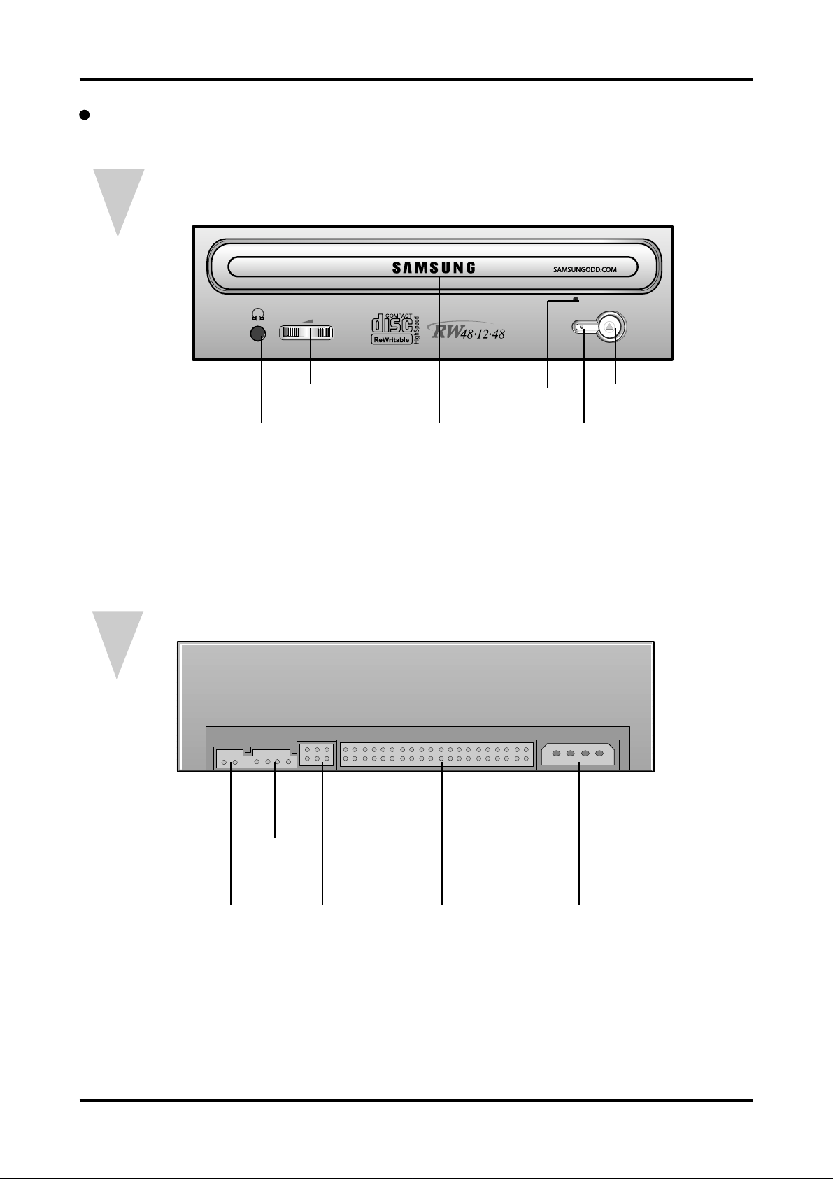
3
1. Front
2. Rear
Digital
output terminal
(Optional)
Sound
output terminal
Master/Slave
select pin
Interface
terminal
Power terminal
External Part Name
Earphhone jack
Stop/Open
button
Emergency
HOLE
Up/Down
Volume
LEDDisc tray
Page 5
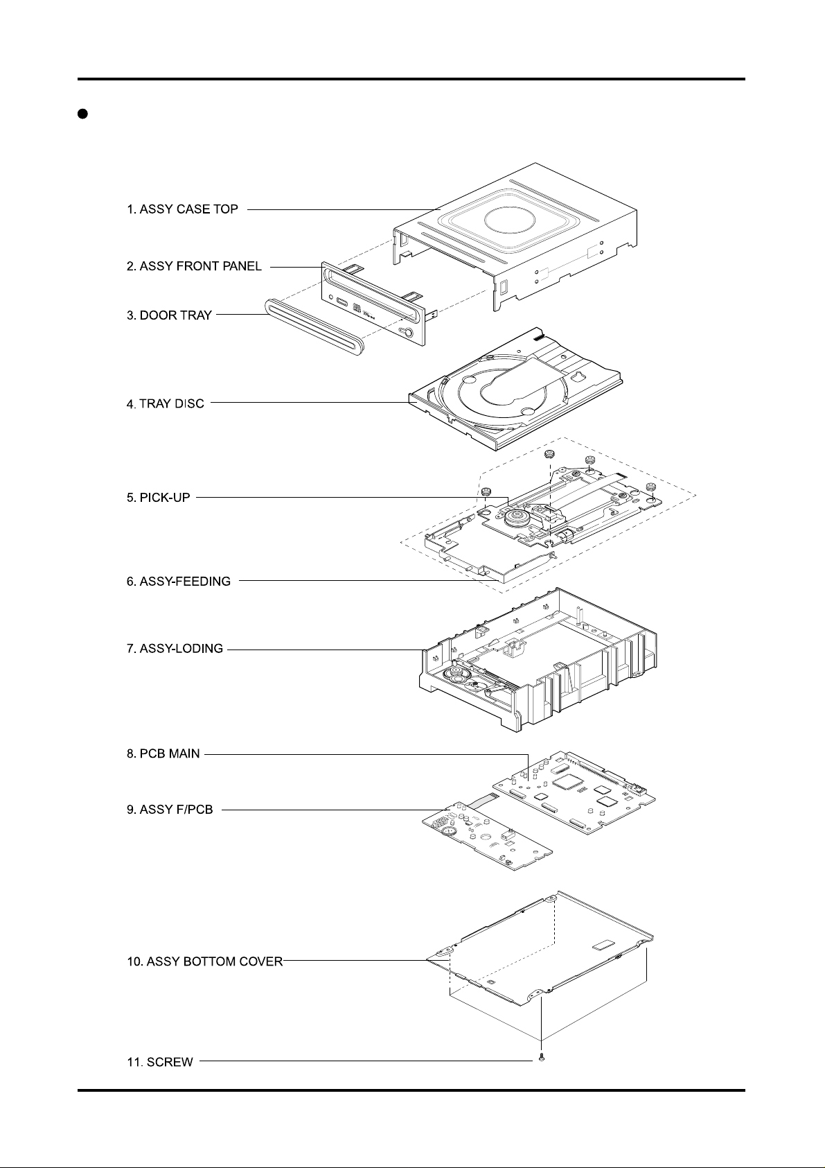
4
Disassembly Diagram
Page 6
5
Device Part List
PART NAME CODE No SPECFICATION
ASSY DECK BG97-02248A -
BG60-00009A 1.SCREW TITE M1.7*5(10)
LOADING BG97-02250A 1.ASSY LOADING -
BG61-00203A 1.MAIN FRAME HIPS(HG1760S)
BG66-00061A 2.GEAR TRAY POM(F20-03)
BG66-00032A 3.GEAR PULLEY POM(F20-03)
BG66-00044A 4.BELT PULLEY CR-70(BLK 1.3t)
BG97-00789A 5.ASSY LOADING M/T BG31-00027A - LOADING MOTOR RF-300CH-11440 ¿Ü
BG66-00033A - PULLEY MOTOR POM(F20-03)
BG66-00034A 6.LEVER EJECT POM(F20-03)
BG66-00062A 7.SLIDE CAM KOCETAL(K700)
TRAY DISC BG66-00060A 1.TRAY DISC ABS ( SR-0320D )
FEEDING BG97-02251A 1.ASSY FEEDING -
BG61-00078A 1.SUB CHASSIS ABS(GF20%)
BG73-00012A 2.RUBBER-INSULATOR BUTHYL 25Hs
BG73-00027A 3.RUBBER-INSULATOR BUTHYL 25Hs
BG61-00238A 4.MAIN BASE M SECC+POM
BG61-00237A - MAIN BASE P SECC 2.0T
BG31-00025A 5.ASSY STEP M/T “SPS-15RF-054K, P4.5mm”
BG61-00180A 6.GUIDE PU POM(NW-02)
BG61-00122A 7.SHAFT PU R “SUS420J2,¥õ3.0,L85.5mm”
BG31-00036A 8.MOTOR SPINDLE “RSM-2615A,DMBSPC75A”
- FFC-SPM 15 PIN
BG97-02247A 9. ASSY TURN TABLE BG59-00017A TURN TABLE ABS ADC12
BG63-00084A COVER T/T ABS SN PLATE T0.6
BG59-00018A TURN TABLE BALL “STEEL ¥Õ2.5,11EA”
BG73-00026A RUBBER-T/T ABS CR(NEO-B-6150)
BG59-00019A MAGNET T1.5
BG61-00018A BRKT-T/T SECC T1.0
BG30-00025A 10.PICK-UP SW-232B
BG41-00184A 11.EFFC PU “32 PIN (P0.5),88mm”
BG97-01729A 12.ASSY SLIDER STEP BG66-00052A - SLIDE STEP POM(NW-02)
BG61-00225A - SPRING STEP SUS 304-WPB
BG61-20031A 13.HOLDER CAM POM(M90-44)
AH60-10145A 14.SCREW TITE M1.7*5(5.5)
AC60-10074A 15.SCREW TITE M2.6*6
6001-001348 16.SCREW M1.7*3.5
6003-001260 17.SCREW TITE M1.7*4.0*3.5
BG69-00127A 18.PAD-DECK PORON LE-20 2T
BG73-00022A 19.RUBBER-DVA SILICON 25µµ
BG61-00178A 20.PLA-VIB/ABSORBER SECC 2T
ETC 3409-001138 -.SWITCH DETECTOR
BG63-00052A -.SHEET PU PVC FILM 0.85T
BG41-00182A -.FFC MAIN 13 PIN
- -.OIL EP-100
- -.GREASE KG-110
- -.GREASE G-754
Page 7
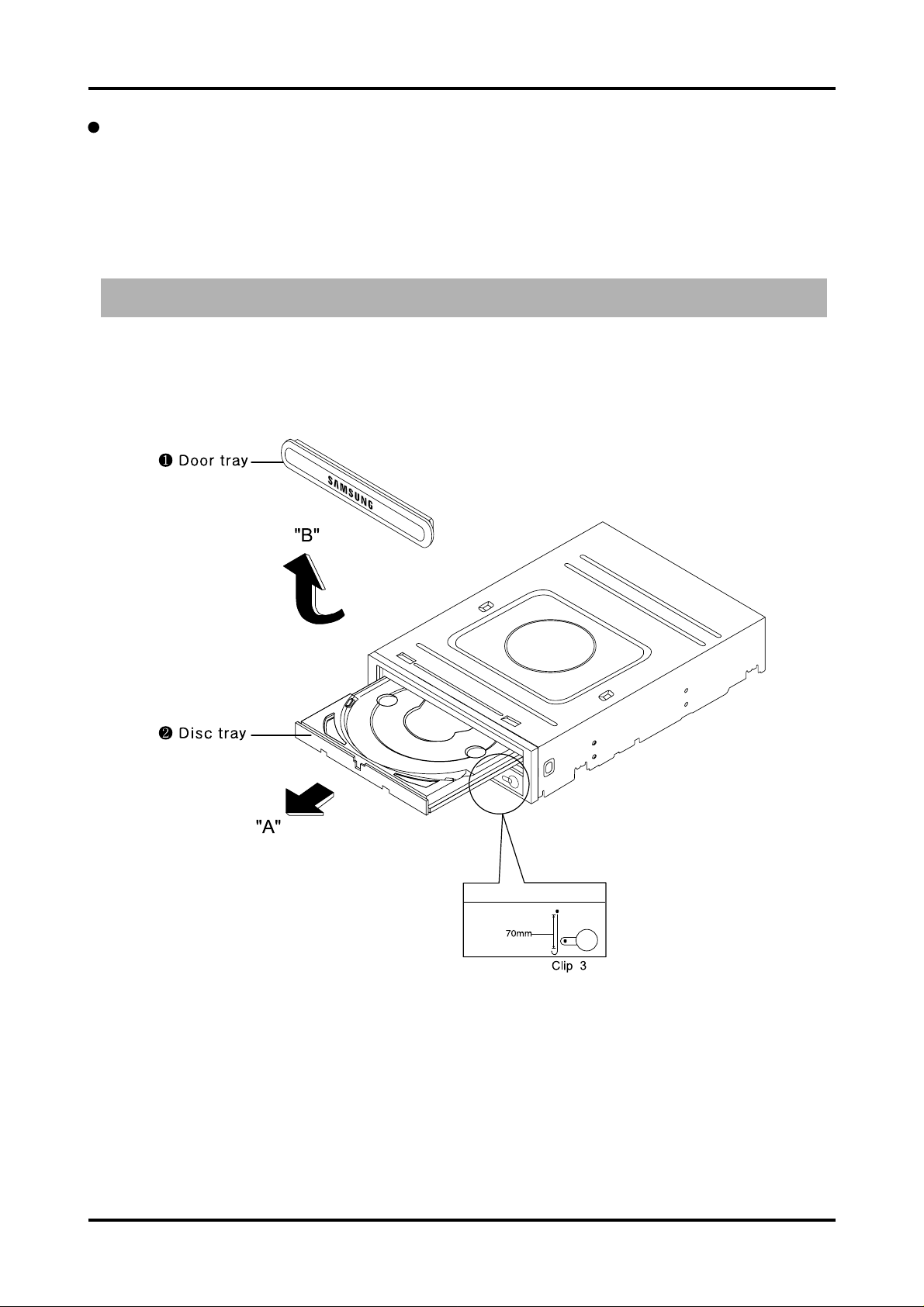
6
Disassembly and assembly
Door-tray
Exterior and PCB disassembly
Figure - Door-tray
1) Supply power to open the tray¶Êin direction of arrow “A”
2) Lift up the door¶Â in direction of arrow “B”
3) Close the tray¶Êand power off.
Reference : If the tray¶Êdoesn't open, push the clip3 into specified hole shown in detailed figure to open
it compulsorily.
Page 8
7
Disassembly and assembly
Panel-front
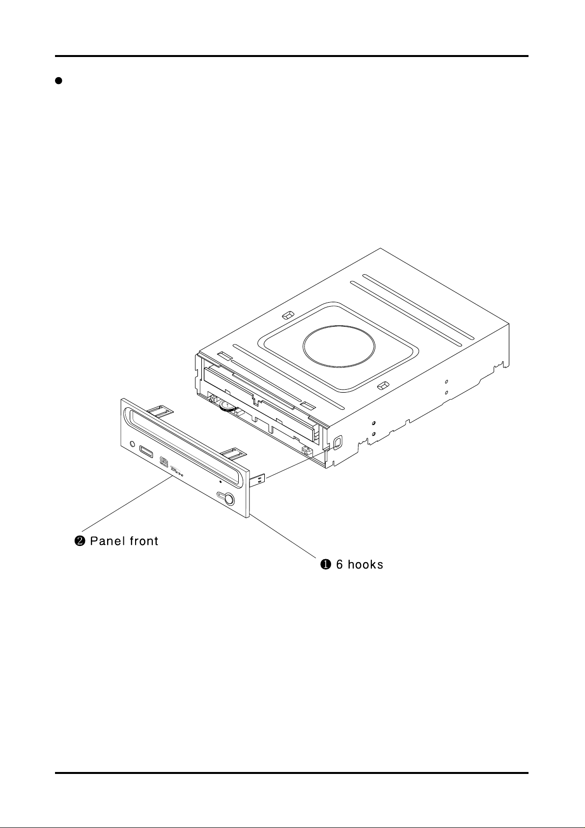
Exterior and PCB disassembly
1) Remove 6 hooks¶Â
2) Take out the panel-front¶Êforward.
Figure - Panel-front
Page 9

8
Disassembly and assembly
Top-cabinet
Exterior and PCB disassembly
Figure - Top-cabinet
1) Remove 4screws¶Â in the bottom
2) Lift up the top-cabinet ¶Ê
Page 10

9
Disassembly and assembly
Ass'y-frame Low
Exterior and PCB disassembly
Figure - Ass'y-frame Low
1) Lift up the ass’y frame¶Ê low
Page 11

10
Disassembly and assembly
MAIN-PCB
Exterior and PCB disassembly
Figure - Disassembly connector
1) Disassemble the PICK-UP FPC¶Â in PCB.
2) Disassemble the FFC¶Êbetween Main PCB and Front PCB.
3) Disassemble the FFC¶Ábetween Main PCB and Front PCB.
4) Push 2hooks¶Ëfor PCB fixing in deck.
5) Disassemble the MAIN-PCB
¶È
6) Remove soldering at motor connection wire¶ÍPCB.
7) Press 2hooks¶Îfor PCB fixing in deck and Disassemble the FRONT-PCB
Page 12

11
Disassembly and assembly
Tray
Deck disassembly
Figure - Tray
1) Push 2hooks¶Â.
2) Take out the Tray¶Êin direction of arrow.
Page 13

12
Disassembly and assembly
Ass’y-Deck
Deck disassembly
Figure - Ass’y-Deck
1) Move the slide cam¶Â in left direction.
2) Remove screws¶Ê.
3) Disassemble the Ass’y-feeding ¶Áin arrow “B” direction with pushing the 2hooks in direction of arrow “A”
Page 14

13
Packing Diagram and Part List
NO CODE-NO DESCRIPTION SPECIFICATION Q’TY
1 BG69-00146A MASTER CATON-BOX DM 3 1/8EA
2 BG69-00147A PACKING-CASE SW-224B/DOM SW-1 MANILA 240g 1EA
3 BG69-00034A CUSHION-SET EPS 2EA
4 BG69-30305A BAG-PE T0.05 2EA
5 BG46-00024A S-W UTILITY 1EA
6 BG68-00352A MANUAL USERS 1EA
7 BG95-50004A ASSY-SCREW 1EA
8 BG60-12001H SCREW-MACHINE M3 * 6 1EA
9 BG39-30002A BAG-PE 1EA
10 BG39-00010A CABLE-IF SR 380MM 1EA
11 BG39-42001B CABLE-WIRE HARNESS 4P, 3P, N, UL2547/UL1061 4EA
12 BG69-30307A BAG-PE T0.05 1EA
13 0203-001222 TAPE-MASKING PP-BEING 0.34M
14 BG68-00355A LABEL-RATING SW-224B/DOM, ART PAPER 1EA
15 BG68-50005A LABEL-QMS ART PAPER 1EA
16 BG68-00296C LABEL-BAR CODE DOM MODEL, ARTPAPER 1/8EA
17 BG68-00327A LABEL-BROKEN ART PAPER 1EA
ASS’Y
Page 15

14
Block Diagram
Page 16

15
Trouble Shooting
Check the power source and initial state.
Is electrity of 5V and 12V normally input
after the connecting the power cable ?
Y
Do RL3E804, RL5E935 oscillate ?
Y
Dose the voltage of the 1pin of IC502
change from 3.3V ?
Y
Is electricity of 2.5V normally
output from the 3pin of IC503?
Y
When you transfer the PICK-UP
to the outer cycle, and turn the power on,
dose it move to the inner one?
Y
TRAY IN / OUT ?
Y
Refer to ‘NO SLED operation’
Refer to ‘Check TRAY IN / OUT’
Refer to ‘check LASER DIODE ON’LASER DIODE ON ?
Check the connection of the
power short and cable.
If the power of RL3E804, RL5E935
is normal when you check,
replace X201, X301.
N
N
If the power of ICIC502 (3pin) is normal
when you check, replace IC502.
If the power of IC503 (2pin) 5V is normal
when you check, replace IC503.
N
N
N
N
N
Page 17

16
FOCUS UP / DOWN ?
Y
FOCUS LOCK ?
Y
DISC rotation ?
Y
SPINDLE LOCK ?
Y
AUDIO OUTPUT ?
Y
WRITING Normall ?
Refer to ‘ FOCUS LOCK ’
NN
N
N
N
Refer to ‘ NO DISC ROTATION ’
N
Refer to ‘ NO AUDIO OUTPUT ’
N
Refer to ‘ NO WRITING ’
N
Page 18

17
When you transfer the pick-up to the outer
cycle and turn the power on, dose the
pick-up move to the inner one ?
SLED operation of normal.
If the constant of IC301 and GND, pattern’s
when you check, replace.
Y
Y
N
N
If the constant of IC401 and GND,
pattern’s when you check, replace.
N
The below waveform is outputted in
IC301 1, 99pin ?
Y
Y
Replace stepping Motor.
Y
The below waveform is outputted in
IC401 35, 37pin ?
Y
No SLED OPERATION
Page 19

18
Is the connector properly
inserted into CN30 ?
Try the operation after inserting the
connector to CN3 properly.
Check the SW701 patterns and the
welding condition.Replace it if the
condition is normal.
Y
N
N
Check the SW701 Open and Close
patterns and the welding condition.
Replace it if the condition is normal.
N
Check the condition and patterns of
R409, R410.If they are normal,
replace IC401.
N
When pressing the EJECT SW,
does the IC401 Pin26 vary from 1.65V
to the value between 1.15V and 2.15V
and then show 0V finally?
N
Is the Tray Motor able to output the
Pin49 and 50 of IC401?
Replace TRAYMOTER.
Y
When pressing the EJECT SW,
does the peak value of the
IC301 3Pin become 3.3V?
Y
When it is in the Tray Open mode,
does the IC301 6Pin show 1.65V?
Y
When pressing the EJECT SW, does the
IC401 Pin26 vary from 0V to the value
between1.15V and 2.15V and then show
1.65V finally?
N
Y
Y
Y
No Tray open / close operation
OPEN
CLOSE
Page 20

19
Is the connector inserted normally
into the CN10?
Y
Isn’t there any problem
with the FPC Wire ?
Y
When the SLED is moved to the
inner circle, is electricity of about 1.65V
output from the 80pin of IC101 ?
Y
Is electricity of about 1.65V input
through 71pin of CN101 ?
Y
Replace PICK -UP.
No LASER DIODE ON
Try again after a normal insertion of the
connector into CN10.
N
Try again after replace of FPC Wire.
N
If the pattern of IC101 and sodering is
normal when you checked, replace IC301.
If the time transfer 71pin of IC101
and soldering are ok is when you checked
replace IC101
N
N
The value of voltage can be modified slightly, depending on the result of power calibration or the media.
Page 21

20
CH 2 : Focus Up / Down FE
CH 3 : S curve
CH 4 : Focus Servo On
If the power of IC101 and GND, soldering
is normal when you check, replace IC101.
If the power of IC201 and GND, soldering
is normal when you check, replace IC401.
If the power of IC201 and GND, constant
is normal when you check, replace IC201.
The below waveform(CH B) is
outputted in ICIC401 45, 46pin ?
FOCUS UP / DOWN ?
Dose the S-curve below come out of the
76(TP:FE)pin of IC101after insertion of a disc ?
Is the waveform above input
through the 128pin of IC201 ?
Y
Y
If the power of IC201 and GND, soldering
is normal when you check, replace IC201.
N
N
The below waveform(CH B) is
outputted in IC201 132pin ?
N
N
N
N
Y
1. Is the FPC Wire inserted normally
into the CN10?
2. Isn’t the FPC wire disconnected ?
Y
1. Try again after a normal insertion of the
connector into FPC Wire.
2. Try again after replace of FPC Wire.
Replace Pick-up.
Y
Y
No FOCUS LOCK
Page 22

21
If the power of IC201 and pattern’s,
soldering is normal when you check,
replace IC201.
Is the waveform below output
through 140pin of IC201 ?
YNY
Is the waveform above input
through 24pin of IC401 ?
Y
Does output but spindle Motor rotate ? Replace MOTOR.
Y
Y
N
If the power of IC401 and pattern’s,
soldering is normal when you check,
replace IC401.
N
NN
No SPINDLE MOTOR ROTATION
Page 23

Replay of AUDIO after
insertion of AUDIO DISC ?
Y
Is the audio output from the
164, 167pin of IC201 ?
If the power of IC401, GND, soldering is
normal when you check, replace IC200.
Y
Is the audio output from the
11, 13pin of CN30 ?
Y
Is the audio input from the JK701 ?
Y
Check the connection of the JK701 is and
normal when you checked, replace JK701.
No AUDIO OUTPUT
22
N
Replace FRONT PCB
N
Check the connection of the CN30 is and
normal when you checked, replace VR701.
N
Page 24

No WRITING
23
Can WLT216B.EXE be
executed properly?
When you try to write the records
again,does it work properly?
Was the Power Calibration
executed properly?
When writing the records,does the
voltage at the PIN 20 (XWGATE)
of CN10 decrease from 5V to 0V?
N
Check the condition of the
power at CN10,
GND and the welded part.
If they are normal, replace IC101.
N
N
Y
Y
Y
Replace P/UP or the entire MECHA.
N
Page 25

24
Circuit Diagram
Main
Page 26

25
Circuit Diagram
Front
 Loading...