

Samsung SPH-A900 Service Manual
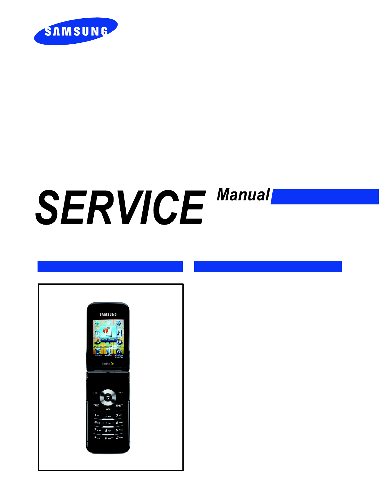
CDMA TELEPHONE
SPH-A900
CDMA TELEPHONE
CONTENTS
1. General Introduction
2. Circuit Description
3. Installation
4. NAM Programming
5. Product Support Tools
6. Test Procedure
7. Flow Chart of Troubleshooting
8. Exploded Views and Parts List
9. Block Diagram
10. Electrical Parts List
11. PCB Diagrams
This Service Manual is a property of Samsung Electronics Co.,Ltd.
Any unauthorized use of Manual can be punished under applicable
International and/or domestic law.
ⓒ
SamsungElectronicsCo.,Ltd. December.2005
Printed in Korea.
Code No.: GH68-08836A
BASIC.

1. General Introduction
1-1. General Instruction
The SPH-A900 enables mobile users to communicate 3G CDMA2000 1X service into a single handset.
For CDMA/PCS mode, The SPH-A900 supports Release A of the CDMA2000 1X standard.
The SPH-A900 also features EV-DO high-speed data, Bluetooth as well as a swiveling 1.3 megapixel
digital camera.
This stylish clamshell phone supports dual color displays, Bluetooth, MMS, voice dialing, airplane mode
and EV-DO services.
1-1
SAMSUNG Proprietary-Contents may change without notice
This Document can not be used without Samsung's authorization

General Introduction
1-2
SAMSUNG Proprietary-Contents may change without notice
This Document can not be used without Samsung's authorization

2. Circuit Description
2-1. Logic Section
2-1-1. Power Supply
Press "END" key to turn on the phone and then the
turns on the inner regulators(
The
V_BAT
MSM6500(UCP102) sends out PS_HOLD(logical HIGH) to keep the inner regulators on even after the
"END" key is released.
on/off by the TCXO_CTRL signal. The other regulators(
in the ON/OFF state by I
The regulated Voltage(u200, V_MSMCORE) are used in the core of MSM.
The regulated Voltage(u200, V_MSMC) are used in the digital part of MSM.
The regulated Voltage(u200, VPD) are used in the digital part and memory of MSM.
The regulated Voltage(u200, VPA) is used in the analog part of MSM.
The regulated Voltage(u200, V_RFTX) is used in the Tx RF part.
The regulated Voltage(u200, V_RFRX) is used in the Rx RF part.
The regulated Voltage(u200, V_TCXO) is used in the TCXO.
The regulated Voltage(u200, V_SYNTH) is used in the PLL part.
applied to ON_SW will change ON_SW_SENSE signal from HIGH to LOW.
V_MSMCORE, V_MSMC, VPD, VPA
V_RFRX
2
C-compatible 2 wire serial interface.
can be turned on/off by the RX_CTRL signal.
V_BAT
and
ON_SW
) of u200(MAX1526).
VDD2.6,V_SYNTH,V_RFTX,MOTOR_EN
signals will be connected. This
V_TCXO
canbeturned
)willbe
The regulated Voltage(u200, VDD2.6) is used in the voltage of camera .
The regulated Voltage(u200, MOTOR_EN) is used in the MOTOR.
2-1-2. Inner Charging Circuit Part
The most important function of the charger shall be done in the PMIC(Power Management Circuit u200).
When the phone with a battery is connected with a travel charging adapter, the inner charging circuit of
the PMIC(u200) will charge the battery by constant fast charge mode.
When battery reaches regulation voltage of 4.2V (default charging voltage for Li+mode), the charge
current drops quickly to 0mA
- Input voltage range : 4.25~6.5V
- Charging Temperature : 0°C~40°C
- Charging Method : Constant Voltage/Current -Charging Current : Normal 550mA
- Charging Time : Standard (800mAh) 2.5 ~ 3 Hrs
-ChargingMode:①Charging
②
Completion
2-1
SAMSUNG Proprietary-Contents may change without notice
This Document can not be used without Samsung's authorization

Circuit Description
- Charging Battery Regulation Voltage
①
Min 4.158V, Typical 4.2V, Max 4.242V(at TA:0°Cto+85°C)
②
Min 4.137V, Typical 4.2V, Max 4.263V(at T
:-40°Cto+85°C)
A
Universal Serial Bus Interface
SPH-A900 supports a Universal Serial Bus(USB) interface by the MSM6500, to provide an efficient
interconnection between the mobile phone and a Personal Computer(PC).
The MSM6500's USB interface is designed to comply with the Universal Serial Bus Specification,
Revision 2.0. An external USB transceiver(u200) is required to implement the USB interface.
2-1-3. Logic Part
The logic part consists of MSM, MEMORY,EL Keypad, LCD, CAMERA and other input and output
peripherals.
MOBILE SYSTEM MODEM(ucp102:MSM6500)
Industry standard ARM926EJ-S microprocessor is embedded. The MSM6500 chipset integrates
CDMA2000 1x and 1xEVDO service. The 1xEVDO solution can support High-speed peak data rates of
2.4Mbps on forward link and 153kbps on reverse link.
The MSM6500 device is offered in a 409 ball, 0.5mm pitch, CSP production package. Subsystems within
the MSM6500 device include a CDMA processor, a QDSP for voice compression, an ARM9TDMI
microprocessor.AlsointegratedintheMSM6500device are analog functions such as an audio voice
codec, PLL, transmit DAC
,ADCS, memories, USB controller, peripheral interfaces, and an enhanced
S
clock. It is one of the most important components of the CDMA cellular phone.
The interface circuitry consists of reset circuit, dual address/data bus and memory controls. The TCXO
clock of 19.2Mhz is used as the main clock of SPH-A900 model.
MCP : NAND FLASH and SDRAM (UME100(KBE00F003A))
MCP is consist of two 512Mbit(64M*8) NAND FLASH and two 256Mbit(4M*16*4Banks) Mobile SDRAM.
NAND FLASH is used to store the Font data and program. EFS area is used to store ESN, NAM
information, telephone directory, SMS messages and other important information of the phone, and also
to store application programs and downloaded stuffs such as BREW applications and MP3. MCP is also
used to excute the DMSS(Dual Mode Subscriber system) software.
Using the down-loading program, the program can be changed even after the terminal is fully assembled.
2-2
SAMSUNG Proprietary-Contents may change without notice
This Document can not be used without Samsung's authorization

Circuit Description
EL Keypad
For key recognition, key matrix is operated by using SCAN(0:6) and KEYSENCE(0:3) of the input ports
of MSM. EL(Electro Luminescence) is included in the keypad for easy operation in the dark.
LCD Module
LCD is composed of a Transmissive with Micro Reflective(TMR) type Main TFT-LCD Panel, Transflective
type Sub TFT-LCD Panel, a driver circuit and a back-light unit.
The resolution of a 2.22" Main LCD contains 240 * 320 pixels, the resolution of a 1.07" Sub
LCD(Transflective) contains 96 * 96 pixels.
Clock
CPU clock : 19.2MHz. Clock signal from the TCXO
Sleep clock : 32.768KHz. Clock signal for sleep.
TCXO/N : 19.2/N MHz. This clock source is used by various blocks of the MSM6500 device, such
as the ARM9CORE, UARTs, general-purpose PDMs and TCXO is also used by the
MSM6500 device to produce CHIPX8.
USB clock : 48MHz. Clock signal for the USB interface
CAMERA
The camera module consists of 1/4 CIS type 1.3 Mega (1310K) Pixels CMOS sensor. The camera
module provides Auto IRIS, and Auto White-Balance functionality.
Bluetooth module
TM
Bluetooth module is a Bluetooth
1.1 and 1.2 compliant, stand-alone baseband processor with an
integrated 2.4GHz transceiver. Bluetooth module supports any voice and/or data application that requires
the Bluetooth SIG standard Host Controller Interface (HCI) via UART and PCM audio interfaces.
Operation Clock: 26MHz
Low-Power Clock: 32.768KHz
SAMSUNG Proprietary-Contents may change without notice
This Document can not be used without Samsung's authorization
2-3

Circuit Description
2-1-4. RF Interface Part
CDMA Data Interface
- TX_Q_P, TX_Q_N, TX_I_P, TX_I_N (U402) : Tx analog signal used during CDMA
- RX_I_P, RX_Q_P, RX_I_N, RX_Q_N (U301) : RX analog signal used during CDMA
RF Interface
- TX : TX_AGC_ADJ(ucp102) is used to control the TX power,
PA_ON_PCS(ucp102) is used to control the PCS power amplifier and
PA_ON_CELL(ucp102) is used to control the CDMA power amplifier.
- RX : TRK_LO_ADJ(ucp102) is used to adjust the TCXO module.
2-1-5. Audio Part
The MSM6500 device integrates a stereo wideband voice/audio CODEC into the Mobile Station Modem.
The integrated CODEC contains all of the required conversion and amplification stages for the
audio front end.
The CODEC operates as a 13bit linear CODEC with the transmit(TX) and receive(RX) filters designed
to meet ITU-T G.712 requirements. The CODEC contains the software controlled amplifier for both the
receiving and transmitting sections. Also, the vocoding schemes used will be 13kbps QCELP and 8Kbps
EVRC. The QCELP vocoder is based in the MSM internally.
2-1-6. Tx Audio Path
The voice signal from the microphone is filtered and amplified by the internal OP-AMP and is converted
to PCM data by the internal CODEC in the MSM. And then these signals are applied to the the
MSM(ucp102)'s internal vocoder.
2-1-7. Rx Audio Path
The PCM data from the MSM(ucp102) is inputted to the internal CODEC and the data will be decoded
by the internal DAC. Audio levels are adjusted by the amplifier. And then audio is sent to the receiver.
2-4
SAMSUNG Proprietary-Contents may change without notice
This Document can not be used without Samsung's authorization

Circuit Description
2-1-8. Speaker Path
When the MSM(ucp102) receives the data, its internal CMX generates bell and melody. The CMX bell
and melody generated in MSM6500 are sent to SAPA1D2.
The SAPA1D2 (stereo class - D audio power amplifier) is a high quality audio power conversion chip
generating 2.5W RMS output directly from the V_BAT supply. It is a high efficiency audio amplifier for
mobile applications. The gain of amplifier in SPH-A900 set to 4(V/V) . The output generated in SAPA1D2
is intended to drive two speakers.
2-1-9. Key Tone Generator
The CODEC data out from the MSM6500 is converted to DTMF signal by TONE generator of internal
CODEC, which is then amplified by the internal audio amplifier to be sent to the speaker units.
2-2. PCS Section
2-2-1. Receiver
LOW NOISE AMPLIFIER (U300)
The low noise amplifier(It is included in RFL6000 : U300) amplifies a weak signal received from the base
station to obtain the optimum signal level.
RF BAND PASS FILTER (F300)
The RF BPF(F300) passes only a specific frequency(1960±30 MHz) from the signal received from the
mobile station. The bandwidth is 60 MHz.
VOLTAGE CONTROLLED OSCILLATOR(VCO300)
The VCO(VCO300) generates the signal having 1715 ~ 1788MHz frequency range.
The VCO's output frequency is changed by control voltage. The PLL in S1M8690X generates this control
signal and this signal is changed into DC control voltage by R-C Loop filter.
2-5
SAMSUNG Proprietary-Contents may change without notice
This Document can not be used without Samsung's authorization

Circuit Description
Frequency Synthesizer Circuit
The PLL(Phased Locked Loop) block consists of VC-TCXO(TCK301), PLL in S1M8690X and
VCO(VCO300). Input reference frequency is generated at VC-TCXO(TCK301) and the RF local signal is
generated at VCO. PLL compares the two signals and generates the desired signal with a
preprogrammed counter which controls voltage.
VOLTAGE CONTROLLED TEMPERATURE COMPENSATED CRYSTAL OSCILLATOR (TCK301)
The VC-TCXO (TCK301) is a reference source of the frequency synthesizer. It provides 19.2MHz
reference frequency to PLL-IC. It is a voltage controlled temperature compensated crystal
oscillator having 19.2MHz ±2.5ppm frequency stability over all useful temperature range.
A correct frequency tuning is made by the control voltage.
2-2-2. Transmitter
Intenna
Intenna sends signal to the base station and receives the signal from the base station.
It is a tri-band Intenna and covers PCS band, CDMA band and GPS band.
RF Switch
It(U401:TQP4M3018) is used to switch the PCS path and CDMA path and the GPS
path. The RF signal passes through PCS path when PCS_MODE is high(2.6V). The RF signal
passes through CDMA path when CELL_MODE is high(2.6V). The RF signal passes through
GPS path when GPS_MODE is high(2.6V). PCS_MODE, CELL_MODE and GPS_MODE are
digital signals from MSM6500 GPIO.
Duplexer
Duplexer(DUF400) allows to transmit only the signals within acceptable Tx frequency range
(1880 ± 30 MHz) through the Intenna.
It provides the appropriate attenuation of transmitted signal at the receiver input and the appropriate
rejection of the transmit-generated noise in the Receiver band.
Power Amp
Power amplifier module(PAM400:WS1413) amplifiers signal to be sent to the base station
through the antenna.
2-6
SAMSUNG Proprietary-Contents may change without notice
This Document can not be used without Samsung's authorization

Circuit Description
Driver Amp
The driver amp(U402 ; included in S1M8690X) allows the signal to be inputted to the power
amp(PAM400) as a specified level.
Up-converter(Mixer)
The up-converter(U402 ; also included in S1M8690X) receives the local signal
and signal controlled by TX AGC amp(in S1M8690X) to generate Tx RF signal 1880±30MHz
which signal comes out from the mixer output by adding
F
means TX RF signal Frequency.
Tx
Automatic Gain Control Amp
The TX IF AGC amp (in S1M8690X) controls gain of AGC to deliver power level needed at
driver amp. Its control voltage varies from 0.2V to 2.5V.
FTx* 0.7999
FTx* 0.7999
local signal.
2-3. CDMA Section
2-3-1. Receiver
Low Noise Amplifier(LNA)
The low noise amplifier(It is included RFL6000 : U300) amplifies a weak signal received from
the base station to obtain the optimum signal level.
RF Band Pass Filter(Rx RF SAW Filter)
The RF BPF in F300 passes only a specific frequency(881.49±12.5 MHz) from the signal
received from the mobile station. The b andwidth is 25 MHz.
Voltage Controlled Oscillator
The VCO(VCO300) generates the signal having 1715 ~ 1788MHz frequency range.
The VCO's output frequency is changed by control voltage. The PLL in S1M8690X generates this control
signal and this signal is changed into DC control voltage by R-C Loop filter.
SAMSUNG Proprietary-Contents may change without notice
This Document can not be used without Samsung's authorization
2-7

Circuit Description
Frequency Synthesizer Circuit
The PLL(Phased Locked Loop) block consists of VC-TCXO(TCK301), PLL in S1M8690X and
VCO(VCO300). Input reference frequency is generated at VC-TCXO(TCK301) and the RF
local signal is generated at VCO. PLL compares the two signals and generates the desired
signal with a preprogrammed counter which controls voltage.
VC-TCXO
The VC-TCXO (TCK301) is a reference source of the frequency synthesizer. It provides 19.2MHz
reference frequency to PLL-IC. It is a voltage controlled temperature compensated crystal
oscillator having 19.2MHz ±2.5ppm frequency stability over all useful temperature range.
A correct frequency tuning is made by the control voltage.
2-3-2. Transmitter
Intenna
Intenna sends signal to the base station and receives the signal from the base station.
It is a tri-band Intenna and covers PCS band, CDMA band and GPS band.
RF Switch
It(U401:TQP4M3018) is used to switch the PCS path and CDMA path and the GPS
path. The RF signal passes through PCS path when PCS_MODE is high(2.6V). The RF signal
passes through CDMA path when CELL_MODE is high(2.6V). The RF signal passes through
GPS path when GPS_MODE is high(2.6V). PCS_MODE, CELL_MODE and GPS_MODE are
digital signals from MSM6500 GPIO.
Duplexer
Duplexer(DUF402) passes the RF signal of Rx frequency range(881.49 ±12.5 MHz) and Tx frequency
range
(836.49 ±12.5 MHz). It provides appropriate attenuation of transmitted signal at the receiver input and
appropriate rejection of the transmit-generated noise in the Receiver band.
It also matches LNA input in receiving part and PAM(PAM400:WS1102) output in transmitting part with
the Intenna.
2-8
SAMSUNG Proprietary-Contents may change without notice
This Document can not be used without Samsung's authorization

Circuit Description
Power Amp
Power amplifier module(PAM400:WS1102 amplifiers signal to be sent to the base station
through the antenna.
RF Band Pass Filter(Tx RF SAW Filter)
The RF BPF(F403) passes only specific frequency(836.49 ±12.5MHz) to send it to power
amp(PAM400:WS1102).
Driver Amp
The driver amp(U402 ; It is included in S1M8690X) allows the signal to be inputted to the
power amp(PAM400) as a specified level.
Up-Converter(Mixer)
The up-converter(U402 ; It is also included in S1M8690X) receives the local signal
FTx* 1.6666
and the signal controlled by TX AGC amp(in S1M8690X) to generate Tx RF signal
836.49±12.5MHz signal comes out from the mixer output by adding
F
means TX RF signal Frequency.
Tx
FTx* 1.6666
local signal.
Automatic Gain Control Amp
The TX IF AGC amp in S1M8690X controls gain of AGC to deliver power level to be needed
at Driver amp. Its control voltage varies from 0.2V to 2.5V.
2-9
SAMSUNG Proprietary-Contents may change without notice
This Document can not be used without Samsung's authorization

Circuit Description
2-4. GPS Section
Intenna
Intenna receives a signal from GPS satellites.
It is a tri-band Intenna and covers PCS band, CDMA band and GPS band.
RF Switch
It(U401:TQP4M3018) is used to switch the PCS path and CDMA path and the GPS
path. The RF signal passes through PCS path when PCS_MODE is high(2.6V). The RF signal
passes through CDMA path when CELL_MODE is high(2.6V). The RF signal passes through
GPS path when GPS_MODE is high(2.6V). PCS_MODE, CELL_MODE and GPS_MODE are
digital signals from MSM6500 GPIO.
Low Noise Amplifier Module(LNA)
The low noise amplifier(U302:ALM1106) amplifies a weak signal received from artificial satellite to
obtain the optimum signal level.
RF Band Pass Filter(Rx RF SAW Filter)
The RF BPF(U404:B9000) passes only a specific frequency(1575.42±1MHz) from the signal received
from the satellite. The bandwidth is 2 MHz.
2-10
SAMSUNG Proprietary-Contents may change without notice
This Document can not be used without Samsung's authorization

3. Installation
3-1 Installing and Removing the Battery
To install
battery into the phone. Put on the battery cover.
Make sure the cover on the back are inserted into
the matching slots in the phone. Press down until
the latchsnaps into place.
, open the battery cover and insert the
Specifications using TA (Travel Adapter)
Battery Type
Charging < 3 hours
SEC Code
To remove
battery cover latch release up completely. Pull and
lift the battery away from the phone.
Standard Battery
(Li-ion, 800mAh)
GH43-02101A
, make sure the power is off. Push the
3-1
SAMSUNG Proprietary-Contents may change without notice
This Document can not be used without Samsung's authorization

Installation
3-2
SAMSUNG Proprietary-Contents may change without notice
This Document can not be used without Samsung's authorization

4. NAM Programming
NAM program can be changed as following table:
Notes:
- In the NAM program mode, each item show you the currently stored data. you can modify the data
by entering a new data.
-Youcanmovetonextwindowbypressing"OK"key.
- When you press a wrong number, press "
"
BACK
You can move to menu screen by pressing "MENU" key.
-
" key to delete all number
- You can change some selection option keys by pressing "Left" or "Right" navigation.
4-1. Single NAM
4-1-1. General Setup
LCD Display Key in Funtion
Enter
##MSL#
SVC Menu
1: View
2: Edit
3: Done
Phone Number
1234567890
MSID
1234567890
SVC Menu
1: View
2: Edit
3: Done
Phone Number
1234567890
MSID
1234567890
SVC Menu
1: View
2: Edit
3: Done
##222222#
1ViewPhoneNumberandMSID
Right key or Down
key
MENU or BACK Mobile ID is displayed
2 Choose'Edit'tochangePhoneNumberandMSID
OK
OK
3 Choose 'Done' to exit the NAM mode
" key to delete the last number or press and hold
BACK
Enter the NAM Mode. Enter random 6-digit code (MSL) and
222222 is a default value.
Phone number is displayed
- Phone number setup
- To change phone number, enter phone #
-Storeit
- Mobile ID setup
- To change phone number, enter phone #
- Store it
4-1
SAMSUNG Proprietary-Contents may change without notice
This Document can not be used without Samsung's authorization

NAM Programming
4-1-2. NAM Mode Display
LCD Display Key in Funtion
#,#,3,2,8,2,# Enter the Data Program screen
3G Data Prog
1. User Name
2: Browser
3: IOTA Prog.
4: Camera URL
5: Advanced
6: Multimedia
7: Restore
Enter Service Code
??????
Advanced
1: View
2: Edit
ESN
B0000000
CERT
P_REV
6
VOCODER SVCOPT
EVRC
SCM
01101010
Lock Code
0016
Slot Mode
YES
Slot Index
2
HOME SID
4139
HOME NID
65535
MCC
310
MNC
00
ACCOLC
6
Right key or Down
Right key or Down
Right key or Down
Right key or Down
Right key or Down
Right key or Down
Right key or Down
Right key or Down
Right key or Down
Right key or Down
Right key or Down
Right key or Down
Right key or Down
5 Display the 3G Data program.
222222 Enter random 6-digit code (MSL) - 222222 is a default value
1 Choose "VIEW" to dispaly the Advanced NAM Information
key
key
key
key
key
key
key
key
key
key
key
key
key
Electronic Serial Number of the phone is displayed
Java security - Dormant Certificate Wakeup(On), and
Sleep(off) status is displayed
Common Air Interface version is displayed
13K or EVRC
Station Class Mark displays the power class,
transmission, slotted class, dual mode.
Lock code, current status is displayed
Slot mode. 'Yes' indicates the slot mode.
Slot mode index. The high number means longer
sleeping time
SID written in the list,current status is displayed.
NID written in the list,current status is displayed.
ImsI Mobile Country Code, current code is displayed.
ImsI Mobile Network Code, current code is displayed.
CDMA Access Overload Class, current status is displayed
4-2
SAMSUNG Proprietary-Contents may change without notice
This Document can not be used without Samsung's authorization

NAM Programming
NAM CDMA
Home Sys Reg
Yes
NAM CDMA
FSID Reg
Yes
NAM CDMA
FNID Reg
Yes
Right key or Down
Right key or Down
4-1-3. NAM Mode Setup
LCD Display Key in Funtion
3G Data Prog
1. User Name
2: Browser
3: IOTA P rog.
4: Camera URL
5: Advanced
6: Multimedia
7: Restore
Enter Service Code
??????
Advanced
1: View
2: Edit
ESN
B0000000
CERT
P_REV
6
VOCODER SVC OPT
EVRC
SCM
01101010
Lock Code
0016
Slot Mode
YES
Right key or Down
Right key or Down
Right key or Down
Right key or Down
Right key or Down
Left or Right key
key
key
MENU or BACK CDMA foreign NID,current status is displayed.
#,#,3,2,8,2,# Enter the Data Program screen ('##DATA')
5 Display the 3G dara program.
222222
2 Choose "EDIT" to change the Advanced NAM information
key
key
key
key
key
4-digit Code
OK
OK
CDMA Home system ID, current status is displayed
CDMA foreign SID, current status is displayed.
Enter random 6-digit code (MSL) - 222222 is a default
value
Electronic Serial Number of the phone is displayed
Java security - Dormant Certificate Wakeup(On), and
Sleep(off)
Common Air Interface version is displayed
Origination Service Option is displayed
-ChangeServiceOption
-Storeit
Station Class Mark displays the power class,
transmission, slotted class, dual mode.
Lock code, current status is displayed
- To change Lock Code, enter a new code
-Storeit
Slot mode. 'Yes' indicates the slot mode.
- Change status
-Storeit
4-3
SAMSUNG Proprietary-Contents may change without notice
This Document can not be used without Samsung's authorization
NAM Programming
Slot Index
2
HOME SID
4139
HOME NID
65535
MCC
310
MNC
00
ACCOLC
6
NAM CDMA
Home Sys Reg
Yes
NAM CDMA
FSID Reg
Yes
NAM CDMA
FNID Reg
Yes
0~7
OK
number
OK
number
OK
number
OK
number
OK
class number
OK
Left or Right key
OK
Left or Right key
OK
Left or Right key
OK
Slot mode index. The high number means longer sleeping
time
- To change Slot Index, enter new one
-Storeit
SID written in the list,current status is displayed.
- Enter new one to change code
-Storeit
NID written in the list,current status is displayed.
- Enter new one to change code
-Storeit
ImsI Mobile Country Code, current code is displayed.
- Enter new one to change code
-Storeit
ImsI Mobile Network Code, current code is displayed.
- Enter new one to change code
-Storeit
CDMA Access Overload Class, current status is displayed
- Enter new one to change code
-Storeit
CDMA Home system ID, current status is displayed
- Change status
-Storeit
CDMA foreign SID, current status is displayed.
- Change status
-Storeit
CDMA foreign NID,current status is displayed.
- Change status
-Storeit
4-4
SAMSUNG Proprietary-Contents may change without notice
This Document can not be used without Samsung's authorization
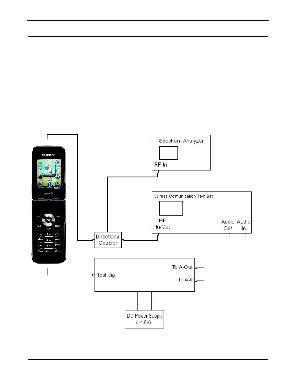
6. Test Procedure
6-1 List of Equipment
●
DC Power Supply
●
Test Jig
●
Test Cable
●
CDMA Mobile Station Test Set HP8285A, HP8960, CMD-80, etc
●
Spectrum Analyzer(include CDMA Test Mode) HP8596E,
6-2 Configuration of Test
6-1
SAMSUNG Proprietary-Contents may change without notice
This Document can not be used without Samsung's authorization
 Loading...