

Samsung SGH-Z320i Service Manual
UMTS TELEPHONE
SGH-Z320i
UMTS TELEPHONE
CONTENTS
1. Specification
2. Flow Chart of Troubleshooting
3. Exploded View and Parts List
4. MAIN Electrical Parts List
5. PCB Diagrams
6. Block Diagrams
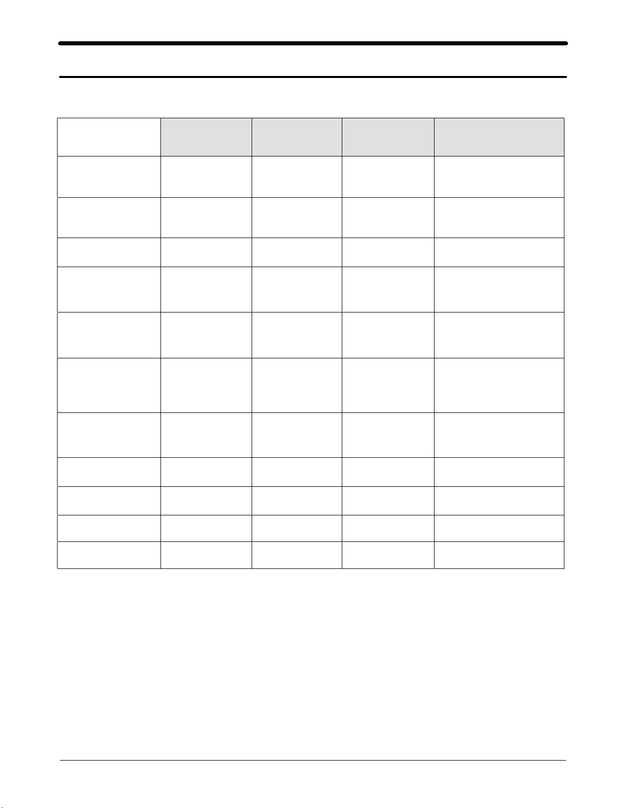
1. SGH-Z320i Specification
1-1. GSM/WCDMA General Specification
EGSM 900
Phase 2
Freq.
Band[MHz]
Uplink/Downlink
ARFCN range
Tx/Rx spacing 45MHz 95MHz 80MHz 190MHz
Mod. Bit rate/
Bit Period
Time Slot
Period/Frame
Period
Modulation 0.3GMSK 0.3GMSK 0.3GMSK
880~915
925~960
0~124 &
975~1023
270.833kbps
3.692us
576.9us
4.615ms
DCS1800
Phase 1
1710~1785
1805~1880
512~885 512~810 10562~10838
270.833kbps
3.692us
576.9us
4.615ms
PCS1900 WCDMA
1850~1910
1930~1990
270.833kbps
3.692us
576.9us
4.615ms
1920~1980
2110~2170
3.84Mcps/s
10ms
UL:2BPSk
DL:QPSK
MS Power 33dBm~5dBm 30dBm~0dBm 30dBm~0dBm
Power Class 5pcl ~ 19pcl 0pcl ~ 15pcl 0pcl ~ 15pcl CLASS3
Sensitivity -102dBm -100dBm -100dBm -106.7dBm
TDMA Mux 8 8 8 -
Cell Radius 35Km 2Km - -
MAX:24(+1,-3)dBm
MIN:<-50dBm
1-1
SAMSUNG Proprietary-Contents may change without notice
This Document can not be used without Samsung's authorization
SGH-Z320i Specification
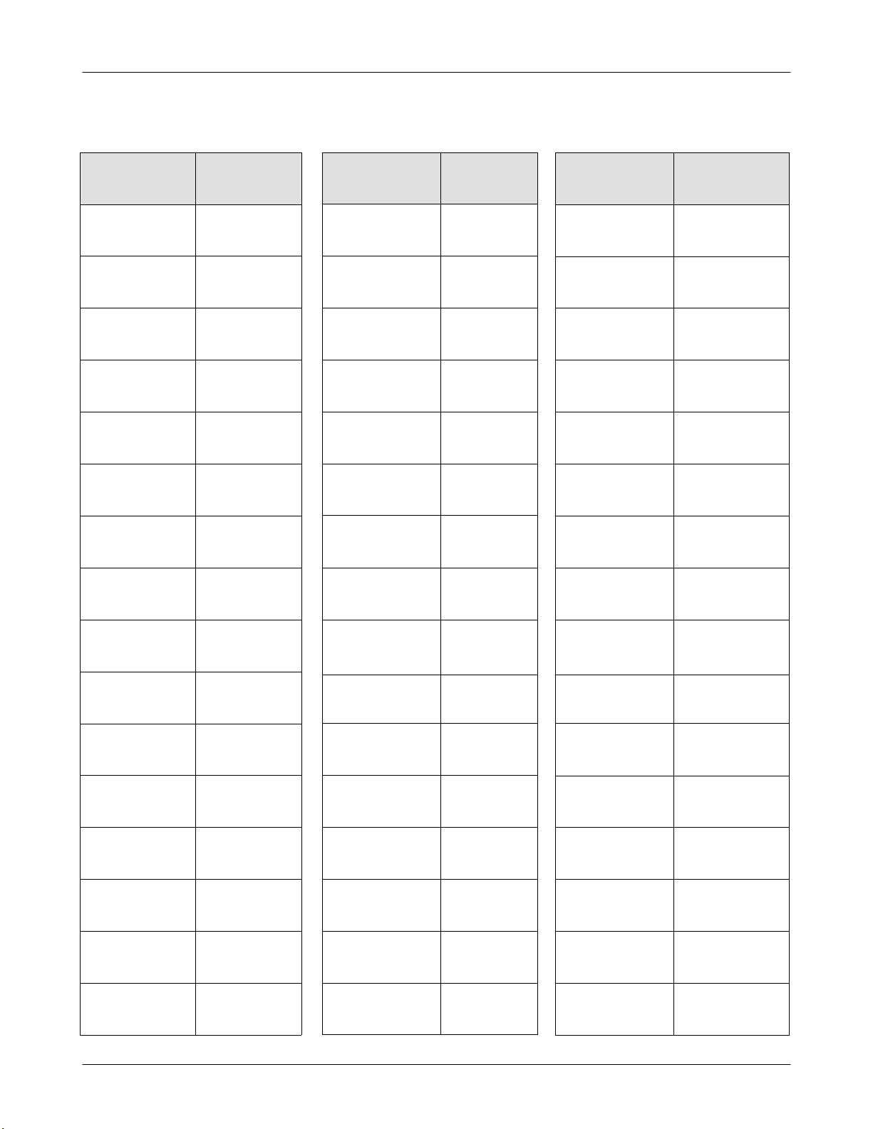
1-2. GSM TX power class
TX Power
control level
5 33±2 dBm
6 31±2 dBm
7 29±2 dBm
8 27±2 dBm
9 25±2 dBm
10 23±2 dBm
11 21±2 dBm
EGSM900
TX Power
control level
0 30±3 dBm
1 28±3 dBm
2 26±3 dBm
3 24±3 dBm
4 22±3 dBm
5 20±3 dBm
6 18±3 dBm
DCS1800
TX Power
control level
0 30±3 dBm
1 28±3 dBm
2 26±3 dBm
3 24±3 dBm
4 22±3 dBm
5 20±3 dBm
6 18±3 dBm
PCS1900
12 19±2 dBm
13 17±2 dBm
14 15±2 dBm
15 13±2 dBm
16 11±3 dBm
17 9± 3dBm
18 7±3 dBm
19 5±3 dBm
7 16±3 dBm
8 14±3 dBm
9 12±4 dBm
10 10±4 dBm
11 8±4 dBm
12 6±4 dBm
13 4±4 dBm
14 2±5 dBm
7 16±3 dBm
8 14±3 dBm
9 12±4 dBm
10 10±4 dBm
11 8±4 dBm
12 6±4 dBm
13 4±4 dBm
14 2±5 dBm
15 0±5 dBm
1-2
15 0±5 dBm
SAMSUNG Proprietary-Contents may change without notice
This Document can not be used without Samsung's authorization
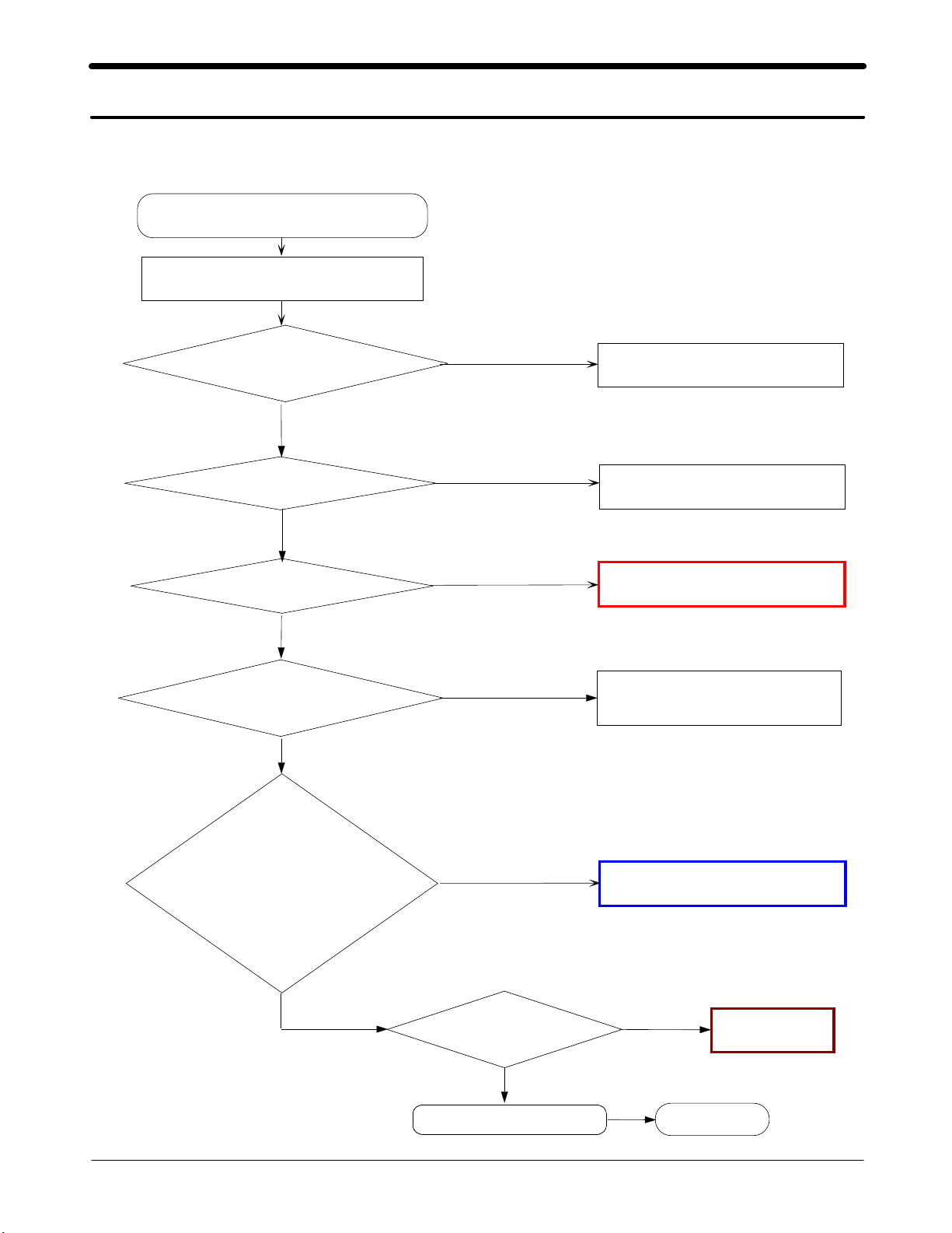
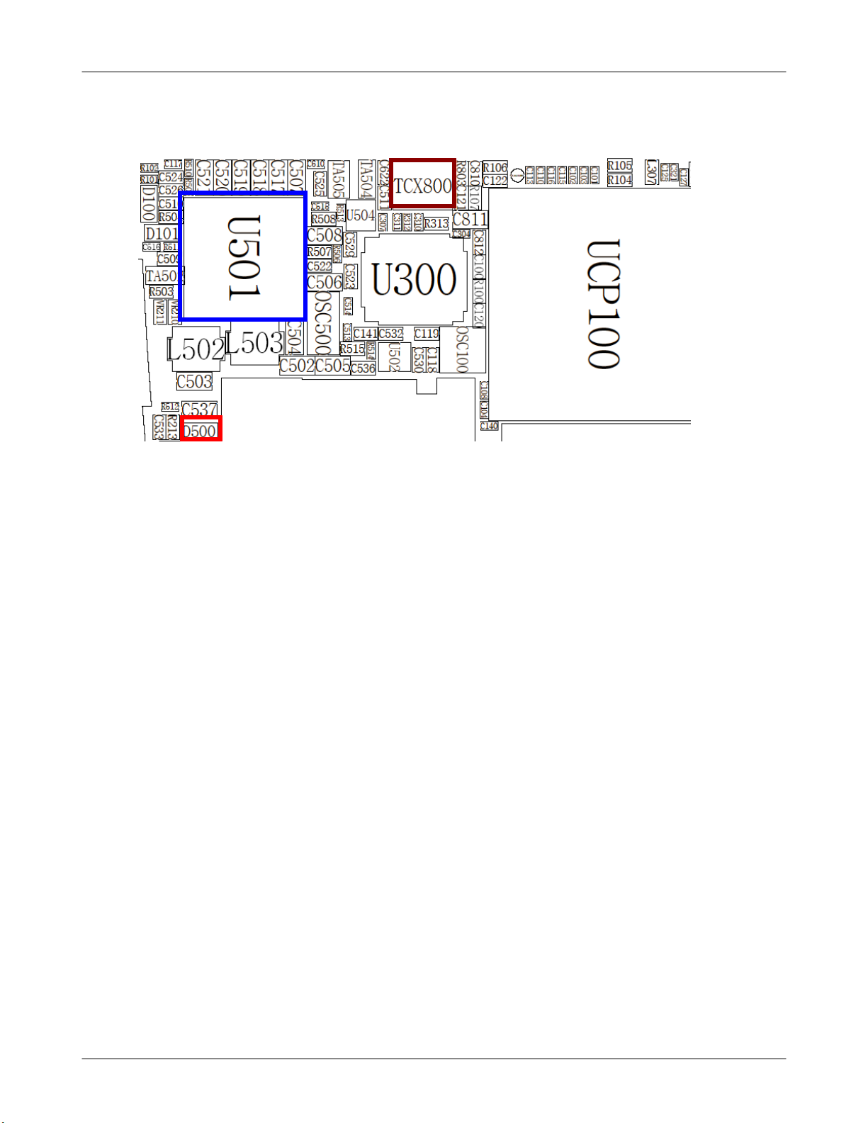
2. SGH-Z320i Flow Chart of Troubleshooting
2-1.Baseband
2-1-1. Power ON
'Power ON' Does not work
Check the current consumption
Current consumption
≥
100mA ?
YES
Check Voltage > 3.3V
YES
CheckD500isHigh
YES
The pin #3,5 of U501
≥
3.3V ?
YES
NO
NO
NO
NO
Download again
Charge the Battery
Check D500
Check the path of
D500 and U501
Check U501
pin #32≒1.2V ?
pin #36≒1.8V ?
NO
pin #50,56≒2.6V ?
pin #84≒2.85V ?
YES
U501 Check
Pin #53≒19.2MHz?
Vpp≥500mV?
YES
Check the initial operation
1
2-
SAMSUNG Proprietary-Contents may change without notice
This Document can not be used without Samsung's authorization
Check the U501
NO
check the TCX800
END
SGH-Z320i Flow Chart of Troubleshooting and Circuit Diagrams
V
0
.
3
_
T
B
V
6
.
2
_
A
M
S
M
V
6
.
2
_
P
M
S
M
V
0
.
3
_
M
I
S
U
V
5
8
.
2
_
C
I
M
V
8
.
1
_
E
M
S
M
V
2
.
1
_
C
M
S
M
7
0
5
C
8
0
5
C
6
0
5
C
5
0
5
C
4
0
5
C
2
0
5
C
3
0
5
C
2
3
0
0
5
5
L
L
9
0
5
C
0
7
1
7
2
4
1
1
V
V
5
5
_
_
G
W
E
S
R
V
V
1
0
5
U
S
U
B
V
G
_
H
B
S
C
U
V
6
2
1
N
I
_
V
9
6
2
8
1
3
2
3
3
3
3
2
E
E
B
C
A
A
C
C
P
S
P
M
M
M
M
M
_
_
U
S
S
S
S
M
_
G
W
_
M
M
M
M
E
G
S
_
_
_
_
G
R
E
V
G
E
G
W
W
V
R
E
E
R
S
S
V
R
V
R
V
V
V
V
N
N
N
_
_
_
P
L
L
T
T
U
T
E
M
P
C
K
C
F
N
_
_
_
I
_
T
C
_
S
S
G
O
B
T
A
A
N
N
S
H
C
A
B
B
S
S
U
V
V
I
B
V
I
C
0
5
8
6
7
5
3
4
6
1
4
5
0
5
R
V
5
8
.
2
_
O
X
C
T
V
5
8
.
2
_
T
N
Y
S
V
5
8
.
2
_
X
T
F
R
V
5
8
.
2
_
1
X
R
F
R
V
5
8
.
2
_
2
X
R
F
R
7
4
3
1
4
2
6
0
9
6
8
7
8
6
4
5
5
6
2
1
T
X
P
A
N
M
I
X
X
T
N
A
M
M
U
F
R
R
Y
L
S
S
R
F
F
R
S
W
M
M
_
_
_
R
R
_
_
_
_
_
G
G
G
G
G
G
E
E
G
G
E
E
E
E
R
E
E
R
R
R
R
R
V
V
R
R
V
V
V
V
V
V
K
T
T
L
U
P
N
U
C
N
O
Y
N
E
I
_
O
I
_
_
_
B
P
_
_
_
O
O
O
L
L
E
C
X
X
X
A
A
E
T
D
L
T
C
C
C
X
T
X
A
T
T
S
6
4
3
8
5
0
5
1
4
5
5
4
4
7
5
1
1
5
C
6
7
0
0
5
5
R
R
T
N
O
N
I
U
E
X
_
_
O
C
L
_
O
T
A
X
O
T
C
X
X
T
_
C
P
T
E
E
L
S
1
S
O
P
0
0
5
C
1
S
O
2
0
1
5
C
1
2
5
C
0
2
5
C
9
1
5
C
8
1
5
C
7
1
5
C
5
0
5
A
N
I
_
V
5
1
5
C
8
0
5
R
4
8
6
9
1
5
3
3
2
2
1
6
T
O
E
X
S
C
I
_
T
_
F
E
G
E
R
R
V
2
1
N
N
I
I
_
_
X
X
U
U
M
M
A
A
2
7
F
V
_
T
A
B
2
1
5
C
5
7
7
7
2
7
7
2
6
8
2
6
2
P
N
P
P
N
N
N
N
M
P
D
_
Y
N
V
B
G
R
_
_
D
F
F
_
E
E
H
R
R
S
L
F
T
N
U
T
_
O
E
U
_
O
O
X
_
_
U
F
B
E
S
M
A
R
U
0
3
2
8
1
8
9
0
0
1
5
5
R
R
F
T
E
U
R
O
_
_
3
X
C
I
U
M
M
P
A
2
G
E
N
4
1
5
C
M
_
_
_
_
_
_
Y
_
_
T
V
N
V
V
V
T
B
N
I
I
U
R
D
_
1
P
G
T
A
D
_
B
S
U
7
1
N
_
E
O
_
B
S
U
_
R
R
R
U
_
_
R
O
D
D
D
R
O
R
_
_
_
_
K
_
K
K
B
R
P
D
D
R
P
I
P
K
S
P
C
K
S
V
S
P
L
K
P
S
S
N
N
N
_
_
_
R
R
0
D
M
P
R
L
_
_
E
W
W
D
W
D
S
D
O
I
P
P
_
_
_
_
P
0
1
H
B
B
B
L
B
L
_
D
S
S
S
B
S
B
S
P
U
U
U
C
U
P
K
C
0
8
1
7
4
8
6
9
2
1
1
5
2
6
6
1
-
+
O
O
D
D
P
M
V
V
_
_
B
B
S
S
U
U
0
0
5
T
A
B
3
1
0
5
R
T
3
1
5
C
1
W
S
_
N
O
T
3
2
5
C
4
2
5
C
2
2
5
C
6
2
5
C
5
2
5
C
3
4
3
2
5
1
9
1
7
7
R
K
P
S
_
D
D
V
N
_
T
E
S
E
R
_
N
O
P
9
1
1
5
R
N
I
_
T
E
S
E
R
2
5
8
3
5
5
7
3
2
4
6
F
E
C
A
P
_
D
D
V
O
I
_
O
I
M
_
_
M
M
I
I
U
U
R
R
6
0
2
3
A
T
A
D
_
M
_
M
I
S
U
N
A
M
M
N
I
I
R
N
S
M
A
M
A
U
_
L
A
S
S
M
M
R
D
_
_
M
W
M
_
_
D
D
_
_
_
D
D
D
V
D
D
D
D
D
D
D
V
V
D
D
D
V
V
V
V
V
K
L
C
K
_
L
C
M
_
_
M
M
I
I
U
U
R
R
8
4
3
3
A
K
L
T
C
A
_
D
_
M
_
M
I
M
I
S
S
U
U
6
1
5
C
C
N
8
7
C
N
8
6
D
N
G
8
T
S
R
_
M
_
M
I
U
R
0
4
T
K
E
L
S
C
_
E
R
M
I
_
S
M
U
_
M
I
S
U
0
0
5
D
5
N
_
T
T
S
N
R
I
_
_
K
T
T
M
M
I
C
S
D
S
U
B
B
B
R
S
S
S
M
3
9
1
7
9
4
4
5
4
5
T
T
T
N
K
_
E
S
D
C
T
S
B
B
B
N
E
S
S
S
I
_
_
R
_
_
_
M
M
M
M
P
M
P
P
P
I
S
U
2
1
5
R
7
3
5
C
D
L
O
H
_
S
P
E
S
N
E
S
_
W
S
_
N
O
0
V
0
6
5
.
R
2
_
P
M
S
M
2
0
5
R
T
3
2
3
3
0
5
R
T
1
1
0
5
R
W
S
_
N
O
2
1
N
O
_
G
I
J
2
2-
SAMSUNG Proprietary-Contents may change without notice
This Document can not be used without Samsung's authorization
SGH-Z320i Flow Chart of Troubleshooting and Circuit Diagrams
3
2-
SAMSUNG Proprietary-Contents may change without notice
This Document can not be used without Samsung's authorization
SGH-Z320i Flow Chart of Troubleshooting and Circuit Diagrams
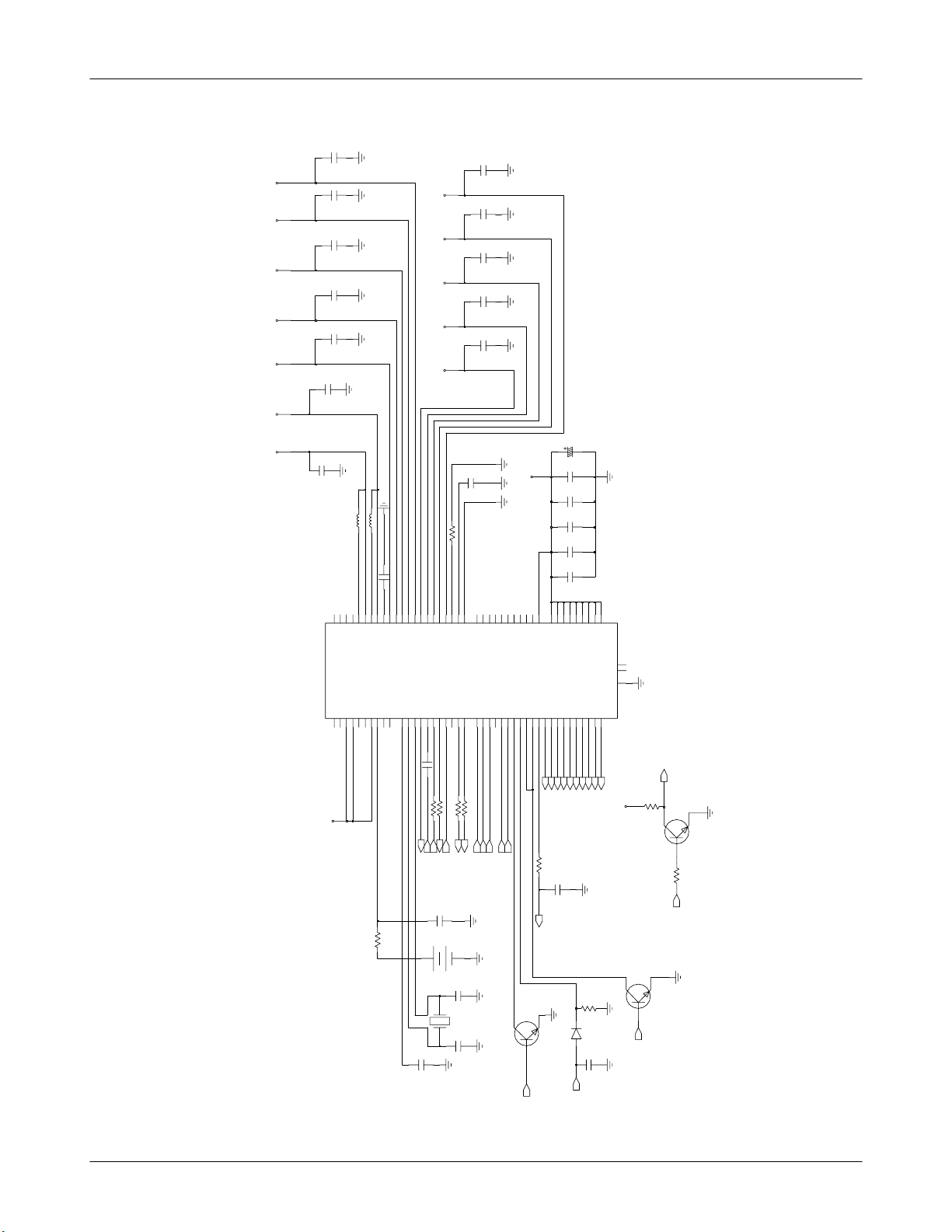
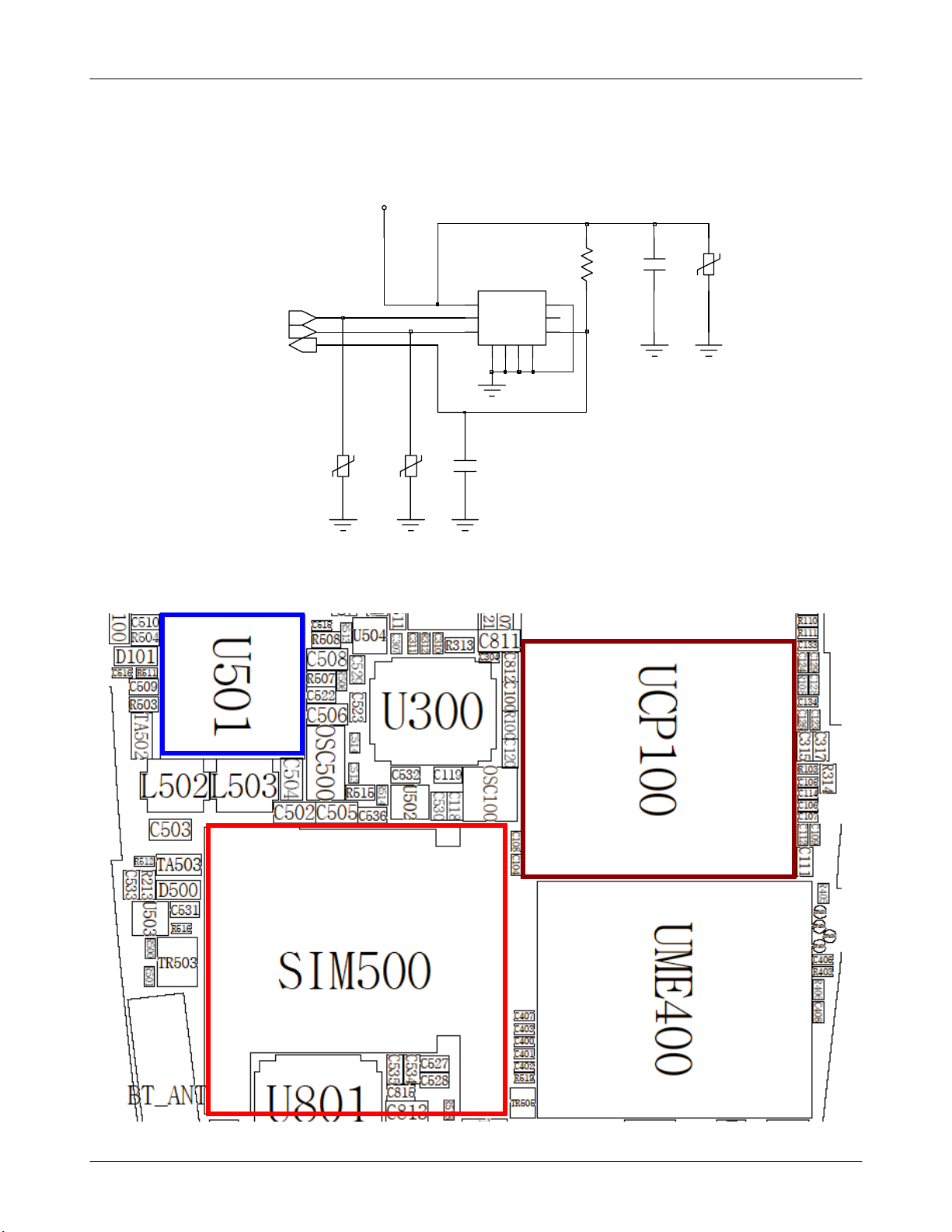
2-1-2. System Initial
Initial Failure
The pin #9 of U501
" Low --> High" ?
YES
Check the Sleep X-tal signal's
at C513 ?
YES
Check the clock signal's
at R507
YES
LCD Display OK ?
NO
NO
NO
NO
Check the U501
Check the OSC500
Check the clock generation
circuit (related to U501 and
TCX800)
Check the LCD part
YES
NO
Sound operation OK ?
YES
END
4
2-
SAMSUNG Proprietary-Contents may change without notice
This Document can not be used without Samsung's authorization
Check the Audio part
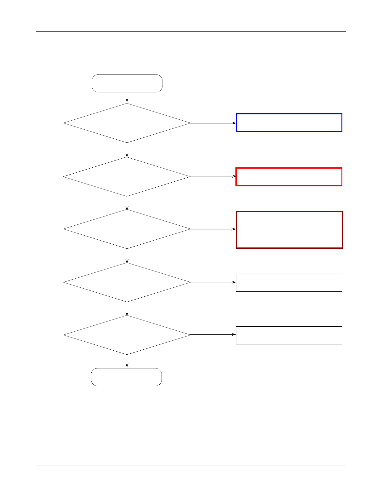
3. SIM Part
SGH-Z320i Flow Chart of Troubleshooting and Circuit Diagrams
"Please insert SIM card "
Check the SIM500's
Connection to SIM card
YES
Check the voltage
at SIM500 pin #1≒3.0V
YES
There is any signal
pin#2,#3,#4 of SIM500
YES
NO
Resolder or change SIM500
NO
Check the U501
NO
Check the U501 & UCP100
Check the SIM Card
END
** Check SIM's signal
when you see SIM checking display
5
2-
SAMSUNG Proprietary-Contents may change without notice
This Document can not be used without Samsung's authorization
SGH-Z320i Flow Chart of Troubleshooting and Circuit Diagrams
V
- Schmatic for SIM connection
USIM_3.0
USIM_RESET
USIM_CLK
USIM_DATA
VR501
- Layout for SIM connection
VR502
C536
SIM500
11
22
33 4
6
5
G
G
G78G
910
6
R515
5
4
C527
VR500
6
2-
SAMSUNG Proprietary-Contents may change without notice
This Document can not be used without Samsung's authorization
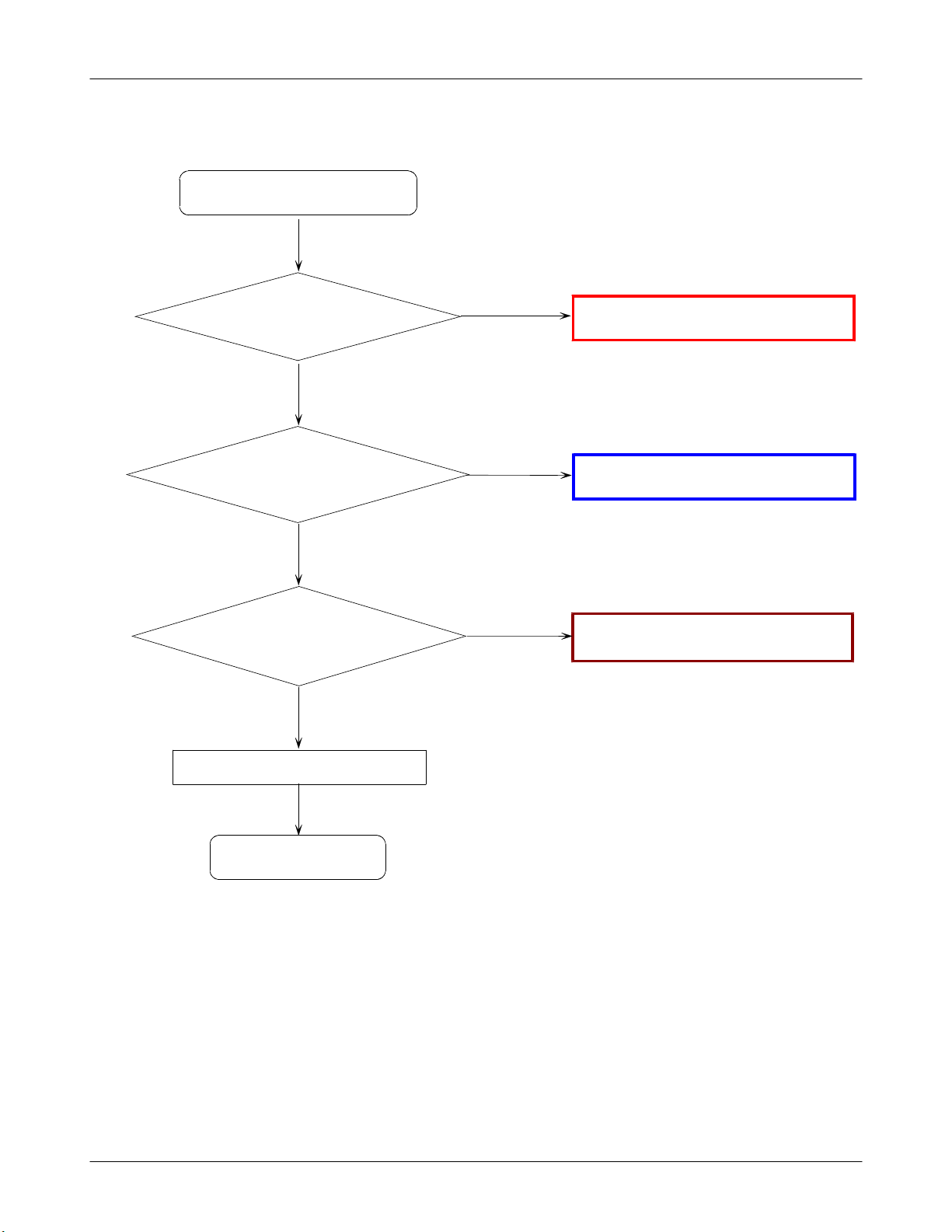
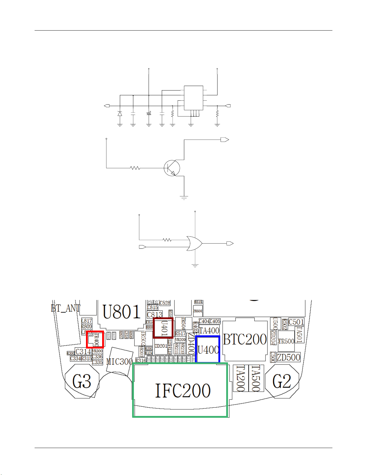
2-1-4. Charging Part
Abnormal charging operation
SGH-Z320i Flow Chart of Troubleshooting and Circuit Diagrams
Check IFC200's pin #20,21
is around 5V when charging
YES
Check TR400's pin#3
is "LOW" when charging
YES
Check U401's Pin #4
is "High" when charging
YES
NO
NO
NO
Check the TA
Check the TR400
Check the U401
Check U400's Pin #5
NO
is "LOW"
YES
END
7
2-
SAMSUNG Proprietary-Contents may change without notice
This Document can not be used without Samsung's authorization
Check the UCP100
SGH-Z320i Flow Chart of Troubleshooting and Circuit Diagrams
-SchmaticforCharging
VTA_5.0V
U400
ICHRG
ZD400
C404
TA400
C405
R402
1
VL
2
IN
3
GND
4
ISET
G
910GG1112
_CHG
BATT
_ACOK
G
_EN
8
7
6
5
VBAT
CHG_ON
R401
- Layout for charging
VTA_5.0V
R404
VTA_5.0V
JIG_ON_IF
CHG_DET
2
3
TR400
1
V_IN
R407
U401
5
1
VCC
B
4
Y
2
A
GND
3
JIG_ON
8
2-
SAMSUNG Proprietary-Contents may change without notice
This Document can not be used without Samsung's authorization
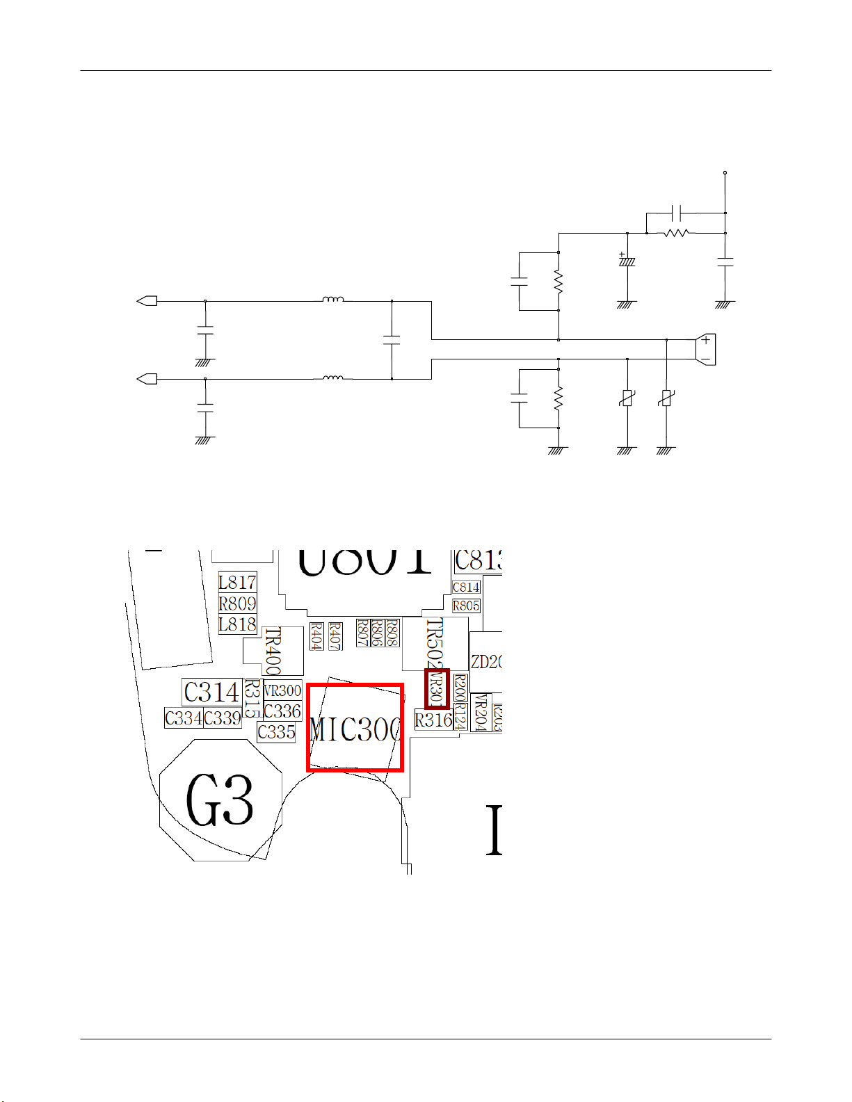
2-1-5. Microphone Part
Micro-phone does not work
SGH-Z320i Flow Chart of Troubleshooting and Circuit Diagrams
Is the assembled status of
Microphone O.K?
YES
Check the DC bias voltage on Mic path.
YES
The voltage of VR301 is
about 2.3V ?
YES
The microphone is OK
NO
NO
NO
Reassemble the microphone
Check the path around MIC
Bias circuit
Check UCP100
YES
END
9
2-
SAMSUNG Proprietary-Contents may change without notice
This Document can not be used without Samsung's authorization
SGH-Z320i Flow Chart of Troubleshooting and Circuit Diagrams
MIC_2.85V
C339
R315
MIC1P
MIC1N
C315
C317
L304
L305
C316
C335
C336
R316
R317
C314
1
0
0
0
3
3
R
R
V
V
C334
MIC300
10
2-
SAMSUNG Proprietary-Contents may change without notice
This Document can not be used without Samsung's authorization
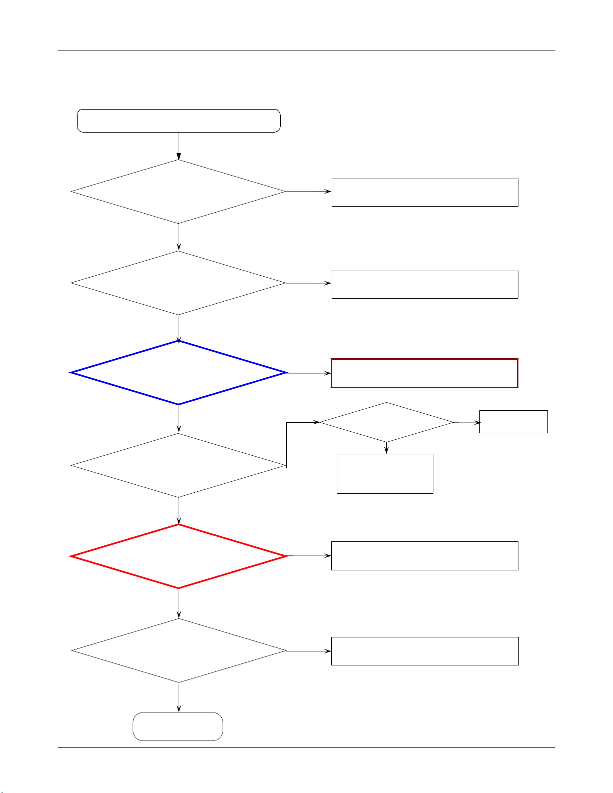
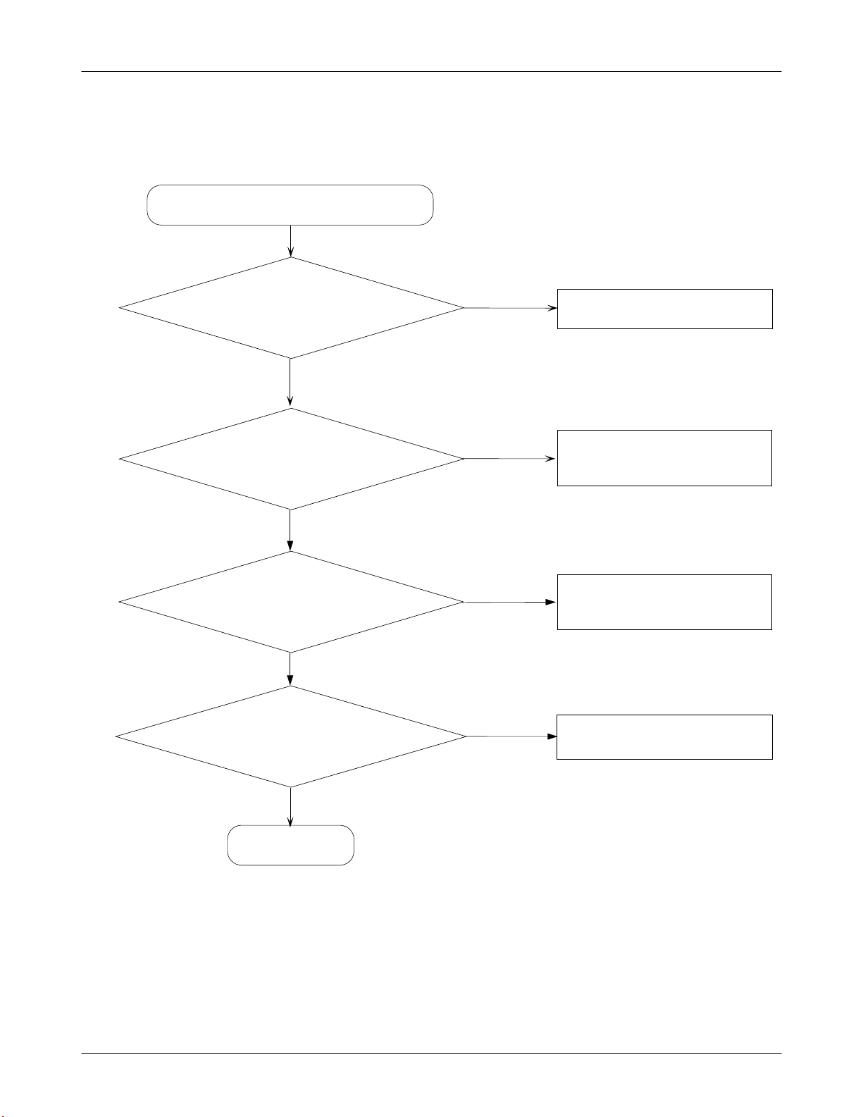
2-1-6. Speaker Part
There is no sound from speaker
SGH-Z320i Flow Chart of Troubleshooting and Circuit Diagrams
The terminal of Speaker
is OK ?
YES
There is signal
@ U301 pin #1
YES
There is signal
@U301pin#24
YES
The type of sound from the
Speaker is Melody
NO
NO
NO
NO
Replace the Speaker
Check the UCP100
Check the U302
SpeakPhone Mode?
YES
Check U302's
Pin #9,#13
NO
Receiver Part
YES
Thepin#32ofU300≒2.6V
The pin #7 of U300
2.8V ?
=
YES
Are there any signal in
pin #29 of U300
YES
END
SAMSUNG Proprietary-Contents may change without notice
This Document can not be used without Samsung's authorization
NO
NO
2-
Check the U501 & U502
Check the UCP100
11
SGH-Z320i Flow Chart of Troubleshooting and Circuit Diagrams
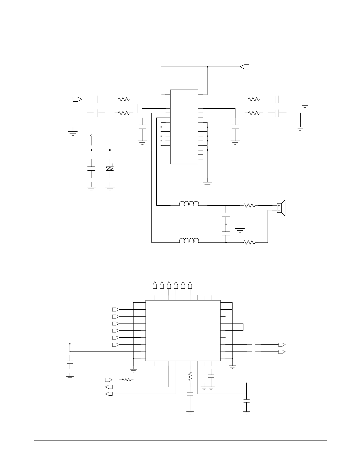
U301
ICE_AMP_L
C308
V_IN
C301
C302
C306
R301
R304
C332
1
EN_L
24
VIPL
22
VIML
23
VREFL
18
VOPL
16
VOML
3
VDD
7
VDD
9
VDD
15
VDD
19
VDD
21
VDD
EN_R
VIPR
VIMR
VREFR
VOPR
VOMR
VSS
VSS
VSS
VSS
VSS
VSS
GND
13
12
10
11
6
4
2
5
8
14
17
20
25
26
NC
27
NC
C333
AMP_EN
R302
R305
C300
C303
MSMP_2.6V
C304
NAND_D(1)
NAND_D(0)
NAND_WE
YMU_CS_N
YMU_A0
NAND_RE
33
26
27
28
29
30
31
32
34
25 24
G
D1
D0
/WR
/CS
A0
/RD
IOVDD
G
1
F302
C312
2
R
T
T
U
M
O
P
S
HPOUT-R
D
S
S
D
V
V
8
C313
1718
1
T
U
SPVSS
O
P
S
SPVDD
EQ3
EQ2
EQ1
F
E
R
V
9
36
G
16
15
14
13
12
11
10
35
G
F303
)
)
)
2
3
4
(
(
(
D
D
D
_
_
_
D
D
D
N
N
N
A
A
A
N
N
N
23
22
3
2
4
D
D
D
)
5
(
D
_
D
N
A
N
21 20
5
D
)
)
7
6
(
(
D
D
_
_
D
D
N
N
A
A
N
N
19
6
7
D
D
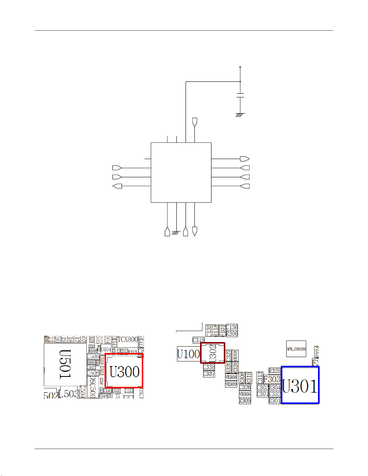
U300
I
K
Q
D
L
E
R
I
L
/
C
3
4
2
T
S
C
R
/
N
56
HPOUT-L/MONO
C
L
L
P
7
C337
C338
R324
SPK_CON200
R325
YAMA_OUT_R
YAMA_OUT_L
TCXO_OUT
R313
R312
C307
YMU_IRQ
YMU_RST_N
2-
C310
12
SAMSUNG Proprietary-Contents may change without notice
This Document can not be used without Samsung's authorization
YMU_2.8V
C311
SGH-Z320i Flow Chart of Troubleshooting and Circuit Diagrams
MSMP_2.6V
L
_
R
A
E
_
M
S
M
C318
AUD_SEL_1
YAMA_OUT_L
ICE_AMP_L
16
1
1S2
2
1-2IN
3
2S1
4
D2
5
15
1
D
U302
2
S
2
6
L
_
R
A
E
_
M
S
M
14
13
2
1
C
S
S
C
4
1
V
D
1
N
S
3
G
8
7
R
_
T
U
O
_
A
M
A
Y
3-4IN
3
D
R
_
R
A
E
D4
4S1
3S2
11
12
10
EAR_L
YAMA_OUT_L
AUD_SEL_2
9
MSM_EAR_R
- Layout for Speaker Part
SAMSUNG Proprietary-Contents may change without notice
This Document can not be used without Samsung's authorization
2-
13
SGH-Z320i Flow Chart of Troubleshooting and Circuit Diagrams
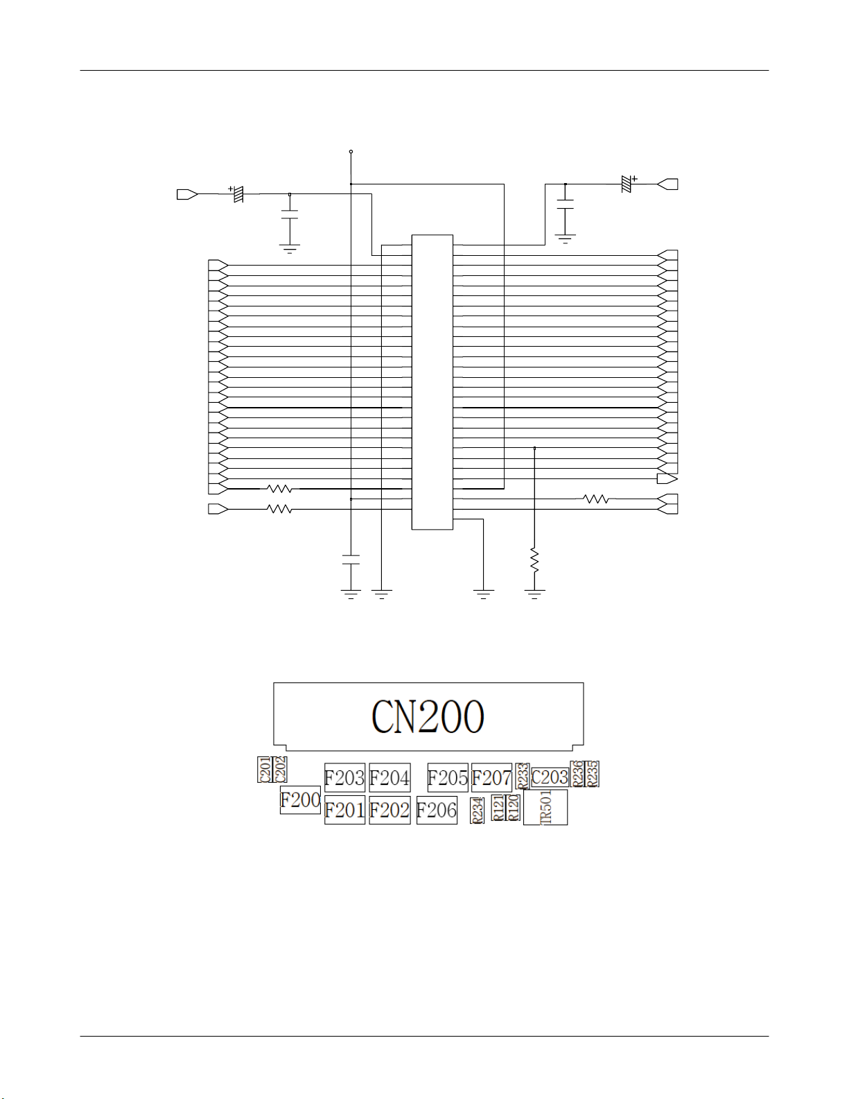
2-1-7. Receiver Part
There is no sound from receiver
Is the terminal of receiver
is ok ?
YES
Are there any signal
at the TA201,TA202
YES
Are there any signal
at the pin #2,3 of CN200?
YES
NO
NO
NO
Replace the receiver
Check the UCP100 & speaker
related circuit
Check the CN200 &
Resolder CN200
Is receiver working ?
NO
Replace the receiver
YES
END
14
2-
SAMSUNG Proprietary-Contents may change without notice
This Document can not be used without Samsung's authorization
SGH-Z320i Flow Chart of Troubleshooting and Circuit Diagrams
V_IN
VOICE_OUT_N
LCD_RESET_A
SVC_LED_ON
CAM_HSYNC
CAM_VSYNC
CAM_SCLA
CAM_SDAA
ENB_MEGA V_FLASH
TA201
C202
LCD_CS_A
LCD_D(1)
LCD_D(3)
LCD_D(5)
LCD_D(7)
LCD_D(9)
LCD_D(11)
LCD_D(13)
LCD_D(15)
KEY_1 KEY_2
KEY_3
SCAN_1 SCAN_4
CAM_D(0) CAM_D(1)
CAM_D(2)
CAM_D(4) CAM_D(5)
CAM_D(6)
MCLK
R233
R236
CN200
1
1
2
3
4
3
5
6
5
7
8
7
9
10
9
11
11 12
13
14
13
15
15 16
17
17 18
19
19
20
21
21 22
23
23 24
252526
27
27 28
29
29
30
31
31 32
33
33 34
35
36
35
37
37 38
39
39
40
41 42
41
42
43 44
43
44
45 46
45
46
47
48
47
49
50
49
51
51 52
53
53 54
55
2
4
6
8
10
12
14
16
18
20
22
24
26
28
30
32
34
36
38
40
48
50
52
54
55
C203
C201
R235
R234
TA202
VOICE_OUT_P
LCD_RS1_A
LCD_WE_A
LCD_D(0)
LCD_D(2)
LCD_D(4)
LCD_D(6)
LCD_D(8)
LCD_D(10)
LCD_D(12)
LCD_D(14)
KEY_0
SCAN_0
ON_SW
CAM_D(3)
CAM_D(7)
BL_EN
CAM_EN_B
CAM_RESET_N
PCLK
ENB_VGA
15
2-
SAMSUNG Proprietary-Contents may change without notice
This Document can not be used without Samsung's authorization
SGH-Z320i Flow Chart of Troubleshooting and Circuit Diagrams
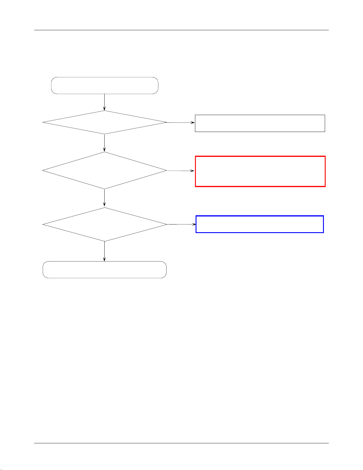
2-1-8. Headset Part
Headset function does not work
Check R508 is LOW ?
YES
Mic is not operational?
YES
Earphone is not operational?
YES
END
NO
NO
NO
Check the headset device, or R508 crack
1. Check the mic path from earjack
to MIC2P & MIC2N
2. Check the bias circuit
Check the ear path from earjack
to EAR_R & EAR_L
16
2-
SAMSUNG Proprietary-Contents may change without notice
This Document can not be used without Samsung's authorization
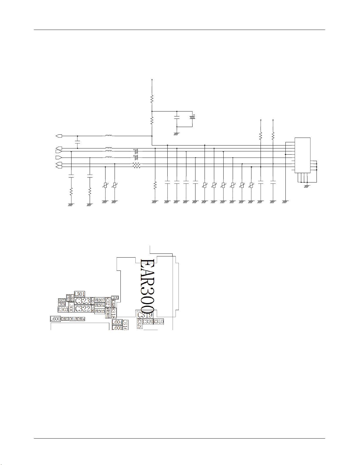
-SchmaticforEarmic
SGH-Z320i Flow Chart of Troubleshooting and Circuit Diagrams
MIC_2.85V
R329
MIC2P
MIC2N
EAR_R
C321
EAR_L
JACK_IN
EAR_SW
C324
R322
C325
R323
- Layout for Earmic
L300
L301
VR308
L306
L307
VR309
C322
C323
R308
R326
R321
R318
C328
C320
C329
(0603) (0603)(0603) (0603)
C330
C331
C319
VR302
VR307
VR303
VR304
VR305
MSMP_2.6V
VR306
MSMP_2.6V
R320
C327
R319
C326
10
11
33
55
77
99
EAR300
22
44
66
88
10
11GG12 13
GG
15
G
16
G
17
G
18
G
14
17
2-
SAMSUNG Proprietary-Contents may change without notice
This Document can not be used without Samsung's authorization
 Loading...