

Samsung SGH-Z110V Service Manual
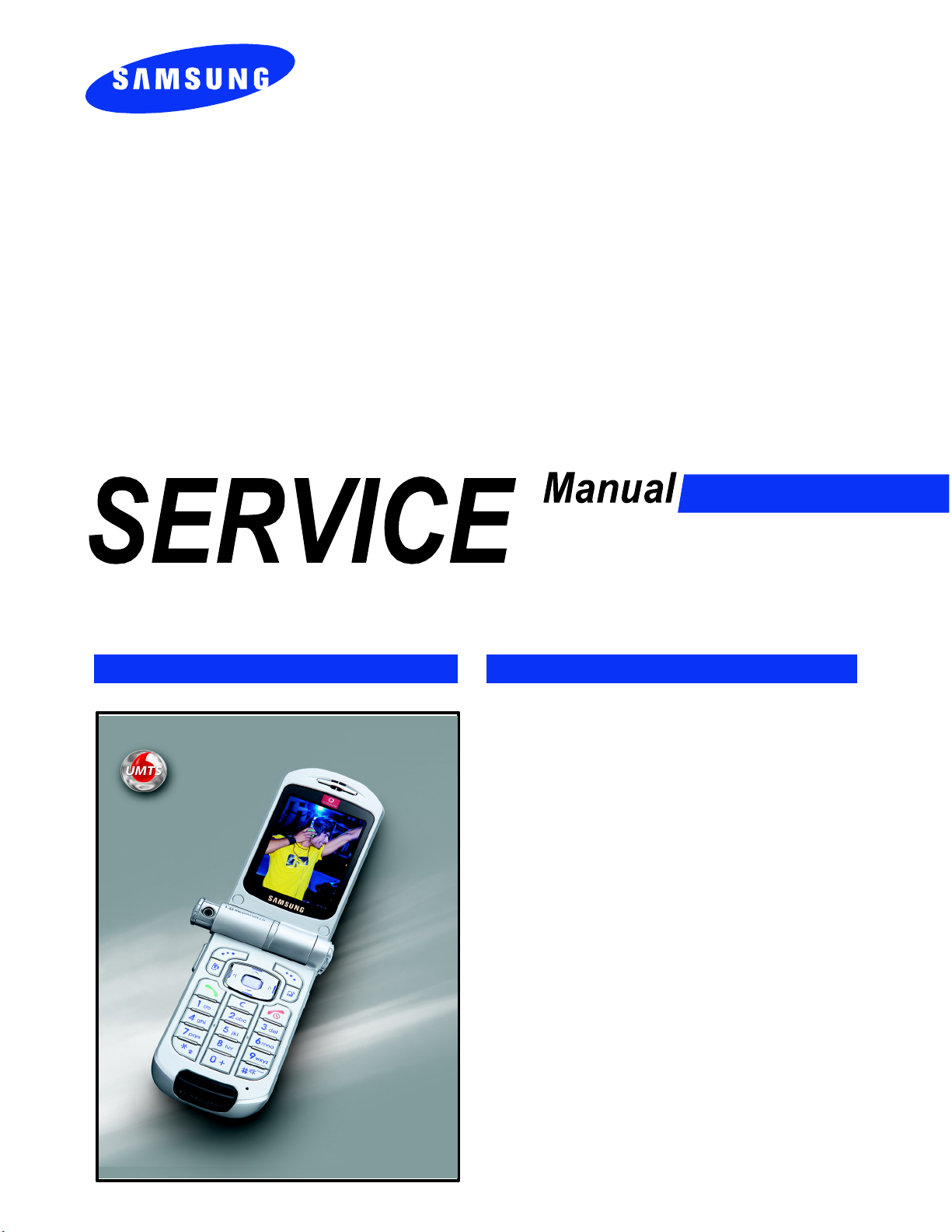
UMTS TELEPHONE
SGH-Z110V
UMTS TELEPHONE
CONTENTS
1. Specification
2. Circuit Description
3. Exploded Views and Parts List
4. Electrical Parts List
5. Block Diagrams
6. PCB Diagrams
7. Flow Chart of Troubleshooting
This Service Manual is a property of Samsung Electronics Co.,Ltd.
Any unauthorized use of Manual can be punished under applicable
International and/or domestic law.
ⓒ
Samsung Electronics Co.,Ltd. Nov. 2004
Samsung Electronics Co.,Ltd. Nov. 2004
Printed in South Korea.
Printed in South Korea.
Code No.:
BASIC.
GH68-05795A
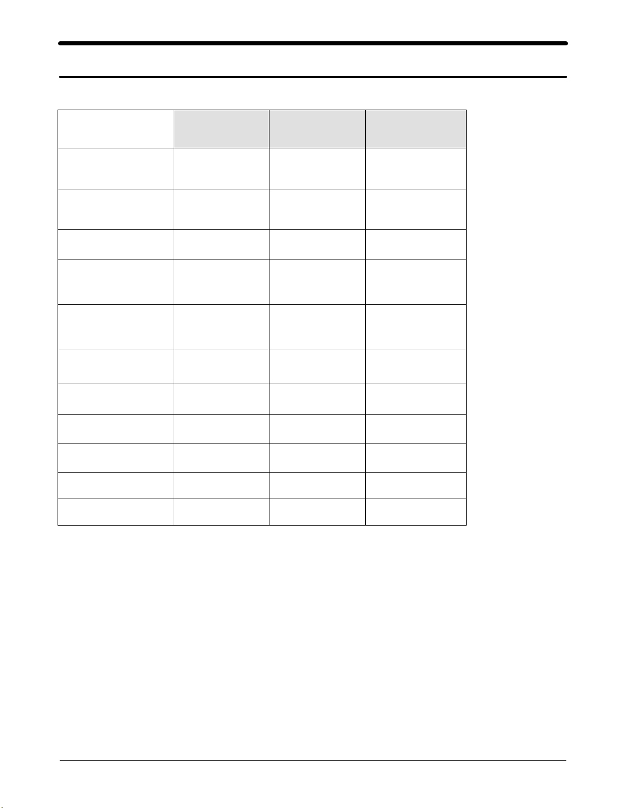
1. SGH-Z110V Specification
1. GSM General Specification
GSM900
Phase 1
Freq. Band[MHz]
Uplink/Downlink
ARFCN range 1~124
Tx/Rx spacing 45MHz 45MHz 95MHz
Mod. Bit rate/
Bit Period
Time Slot
Period/Frame
Period
Modulation 0.3GMSK 0.3GMSK 0.3GMSK
MS Power 33dBm~13dBm 33dBm~5dBm 30dBm~0dBm
890~915
935~960
270.833kbps
3.692us
576.9us
4.615ms
EGSM 900
Phase 2
880~915
925~960
0~124 &
975~1023
270.833kbps
3.692us
576.9us
4.615ms
DCS1800
Phase 1
1710~1785
1805~1880
512~885
270.833kbps
3.692us
576.9us
4.615ms
Power Class 5pcl ~ 15pcl 5pcl ~ 19pcl 0pcl ~ 15pcl
Sensitivity -102dBm -102dBm -100dBm
TDMA Mux 8 8 8
Cell Radius 35Km 35Km 2Km
1-1
SAMSUNG Proprietary-Contents may change without notice
This Document can not be used without Samsung's authorization
Specification
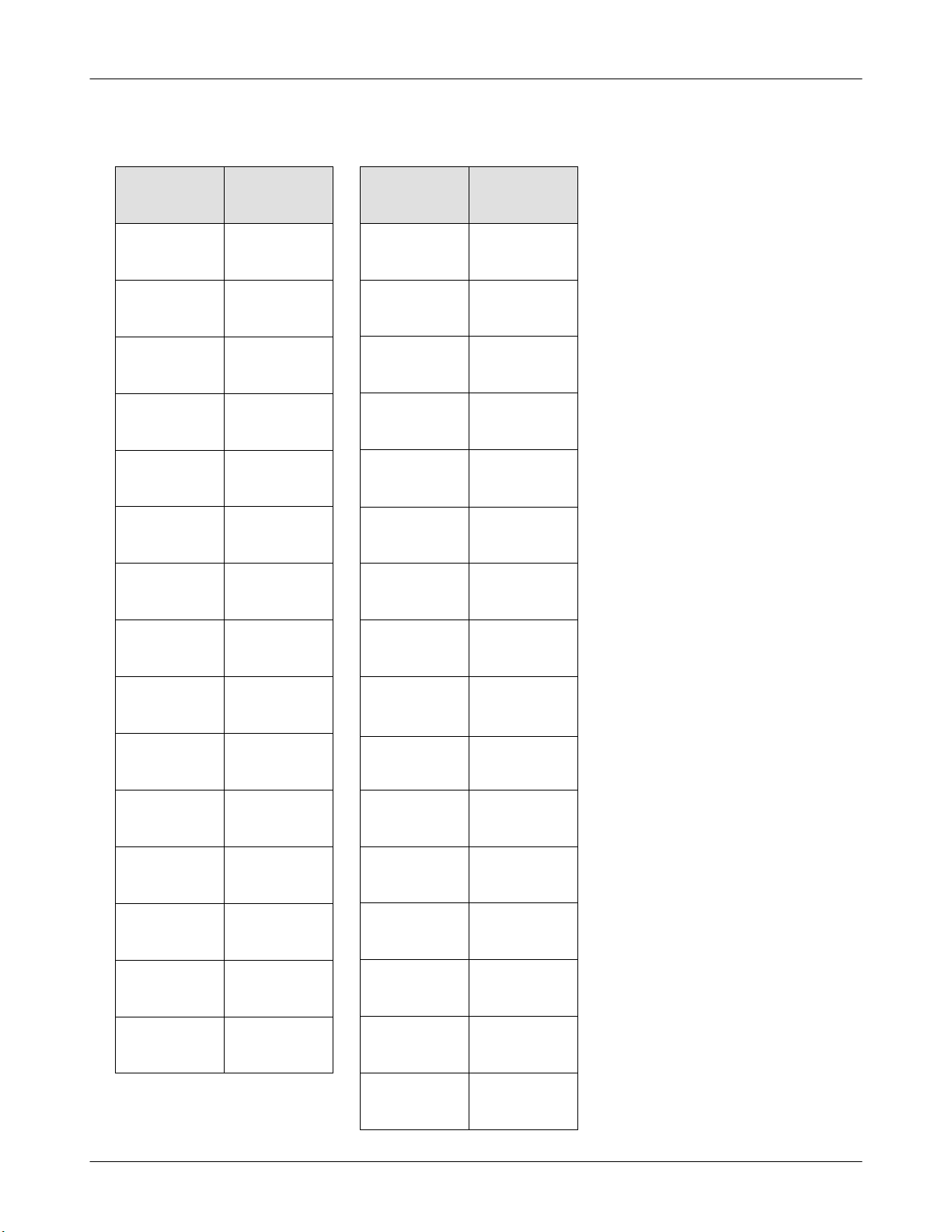
2. GSM TX power class
TX Pow er
control level
5 33±2 dBm
6 31±2 dBm
7 29±2 dBm
8 27±2 dBm
9 25±2 dBm
10 23±2 dBm
11 21±2 dBm
GSM900
TX Pow er
DCS1800
control level
0 30±3 dBm
1 28±3 dBm
2 26±3 dBm
3 24±3 dBm
4 22±3 dBm
5 20±3 dBm
6 18±3 dBm
12 19±2 dBm
13 17±2 dBm
14 15±2 dBm
15 13±2 dBm
16 11±3 dBm
17 9±3dBm
18 7±3 dBm
19 5±3 dBm
7 16±3 dBm
8 14±3 dBm
9 12±4 dBm
10 10±4 dBm
11 8±4dBm
12 6±4 dBm
13 4±4 dBm
14 2±5 dBm
15 0±5 dBm
1-2
SAMSUNG Proprietary-Contents may change without notice
This Document can not be used without Samsung's authorization

2. SGH-Z110V Circuit Description
1. SGH-Z110V RF Circuit Description
1. Antenna Switch Module (U100)
The antenna switch module allows multiple operating bands and modes to share the same antenna. A common
antenna connects to one of five paths: 1) UMTS-2100 Rx/Tx, 2) EGSM-900 Rx, 3) EGSM-900 Tx, 4) DCS-1800 Rx,
and 5) DCS-1800 Tx. UMTS operation requires simultaneous reception and transmission.
2. Filter
To convert Electromagnetic Field Wave to Acoustic Wave and then pass the specific frequency band.
- GSM Rx FILTER (F100)→For filtering the frequency band between 925 ~ 960 MHz.
- DCS Rx FILTER (F101)→For filtering the frequency band 1805 and 1880 MHz.
- WCDMA Rx FILTER (F200)→For filtering the frequency band 2110 and 2170 MHz.
- WCDMA Tx FILTER (F201)→For filtering the frequency band 1920 and 1980 MHz.
3. VCTCXO (OSC200)
To generate the 19.2MHz reference clock to drive the logic and RF.
4. Duplexer (F202)
A duplexer splits a single operating band into receive and transmit paths.
5. WCDMA PAM (U201)
This is a key component in the transmitter chain and must complement the RTR6200 IC precisely; jointly they
dominate the UMTS transmitter performance characteristics. Parameters such as gain, output power level, ACLR,
harmonics, Rx-band noise, and power supply current are critical.
6. GSM/DCS PAM (U102)
The PAM is a key component in any transmitter chain and must complement the rest of the transmitter precisely.
For GSM and DCS operation, the closed-loop transmit power control functions add even more requirements relative
to the UMTS PA. In addition to gain control and switching requirements, the usual RF parameters such as gain,
output power level, several output spectrum requirements, and power supply current are critical.
7. GSM/DCS Dual Tx VCO (OSC100)
The dual Tx VCO outputs, one for EGSM and one for DCS, drive a resistive network that splits the active signal
into two signals: 1) the input to the active PAM – this is the low loss path, and 2) the OPLL feedback signal.
8. Dual VCO (OSC201)
The dual-band UHF VCO is a key component within its phase-locked loop; VCO performance directly impacts PLL
and transceiver performance. GSM/DCS Rx/Tx LO & UMTS Rx LO signal is generated from this dual VCO's output.
9. RFL6200 (U200)
The RFL6200 includes an LNA circuit optimized for UMTS-2100 operation. The LNA is separated from all other
receive functions contained within the RFR6200 receiver IC to improve mixer LO to RF isolation – a critical
parameter in the Zero-IF architecture.
2-1
SAMSUNG Proprietary-Contents may change without notice
This Document can not be used without Samsung's authorization

Circuit Description
10. RFR6200 (U203)
The RFR6200 provides the Zero-IF receiver signal path, from RF to analog baseband, for UMTS-2100 applications.
The RFR6200 accepts its UMTS input signal from the handset RF front-end design. The UMTS input is configured
differentially to optimize second-order inter-modulation and common mode rejection performance, and implements
MSM-controlled gain adjustments to extend the receiver dynamic range.
11. RTR6200 (U101)
The RTR6200 supports multi-band, multi-mode phones with two receiver signal paths and three transmitter signal
paths:
1) Receiver paths
- EGSM-900
- DCS-1800
2) Transmitter paths
- EGSM-900 (using OPLL technique)
- DCS-1800 (using OPLL technique)
- UMTS-2100
Numerous secondary functions are integrated on-chip as well:
3) Phase-locked loop circuits
- PLL#1 and an on-chip VCO supports UMTS Tx
- PLL#2 and an external VCO supports EGSM Rx and Tx, DCS Rx and Tx, and UMTS Rx
4) Transceiver LO generation and distribution circuits
- EGSM-900 Rx and Tx
- DCS-1800 Rx and Tx
- UMTS-2100 Tx
2-2
SAMSUNG Proprietary-Contents may change without notice
This Document can not be used without Samsung's authorization

Circuit Description
2. Baseband Circuit description of SGH-Z110V
1. PM6050
1.1. Power Management
Ten low-dropout regulators designed specifically for GSM applications power the terminal and help ensure optimal
system performance and long battery life. It provides seven LDO support for 2.6V, 2.8V while a self-resetting,
electronically fused switch supplies power to external accessories. Ancillary support functions, such as RTC module
and RTC charger, Clock Buffer, aid in reducing both board area and system complexity.
SBI BUS serial interface provides access to control and configuration registers. This interface gives full control of
the MSM6200 and enables system designers to maximize both standby and talk times.
Supervisory functions. including a reset generator, an input voltage monitor, and a ADC support reliable system
design. These functions work together to ensure proper system behavior during start-up or in the event of a fault
condition(low microprocessor voltage, insufficient battery energy, or excessive die temperature).
1.2 TCXO Controller and Buffers
The PM6050 IC includes circuits for controlling the TCXO warm-up and buffering its signal for distribution throughout
the handset. Performance specifications are presented below.
2. Connector
2-1. LCD Connector
LCD is consisted of main LCD(color 262K TFT LCD) and small LCD(color 65K TFT LCD). Chip select signals in the
MA55141(U501), SLCD_CS can enable small LCD and DEN for main LCD. I2C buses in MSM6200 (U301) control
white-LED of LCDs.
"SLCD_RESET, MLCD_RESET" signals initiate the Reset process of LCDs.
8-bit data lines(RGB[10:17]) transfers data and commands to Small LCD through bypass capacitor. Data and
commands use "SCLD_RS" signal. If this signal is high, Inputs to Small LCD are commands. If it is low, Inputs to
Small LCD are data. The signal which informs the input or output state to Small LCD, is required.
Main LCD interface is 18bit data lines(RGB[0:17]) CPU Interface.
"RGB_VSYNC","RGB_HSYNC","RGB_DE",and,"RGB_CLK" are the signal for transferring data.
Power signals for LCD are "2.8VDV" and "VBATT". "SPKR_P","SPKL_P", "SPKR_N" and "SPKL_N" from U602 are
used for dual audio speaker.
2-2. Key
This is consisted of key interface pins among U301, KEY_0~3 and SCAN_0~6. These signals compose the matrix.
Result of the matrix informs the key status to key interface in U301. Power on/off key is seperated from the matrix.
So power on/off signal is connected with U301 to enable U400. Eighteen key LED use the "VCC_BK" supply voltage
from U304. "HALL_SW" informs the status of folder (open or closed) to modem. This uses the hall effect IC,EM1681.
A magnet under main LCD enables EM1681. It has additional two hall-effect ICs, that are needed for camera
sensing.
One senses the rotation of Z110V camera, and the other senses the Push-pull of the camera.
2-3
SAMSUNG Proprietary-Contents may change without notice
This Document can not be used without Samsung's authorization

Circuit Description
2-3. EMI ESD Filter
This system uses the EMI ESD filter, GMF05LC to protect ESD and Noise from IF CONNECTOR part, LCD,
Camra, and KEY PCB.
2-4. IF connetor
It is 24-pin connector. They are designed to use VBATT, VF, Q_TXD0, Q_RXD0, JIG_ON, M_RXD0, M_TXD0, USB
signal(D+,D-,USB_VCC) and GND. They connected to power supply IC, microprocessor and signal processor IC.
3. Audio
RCV_P and RCV_N from U601 are connected to the main receiver. EAR10P and EAR10N are connected to the
Earphone receiver. MIC1P and MIC1N are connected to the main MIC. And MIC2P and MIC2N are connected to
the Earphone.
YMU769 has a virtual speaker image function, so that it is the most suitable LSI as a sound source output device
which is used in mobile phones for high functional game sounds or high quality ringing melodies, and so on.
Synthesizer section in YMU769 adopts the “Stereophonic Hybrid Synthesizer System” that is given the advantages
of both FM Synthesizers and Wave Table Synthesizers, makes it possible to generate up to 32 FM voices and 32
wave table voices simultaneously.
YMU769 is a LSI for portable telephone that is capable of playing high quality music by utilizing FM synthesizer and
ADPCM decoder that are included in this device.
As a synthesis, YMU769 is equipped 32 voices with different tones. Since the device is capable of simultaneously
generating up to synchronous with the play of the FM synthesizer, various sampled voices can be used as sound
effects. Since the play data of YMU769 is interpreted at anytime through data bus, the length of the data(playing
period) is not limited, so the device can flexibly support application such as incoming call melody music distribution
service.
The hardware sequence built in this device allows playing of the complex music without giving excessive load to the
CPU of the portable telephones. Moreover, the registers of the FM synthesizer can be operated directly for real time
sound generation, allowing, for example, utilization of various sound effects when using the game software installed
in the portable telephone.
YMU769 includes a speaker amplifier with high ripple removal rate whose maximum output is 550mW (SPVDD=3.6V).
For the headphone, it is provided with a stereophonic output terminal.
4. Memory
The signals in the MSM6200 enable two memories. They use only one volt supply voltage, VDD_LP from the
PM6050. This system uses SPANSION's memory, S99PL129JCOBAWUC. It is consisted of 128M bits flash NOR
memory and 32M bits SRAM memory. It has 16 bit data line, AD[0~15] which is connected to MSM6200. It has 22
bit address lines, A[1~22]. ROM_CS and RAM_CS signals is chip select.
In the multi-media processor, it has two type of memories. One is 1GMbit NAND Flash memory and the other is
512Mbit SDRAM memory. Multi-media processor doesn't have a NAND memory interface. But we make a software
algorithm use for NAND memory.
2-4
SAMSUNG Proprietary-Contents may change without notice
This Document can not be used without Samsung's authorization

Circuit Description
5. Multi-media processor MA55141
MA55141 is an LSI, which is designed on 3GPP 3G-324M Standard for a video telephone system.
Since protocol software is external, MA55141 can run with another protocol like H.323 by changing its software.
MA55141 has ARM9 CPU, so supports more various application.
Feature
- Based on 3GPP 3G-324M standard
- Video MPEG-4 (simple profile level1) or H263 (baseline)
- Audio AMR, G723.1, MP3 or AAC (program downloadable)
- Multiplexing H.223 (Level 0, 1, 2, processed by CPU with assistant hardware)
- Control H.245 (Processed all by CPU)
- Built-in 32bit RISC CPU(ARM926EJ) for control. (Max 133MHz, I-cache 16KB, D-cache 8KB, MMU and JAVA
accelerator (Jazelle) included.)
- Built-in 16bit DSP for audio CODEC
- Built-in SD/MMC/Memory Stick I/F
- Video input Rec601/656 YUV = 4:2:2, 8 bit I/F
- Video output Rec601 YUV = 4:2:2(8bit) / RGB 18bit
Built-in Picture-In-Picture Image Displaying Functions
Built-in On Screen Display(OSD) Functions with alpha blending
- Video CODEC
Encoding and decoding : QCIF 40fps, CIF 10fps
Encoding only : QCIF 68fps, CIF 17fps
Decoding only : QCIF 96fps, CIF 24fps
Deblocking filter is built-in.
Max output image size : 2032×2032
- Program on SDRAM is executable without ROM (optional).
- Power supply
VDDI1=1.425V to 1.65V (For internal circuit. Please power off during stand-by)
VDDI2=VDDI1 (For internal circuit. Please provide during stand-by)
VDDP0, VDDP1=1.425V to 1.65V (For internal PLL0 and PLL1)
VDDO, VDDOD=2.7V to 3.0V (For I/O)
- Max operating frequency CPU clock = 133MHz
DSP clock = 100MHz
SDRAM clock = 100MHz
Video clock = SDRAM clock/2
6. MIC2211 (U604/U605)
This LDO is the voltage source of Multimedia part. The MIC2211 is a dual-output LDO regulator.
The one of dual is capable of sourcing 150mA, while the another one can supply up to 300mA.
Ideal for battery operated applications, the MIC2211 offers 1% accuracy, extremely low dropout voltage (80mV @
100mA), and extremely low ground current (only 48mA total). Equipped with TTL logic compatible enable pins, the
MIC2211 can be put into a zero-off-mode current state, drawing no current when disabled. Separate enable pins
allow individual control of each output voltage.
2-5
SAMSUNG Proprietary-Contents may change without notice
This Document can not be used without Samsung's authorization

Circuit Description
7. Camera (HV7151SP)
The HV7151SP is a highly integrated single chip CMOS color image sensor implemented by proprietary
Hynix 0.35um COMS sensor process realizing high sensitivity and wide dynamic range.
Total pixel array size is 1170 x 880 pixels are active. So, It can supports the picture below 1Mega-pixel snap shot.
Each active pixel composed of 4 transistors has a micro-lens to enhance sensitivity, and converts photon energy to
analog pixel voltage. On-chip 10bit Analog to Digital Converter(ADC) ditgitizes analog pixel voltage, and on-chip
Correlated Double Sampling(CDS) scheme reduces Fixed Pattern Noise(FPN) dramatically. The integration of sensor
function and image processing functions make HV7151SP especially very suitable for mobile imaging systems such
as IMT-2000.
8. Irda
This system uses IRDA module, HSDL_3208, Agilent's. This has signals, Input data and output data.
These signals are connected to MSN6200.
2-6
SAMSUNG Proprietary-Contents may change without notice
This Document can not be used without Samsung's authorization
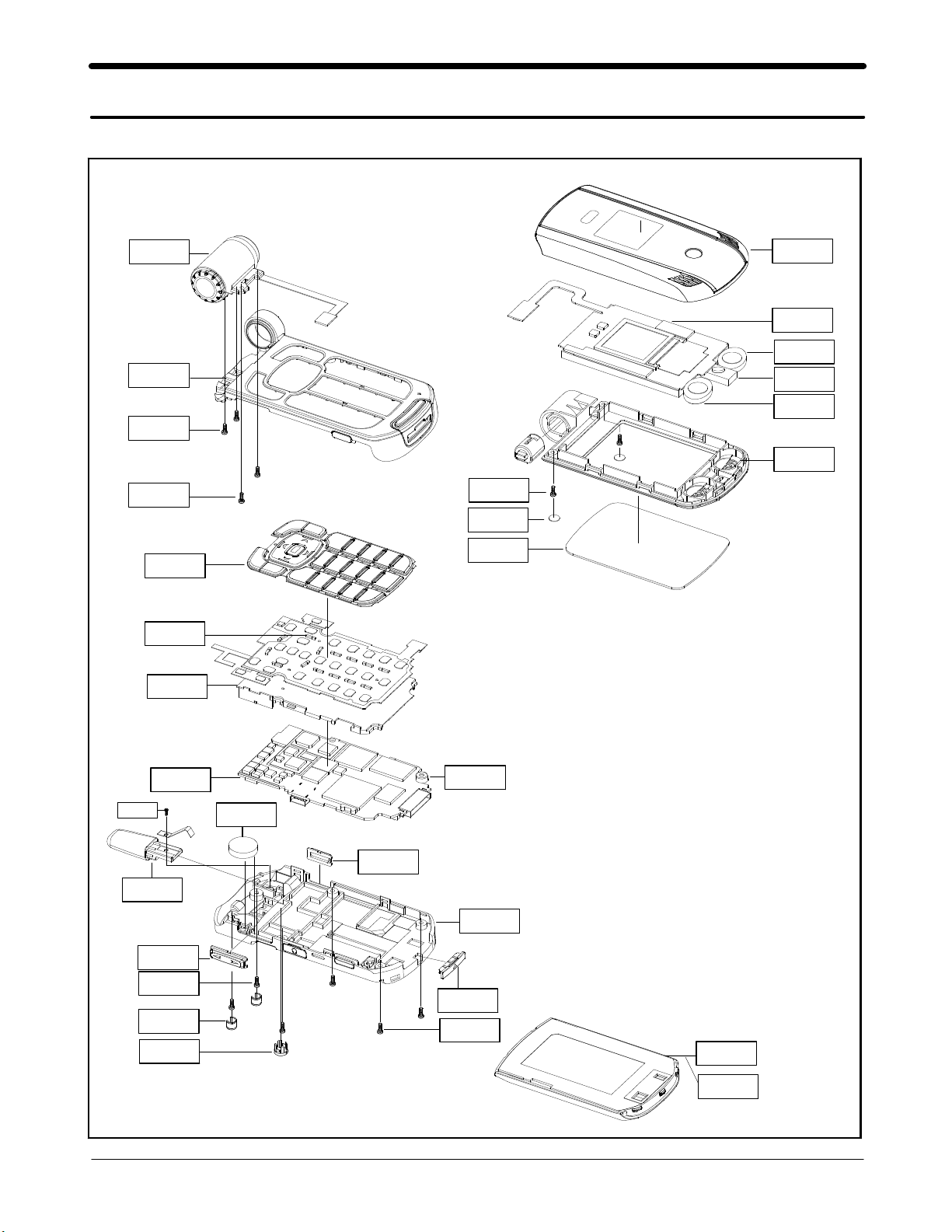
3. SGH-Z110V Exploded View and its Parts list
1. Cellular phone Exploded View
QCA01
QFR01
QCR42
QCR12
QKP01
QME01
QSH02
QFU01
QLC01
QSP02
QSP01
QSP03
QFL01
QCR20
QSC14
QMW01
QCR05
QAN01
QVO01
QCR26
QSC13
QRF01
QMP01
QMI01
QMO01
QVO02
QRE01
QIF01
QCR07
QBA32
QBA33
3-1
SAMSUNG Proprietary-Contents may change without notice
This Document can not be used without Samsung's authorization
Exploded view and its Part list
2. Cellular phone Parts list
Location
NO.
QFU01 FOLDER UPPER GH75-05245A
QLC01 LCD GH07-00614A
QSP01 SPEAKER 3001-001540
QSP02 SPEAKER 3001-001622
QSP03 SPEAKER 3001-001623
QFL01 FOLDER LOWER GH75-05246A
QCR20 SCREW 6001-001429
QSC14 FOLDER SCREW SHEET GH74-10909A
QMW01 MAIN WINDOW LCD GH72-16368A
QFR01 FRONT COVER GH75-05243A
QCA01 CAMERA GH59-01767A
QCR12 SCREW 6001-001530
QKP01 KEYPAD GH75-05247A
QME01 UNIT KEYPAD GH59-01768A
QSH02 SHIELD COVER GH71-04036A
QMP01 MAIN PBA GH92-01730A
QMI01 MICROPHONE ASSY GH30-00143A
QCR05 SCREW 6001-001478
QMO01 MOTOR 3101-001415
QVO02 KEY REJECT GH72-15405A
QVO01 KEY VOL GH72-15407A
QAN01 ANTENNA GH42-00488A
QRE01 REAR COVER GH75-05244A
QSC13 REAR SCREW CAP GH72-17726A
QRF01 RF COVER GH72-15400A
QIF01 IF COVER GH72-15401A
QCR07 SCREW 6001-001691
QCR26 SCREW 6001-001850
QCR42 SCREW 6001-001300
QBA32 BATTERY-860MAH GH43-01529A
QBA33 BATTERY-1360MAH GH43-01530A
Description SEC CODE Remark
3-2
SAMSUNG Proprietary-Contents may change without notice
This Document can not be used without Samsung's authorization
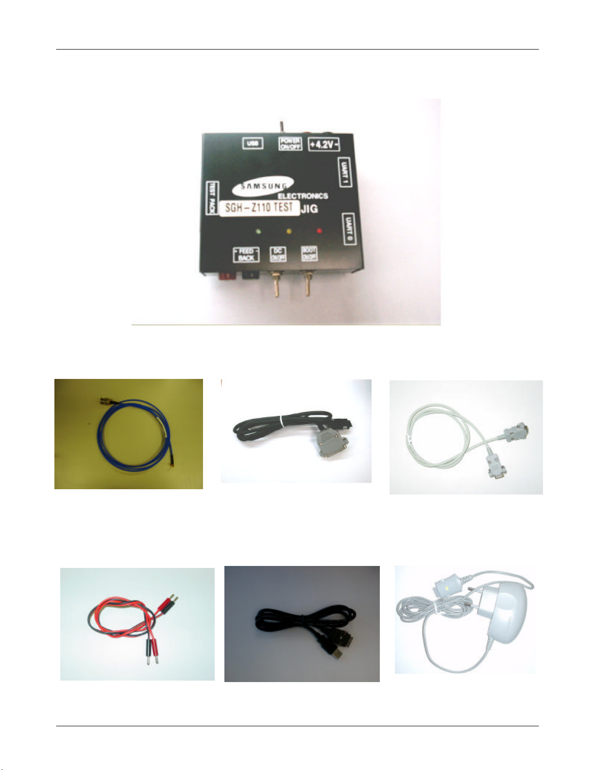
3. Test Jig (GH80-03308A)
Exploded view and its Part list
3-1. RF Test Cable
(GH39-00105A)
3-4. Power Supply Cable
3-2. Test Cable
(GH39-00337E)
3-5. DATA CABLE
(GH39-00326A)
3-3. Serial Cable
3-6. TC
(GH44-00701A)
3-3
SAMSUNG Proprietary-Contents may change without notice
This Document can not be used without Samsung's authorization
4. SGH-V110V MAIN Electrical Parts List
SEC Code Design LOC
0403-001387 ZD303
0403-001427 ZD304
0404-001153 ZD401
0404-001167 ZD308
0406-001178 ZD307
0406-001197 ZD300
0406-001197 ZD301
0406-001197 ZD302
0406-001197 ZD305
0406-001197 ZD400
0406-001197 ZD403
0406-001197 ZD404
0406-001197 ZD700
0406-001197 ZD701
0406-001197 ZD702
0406-001197 ZD703
0406-001197 ZD704
0406-001197 ZD705
0406-001197 ZD706
0406-001197 ZD707
0406-001197 ZD708
0406-001197 ZD709
0406-001197 ZD710
0406-001197 ZD711
0406-001197 ZD712
0406-001197 ZD713
0406-001197 ZD714
0406-001197 ZD715
0406-001197 ZD716
0406-001197 ZD717
0407-001002 ZD306
0407-001002 ZD402
0407-001038 U307
0504-001060 U202
0504-001113 Q201
0505-001423 U303
0505-001423 U305
0505-001423 U313
0505-001423 U608
SEC Code Design LOC
0505-001464 Q200
0505-001464 Q300
0604-001261 LED700
1001-001231 U205
1001-001231 U312
1001-001231 U402
1001-001288 U100
1001-001296 U306
1001-001296 U503
1001-001296 U601
1001-001306 U404
1109-001302 U300
1109-001317 U500
1201-001984 U200
1201-002174 U102
1201-002196 U201
1203-003007 U400
1203-003105 U302
1203-003105 U304
1203-003137 U403
1203-003275 U605
1203-003322 U604
1203-003359 U607
1203-003501 U401
1203-003563 U310
1203-003585 U700
1203-003591 U204
1204-002316 U602
1204-002354 U501
1205-002295 U301
1205-002297 U203
1205-002300 U101
1205-002530 U606
1205-002592 U308
1404-001224 TH300
1405-001082 V602
1405-001082 V603
2007-000138 R123
2007-000138 R202
4-1
SAMSUNG Proprietary-Contents may change without notice
This Document can not be used without Samsung's authorization
Electrical Parts List
SEC Code Design LOC
2007-000138 R209
2007-000140 R351
2007-000147 R125
2007-000148 R105
2007-000148 R111
2007-000148 R331
2007-000149 R352
2007-000160 R631
2007-000168 R321
2007-000171 R204
2007-000171 R205
2007-000171 R220
2007-000171 R628
2007-000171 R633
2007-000172 R112
2007-000173 R201
2007-000174 R733
2007-000242 R348
2007-000775 R408
2007-001119 R353
2007-001217 R113
2007-001217 R127
2007-001217 R128
2007-001284 R212
2007-001291 R114
2007-001291 R115
2007-001291 R224
2007-001291 R225
2007-001295 R116
2007-001298 R210
2007-001298 R211
2007-001301 R122
2007-001305 R121
2007-001307 R117
2007-001307 R118
2007-001307 R119
2007-001307 R120
2007-001313 R316
2007-001325 R109
SEC Code Design LOC
2007-001325 R607
2007-001339 R320
2007-001339 R322
2007-002796 R410
2007-002796 R514
2007-003006 R420
2007-003022 R731
2007-003022 R732
2007-007107 R219
2007-007107 R412
2007-007135 R334
2007-007137 R218
2007-007142 R126
2007-007314 R200
2007-007314 R206
2007-007314 R208
2007-007314 R333
2007-007318 R330
2007-007318 R615
2007-007318 R616
2007-007491 R110
2007-007491 R207
2007-007538 R327
2007-007698 R216
2007-007981 R421
2007-008045 R107
2007-008045 R124
2007-008045 R129
2007-008045 R306
2007-008045 R307
2007-008045 R308
2007-008045 R309
2007-008045 R700
2007-008045 R701
2007-008045 R702
2007-008045 R703
2007-008045 R704
2007-008045 R705
2007-008045 R706
4-2
SAMSUNG Proprietary-Contents may change without notice
This Document can not be used without Samsung's authorization
 Loading...