

Samsung S3C7515, S3P7515 Datasheet

PRODUCT OVERVIEW S3C7515/P7515
1 PRODUCT OVERVIEW
OVERVIEW
The S3C7515/P7515 single-chip CMOS microcontroller has been designed for high-performance using
Samsung's newest 4-bit CPU core, SAM47 (Samsung Arrangeable Microcontrollers). The S3P7515 is a
microcontroller which has 16-kbyte one-time-programmable EPROM but its functions are same to S3C7515.
With its DTMF generator, 8-bit serial I/O interface, and versatile 8-bit timer/counters, the S3C7515/P7515 offers
an excellent design solution for a wide variety of telecommunication applications.
Up to 55 pins of the 64-pin SDIP or QFP package can be dedicated to I/O. Seven vectored interrupts provide fast
response to internal and external events. In addition, the S3C7515/P7515's advanced CMOS technology
provides for low power consumption and a wide operating voltage range.
DEVELOPMENT SUPPORT0
The Samsung Microcontroller Development System, SMDS, provides you with a complete PC-based development environment for S3C7-series microcontrollers that is powerful, reliable, and portable. In addition to its
window-based program development structure, the SMDS tool set includes versatile debugging, trace, instruction
timing, and performance measurement applications. The Samsung Generalized Assembler (SAMA) has been
designed specifically for the SMDS environment and accepts assembly language sources in a variety of
microprocessor formats. SAMA generates industry-standard hex files that also contain program control data for
SMDS compatibility.
1–2
S MSUNG
S MSUN
G
ELECTRONICS
ELECTRONICS

S3C7515/P7515 PRODUCT OVERVIEW
FEATURES SUMMARY
Memory
— 512 × 4-bit RAM
— 16,384 × 8-bit ROM
55 I/O Pins
— Input only: 4 pins
— I/O: 43 pins
— N-channel open-drain I/O: 8 pins
Memory-Mapped I/O Structure
— Data memory bank 15
DTMF Generator
— 16 dual-tone frequencies for tone dialing
8-bit Basic Timer
— 4 interval timer functions
Two 8-bit Timer/Counters
— Programmable interval timer
— External event counter function
— Timer/counters clock outputs to TCLO0 and
TCLO1 pins
External clock signal divider
Serial I/O interface clock generator
Watch Timer
— Time interval generation: 0.5 s, 3.9 ms at 32.768
kHz
— 4 frequency outputs to the BUZ pin
8-bit Serial I/O Interface
— 8-bit transmit/receive mode
— 8-bit receive mode
— LSB-first or MSB-first transmission selectable
Bit Sequential Carrier
— Supports 8-bit serial data transfer in arbitrary
format
Interrupts
— 3 external interrupt vectors
— 4 internal interrupt vectors
— 2 quasi-interrupts
Power-Down Modes
— Idle: Only CPU clock stops
— Stop: System clock stops
Oscillation Sources
— Crystal, ceramic for main system clock
— Crystal oscillator for subsystem clock
— Main system clock frequency: 3.579545 MHz
(typical)
— Subsystem clock frequency: 32.768 kHz (typical)
— CPU clock divider circuit (by 4, 8, or 64)
Instruction Execution Times
— 0.67, 1.33, 10.7 µs at 6.0 MHz
— 1.12, 2.23, 17.88 µs at 3.579545 MHz
— 122 µs at 32.768 kHz
Operating Temperature
— – 40 °C to 85 °C
Operating Voltage Range
— 2.0 V to 5.5 V
Package Types
— 64 SDIP, 64 QFP
1-3

PRODUCT OVERVIEW S3C7515/P7515
FUNCTION OVERVIEW
SAM47 CPU
All S3C7-series microcontrollers have the advanced SAM47 CPU core. The SAM47 CPU can directly address up
to 32 K bytes of program memory. The arithmetic logic unit (ALU) performs 4-bit addition, subtraction, logical,
and shift-and-rotate operations in one instruction cycle and most 8-bit arithmetic and logical operations in two
cycles.
CPU REGISTERS
Program Counter
A 14-bit program counter (PC) stores addresses for instruction fetches during program execution. Usually, the PC
is incremented by the number of bytes of the fetched instruction. The one instruction fetch that does not
increment the PC is the 1-byte REF instruction which references instructions stored in a look-up table in the
ROM. Whenever a reset operation or an interrupt occurs, bits PC13 through PC0 are set to the vector address.
Stack Pointer
An 8-bit stack pointer (SP) stores addresses for stack operations. The stack area is located in general-purpose
data memory bank 0. The SP is 8-bit read/writeable and SP bit 0 must always be logic zero.
During an interrupt or a subroutine call, the PC value and the PSW are written to the stack area. When the
service routine has completed, the values referenced by the stack pointer are restored. Then, the next instruction
is executed.
The stack pointer can access the stack despite data memory access enable flag status. Since the reset value of
the stack pointer is not defined in firmware, you use program code to initialize the stack pointer to 00H. This sets
the first register of the stack area to data memory location 0FFH.
PROGRAM MEMORY
In its standard configuration, the 16,384 × 8-bit ROM is divided into four areas:
— 16-byte area for vector addresses
— 16-byte general-purpose area (0010–001FH)
— 96-byte instruction reference area
— 16,256-byte area for general-purpose program memory
The vector address area is used mostly during reset operations and interrupts. These 16 bytes can alternately be
used as general-purpose ROM.
The REF instruction references 2 x 1-byte or 2-byte instructions stored in reference area locations 0020H–
007FH. REF can also reference three-byte instructions such as JP or CALL. So that a REF instruction can
reference these instructions, however, the JP or CALL must be shortened to a 2-byte format. To do this, JP or
CALL is written to the reference area with the format TJP or TCALL instead of the normal instruction name.
Unused locations in the REF instruction look-up area can be allocated to general-purpose use.
1-4

S3C7515/P7515 PRODUCT OVERVIEW
DATA MEMORY
Overview
The 512 × 4 bit data memory has four areas:
— 32 × 4-bit working register area
— 224 × 4-bit general-purpose area in bank 0 which is also used as the stack area
— 256 × 4-bit general-purpose area in bank 1
— 128 × 4-bit area in bank 15 for memory-mapped I/O addresses
The data memory area is also organized as three memory banks — bank 0, bank 1, and bank 15. You use the
select memory bank instruction (SMB) to select one of the banks as working data memory.
Data stored in RAM locations are 1-, 4-, and 8-bit addressable. After a hardware reset, data memory initialization
values must be defined by program code.
Data Memory Addressing Modes
The enable memory bank (EMB) flag controls the addressing mode for data memory banks 0, 1, or 15. When the
EMB flag is logic zero, only locations 00H–7FH of bank 0 and bank 15 can be accessed. When the EMB flag is
set to logic one, all three data memory banks can be accessed based on the current SMB value.
Working Registers
The RAM's working register area in data memory bank 0 is also divided into four register banks. Each register
bank has eight 4-bit registers. Paired 4-bit registers are 8-bit addressable.
Register A can be used as a 4-bit accumulator and double register EA as an 8-bit extended accumulator; double
registers WX, WL, and HL are used as address pointers for indirect addressing.
To limit the possibility of data corruption due to incorrect register addressing, it is advisable to use bank 0 for
main programs and banks 1, 2, and 3 for interrupt service routines.
Bit Sequential Carrier
The bit sequential carrier (BSC) mapped in data memory bank 15 is a 8-bit general register that you can
manipulate using 1-, 4-, and 8-bit RAM control instructions.
Using the BSC register, addresses and bit locations can be specified sequentially using 1-bit indirect addressing
instructions. In this way, a program can generate 8-bit data output by moving the bit location sequentially,
incrementing or decrementing the value of the L register. You can also use direct addressing to manipulate data
in the BSC.
1-5
PRODUCT OVERVIEW S3C7515/P7515
CONTROL REGISTERS
Program Status Word
The 8-bit program status word (PSW) controls ALU operations and instruction execution sequencing. It is also
used to restore a program's execution environment when an interrupt has been serviced. Program instructions
can always address the PSW regardless of the current value of data memory access enable flags.
Before an interrupt is processed, the PSW is pushed onto the stack in data memory bank 0. When the routine is
completed, PSW values are restored.
IS1 IS0 EMB ERB
C SC2 SC1 SC0
Interrupt status flags (IS1, IS0), the enable memory bank and enable register bank flags (EMB, ERB), and the
carry flag (C) are 1- and 4-bit read/write or 8-bit read-only addressable. Skip condition flags (SC0–SC2) can be
addressed using 8-bit read instructions only.
Select Bank (SB) Register
Two 4-bit locations called the SB register store address values used to access specific memory and register
banks: the select memory bank register, SMB, and the select register bank register, SRB.
'SMB n' instructions select a data memory bank (0, 1, or 15) and store the upper four bits of the 12-bit data
memory address in the SMB register. The 'SRB n' instruction is used to select register bank 0, 1, 2, or 3, and to
store the address data in the SRB.
The instructions 'PUSH SB' and 'POP SB' move SMB and SRB values to and from the stack for interrupts and
subroutines.
CLOCK CIRCUITS
Main system and subsystem oscillation circuits generate the internal clock signals for the CPU and peripheral
hardware. The main system clock can use a crystal, ceramic, or RC oscillation source, or an externally-generated
clock signal. The subsystem clock requires either a crystal oscillator or an external clock source.
Bit settings in the 4-bit power control and system clock mode registers select the oscillation source, the CPU
clock, and the clock used during power-down mode. The internal system clock signal (fxx) can be divided internally to produce three CPU clock frequencies — fxx/4, fxx/8, or fxx/64.
INTERRUPTS
Interrupt requests may be generated internally by on-chip processes (INTB, INTT0, INTT1, and INTS) or
externally by peripheral devices (INT0, INT1, and INT4). There are two quasi-interrupts: INT2 and INTW.
INT2/KS0–KS7 detects rising/falling edges of incoming signals and INTW detects time intervals of 0.5 seconds
or 3.91 milliseconds at the watch timer clock frequency of 32.768 kHz. The following components support
interrupt processing:
— Interrupt enable flags
— Interrupt request flags
— Interrupt priority registers
— Power-down termination circuit
1-6

S3C7515/P7515 PRODUCT OVERVIEW
POWER-DOWN
To reduce power consumption, there are two power-down modes: idle and stop. The IDLE instruction initiates idle
mode and the STOP instruction initiates stop mode.
In idle mode, only the CPU clock stops while peripherals and the oscillation source continue to operate normally.
Stop mode effects only the main system clock — a subsystem clock, if used, continues oscillating. In stop mode,
main system clock oscillation stops completely, halting all operations except for a few basic peripheral functions.
RESET or an interrupt (with the exceptions of INT0) can be used to terminate either idle or stop mode.
RESETRESET
When a RESET signal occurs during normal operation or during power-down mode, the CPU enters idle mode
when the reset operation is initiated. When the standard oscillation stabilization interval (36.6 ms at 3.579545
MHz) has elapsed, normal CPU operation resumes.
I/O PORTS
The S3C7515/P7515 has 14 I/O ports. Pin addresses for all I/O ports are mapped in bank 15 of the RAM. There
are 4 input pins, 43 configurable I/O pins, and 8 n-channel open-drain I/O pins, for a total of 55 I/O pins. The
contents of I/O port pin latches can be read, written, or tested at the corresponding address using bit
manipulation instructions.
TIMERS and TIMER/COUNTERS
The timer function has four main components: an 8-bit basic interval timer, two 8-bit timer/counters, and a watch
timer. The 8-bit basic timer generates interrupt requests at precise intervals, based on the selected CPU clock
frequency.
The programmable 8-bit timer/counters are used for external event counting, generation of arbitrary clock
frequencies for output, and dividing external clock signals. The 8-bit timer/counter 0 generates a clock signal
(SCK) for the serial I/O interface.
The watch timer has an 8-bit watch timer mode register, a clock selector, and a frequency divider circuit. Its
functions include real-time and watch-time measurement, and frequency outputs for buzzer sound.
SERIAL I/O INTERFACE
The serial I/O interface supports the transmission or reception of 8-bit serial data with an external device. The
serial interface has the following functional components:
— 8-bit mode register
— Clock selector circuit
— 8-bit buffer register
— 3-bit serial clock counter
The serial I/O circuit can be set either to transmit-and-receive or to receive-only mode. MSB-first or LSB-first
transmission is also selectable. The serial interface operates with an internal or an external clock source, or using
the clock signal generated by the 8-bit timer/counter 0. To modify transmission frequency, the appropriate bits in
the serial I/O mode register (SMOD) must be manipulated.
1-7

PRODUCT OVERVIEW S3C7515/P7515
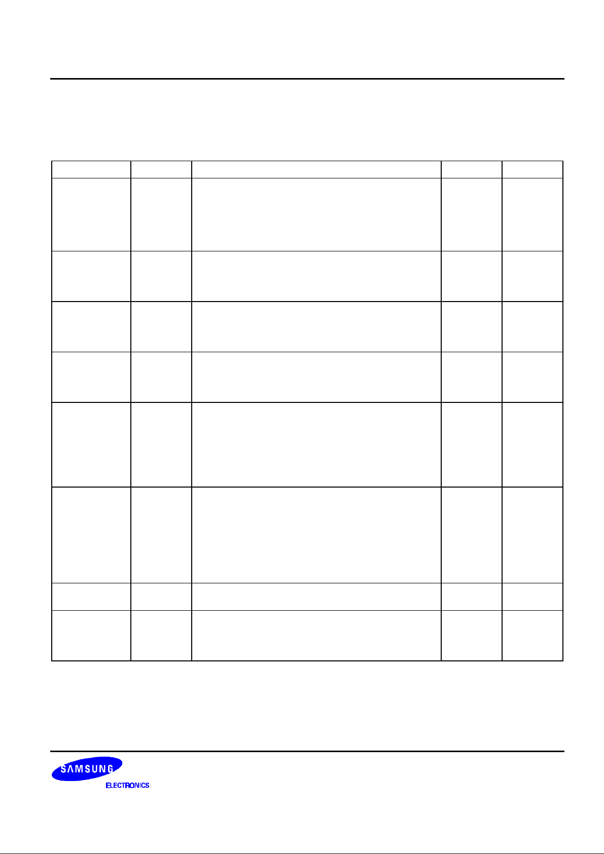
BLOCK DIAGRAM
P6.0–P6.3 /
KS0–KS3
P7.0–P7.3 /
KS4–KS7
P8.0–P8.3
P9.0–P9.3
P10.0–P10.3
P11.0–P11.3
P12.0–P12.3
P13.0–P13.2
INT0, INT1, INT2, INT4
8-BIT
TIMER/
COUNTER 0
8-BIT
TIMER/
COUNTER 1
I/O PORT 6
I/O PORT 7
I/O PORT 8
I/O PORT 9
I/O PORT 10
I/O PORT 11
I/O PORT 12
I/O PORT 13
Xin
RESET
INTERRUPT
CONTROL
XTin
CLOCK
BLOCK
INTERNAL
INTERRUPTS
INSTRUCTION DECODER
ARITHMETIC
AND
LOGIC UNIT
512 x 4-BIT
DATA
MEMORY
Xout
XTout
BASIC
TIMER
STACK
POINTER
PROGRAM
COUNTER
PROGRAM
STATUS WORD
FLAGS
16 K BYTE
PROGRAM
MEMORY
WATCH
TIMER
I/O PORT 0
SERIAL I/O
PORT
INPUT
PORT 1
I/O PORT 2
I/O PORT 3
I/O PORT 4
I/O PORT 5
DTMF
GENERATOR
P0.0 /
SCK
P0.1 / SO
P0.2 / SI
P0.3 / BTCO
P1.0 / INT0
P1.1 / INT1
P1.2 / INT2
P1.3 / INT4
P2.0 / TCLO0
P2.1 / TCLO1
P2.2 / CLO
P2.3 / BUZ
P3.0 / TCL0
P3.1 / TCL1
P3.2
P3.3
P4.0–P4.3
P5.0–P5.3
DTMF
1-8
Figure 1-1. S3C7515/P7515 Simplified Block Diagram

S3C7515/P7515 PRODUCT OVERVIEW
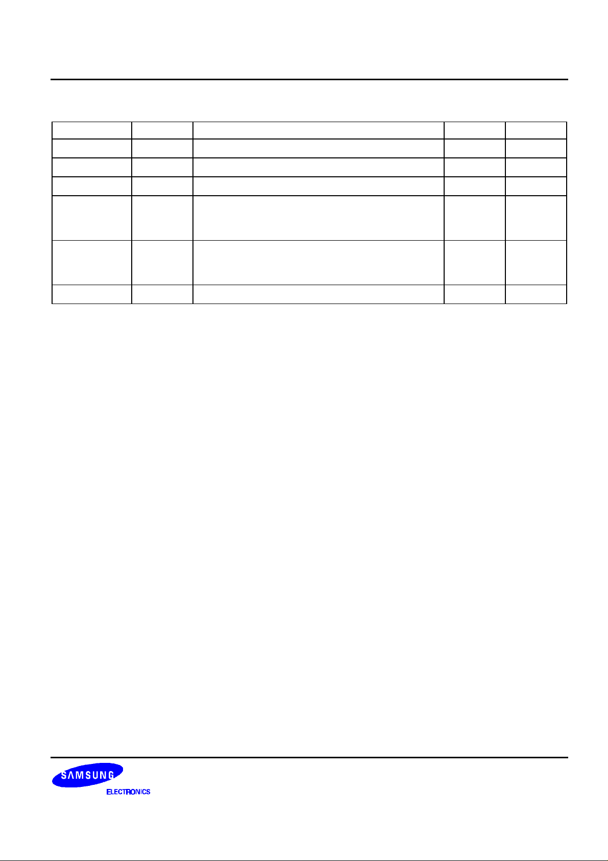
PIN ASSIGNMENTS
P1.3 / INT4
P1.2 / INT2
P1.1 / INT1
P1.0 / INT0
P13.2
P13.1
P13.0
P2.3 / BUZ
P2.2 / CLO
P2.1 / TCLO1
P2.0 / TCLO0
P0.3 / BTCO
P0.2 / SI
P0.1 / SO
P0.0 /
SCK
P10.3
P10.2
P10.1
P10.0
P11.3
P11.2
P11.1
P11.0
P12.3
P12.2
P12.1
P12.0
P3.3
P3.2
TEST
DTMF
VDD
1
2
3
4
5
6
7
8
9
10
11
12
13
14
15
16
17
18
19
20
21
22
23
24
25
26
27
28
29
30
31
32
(64-SDIP-750)
S3C7515
64
63
62
61
60
59
58
57
56
55
54
53
52
51
50
49
48
47
46
45
44
43
42
41
40
39
38
37
36
35
34
33
VSS
P9.0
P9.1
P9.2
P9.3
P8.0
P8.1
P8.2
P8.3
P7.0 / KS4
P7.1 / KS5
P7.2 / KS6
P7.3 / KS7
P6.0 / KS0
P6.1 / KS1
P6.2 / KS2
P6.3 / KS3
XTout
XTin
Xin
Xout
RESET
P5.0
P5.1
P5.2
P5.3
P4.0
P4.1
P4.2
P4.3
P3.0 / TCL0
P3.1 / TCL1
Figure 1-2. 64-SDIP Pin Assignment Diagrams
1-9

PRODUCT OVERVIEW S3C7515/P7515
P8.1
P8.2
P8.3
P7.0 / KS4
P7.1 / KS5
P7.2 / KS6
P7.3 / KS7
P6.0 / KS0
P6.1 / KS1
P6.2 / KS2
P6.3 / KS3
XTout
XTin
Xin
Xout
RESET
P5.0
P5.1
P5.2
51
50
49
48
47
46
45
44
43
42
41
40
39
38
37
36
35
34
33
32
31
30
29
28
27
26
25
24
23
22
21
20
P5.3
P4.0
P4.1
P4.2
P4.3
P3.0 / TCL0
P3.1 / TCL1
VDD
DTMF
TEST
P3.2
P3.3
P12.0
P8.0
P9.3
P9.2
P9.1
P9.0
VSS
P1.3 / INT4
P1.2 / INT2
P1.1 / INT1
P1.0 / INT0
P13.2
P13.1
P13.0
52
53
54
55
56
57
58
59
60
61
62
63
64
1 2 3 4 5 6 7 8 9
S3C7515
(64-QFP-1420F)
10
11
12
13
14
15
16
17
18
19
P10.3
P10.2
P10.1
P10.0
P11.3
P11.2
P11.1
P11.0
P12.3
P12.2
P12.1
P0.2 / SI
P0.1 / SO
P2.3 / BUZ
P2.2 / CLO
P2.1 / TCLO1
P2.0 / TCLO0
P0.0 / SCK
P0.3 / BTCO
Figure 1-2. 64-QFP Pin Assignment Diagrams (Continued)
1-10
S3C7515/P7515 PRODUCT OVERVIEW
PIN DESCRIPTIONS
Table 1-1. S3C7515/P7515 Pin Descriptions
Pin Name Pin Type Description Number Share Pin
P0.0
P0.1
P0.2
P0.3
P1.0
P1.1
P1.2
P1.3
P2.0
P2.1
P2.2
P2.3
P3.0
P3.1
P3.2
P3.3
P4.0–P4.3
P5.0–P5.3
P6.0–P6.3
P7.0–P7.3
P8.0–P8.3 I/O Same as port 0. 59–56
P9.0–P9.3 I/O 4-bit I/O port.
I/O 4-bit I/O port.
1-bit or 4-bit read/write and test is possible.
Individual pins are software configurable as input or
output.
4-bit pull-up resistors are software assignable; pull-up
resistors are automatically disabled for output pins.
I 4-bit input port.
1-bit and 4-bit read and test is possible.
4-bit pull-up resistors are assignable by software to
pins P1.0, P1.1, P1.2 and P1.3.
I/O Same as port 0. 11 (4)
I/O Same as port 0. 34 (27)
I/O 4-bit I/O ports.
N-channel open-drain output up to 9 volts.
1-bit and 4-bit read/write and test is possible.
Ports 4 and 5 can be paired to support 8-bit data
transfer.
8-bit unit pull-up resistors are assignable by mask
option.
I/O 4-bit I/O ports.
1-bit or 4-bit read/write and test is possible.
Port 6 pins are individually software configurable as
input or output.
4-bit pull-up resistors are software assignable; pull-up
resistors are automatically disabled for output pins
(port 6 only). Ports 6 and 7 can be paired to enable
8-bit data transfer.
1-bit or 4-bit read/write and test is possible.
4-bit pull-up resistors are software assignable; pull-up
resistors are automatically disabled for output pins.
15 (8)
14 (7)
13 (6)
12 (5)
1 (61)
2 (60)
3 (59)
4 (58)
10 (3)
9 (2)
8 (1)
33 (26)
29 (22)
28 (21)
38–35
(31–28)
42–39
(35–32)
51–48
(44–41)
55–52
(48–45)
(52–49)
63–60
(56–53)
SCK
SO
SI
BTCO
INT0
INT1
INT2
INT4
TCLO0
TCLO1
CLO
BUZ
TCL0
TCL1
–
KS0–KS3
KS4–KS7
–
–
* Parentheses indicate pin number for 64 QFP package.
1-11

PRODUCT OVERVIEW S3C7515/P7515
Table 1-1. S3C7515/P7515 Pin Descriptions (Continued)
Pin Name Pin Type Description Number Share Pin
P10.0–P10.3
P11.0–P11.3
P12.0–P12.3 I/O 4-bit I/O port.
P13.0–P13.2 I/O 3-bit I/O port; characteristics are same as port 9. 7–5
DTMF O DTMF output. 31 (24) –
SCK
SO I/O Serial data output 14 (7) P0.1
SI I/O Serial data input 13 (6) P0.2
BTCO I/O Basic timer clock output 12 (5) P0.3
INT0, INT1 I External interrupts. The triggering edge for INT0 and
INT2 I Quasi-interrupt with detection of rising edges 2 (59) P1.2
INT4 I External interrupt with detection of rising and falling
TCLO0 I/O Timer/counter 0 clock output 11 (4) P2.0
TCLO1 I/O Timer/counter 1 clock output 10 (3) P2.1
CLO I/O Clock output 9 (2) P2.2
BUZ I/O 2 kHz, 4 kHz, 8 kHz, or 16 kHz frequency output at
TCL0 I/O External clock input for timer/counter 0 34 (27) P3.0
TCL1 I/O External clock input for timer/counter 1 33 (26) P3.1
KS0–KS3
KS4–KS7
I/O Same as port 9.
Ports 10 and 11 can be paired to support 8-bit data
transfer.
1-bit or 4-bit read/write and test is possible.
Individual pins are software configurable as input or
output.
4-bit pull-down resistors are software assignable;
pull-down resistors are automatically disabled for
output pins.
I/O Serial I/O interface clock signal 15 (8) P0.0
INT1 is selectable. INT0 is synchronized to system
clock.
edges.
the watch timer clock frequency of 32.768 kHz for
buzzer sound
I/O Quasi-interrupt inputs with falling edge detection 51–48
19–16
(12–9)
23–20
(16–13)
27–24
(20–17)
(64–62)
4, 3
(61, 60)
1 (58) P1.3
8 (1) P2.3
(44–41)
55–52
(48–45)
P1.0, P1.1
P6.0–P6.3
P7.0–P7.3
–
–
–
* Parentheses indicate pin number for 64 QFP package.
1-12
S3C7515/P7515 PRODUCT OVERVIEW
Table 1-1. S3C7515/P7515 Pin Descriptions (Concluded)
Pin Name Pin Type Description Number Share Pin
V
DD
V
SS
RESET
XIN, X
XTIN, XT
OUT
OUT
– Power supply 32 (25) –
– Ground 64 (57) –
I Reset signal 43 (36) –
– Crystal, ceramic, or R/C oscillator signal for main
system clock. (For external clock input, use XIN and
input XIN's reverse phase to X
OUT
)
– Crystal oscillator signal for subsystem clock. (For
external clock input, use XTIN and input XTIN's
reverse phase to XT
OUT
)
45, 44
(38, 37)
46, 47
(39, 40)
–
–
NC – No connection (must be connected to VSS) 30 (23) –
* Parentheses indicate pin number for 64 QFP package.
1-13

PRODUCT OVERVIEW S3C7515/P7515
Table 1-2. Overview of S3C7515/P7515 Pin Data
Pin Names Share Pins I/O Type Reset Value Circuit Type
P0.0–P0.3
SCK, SO, SI, BTCO
P1.0–P1.3 INT0, INT1, INT2,
I/O Input D-4
I Input A-3
INT4
P2.0–P2.3 TCLO0, TCLO1, CLO,
I/O Input D-2
BUZ
P3.0–P3.1 TCL0, TCL1 I/O Input D-4
P3.2–P3.3 – I/O Input D-2
P4.0–P4.3
– I/O
(NOTE)
E-6
P5.0–P5.3
P6.0–P6.3
P7.0–P7.3
KS0–KS3
KS4–KS7
P8.0–P8.3 – I/O
P9.0–P9.3 – I/O
P10.0–P10.3
– I/O
I/O
Input
Input
Input
Input
D-4
D-2
D-2
D-2
P11.0–P11.3
P12.0–P12.3 – I/O
P13.0–P13.2 – I/O
DTMF – O
XIN, X
XTIN, XT
RESET
OUT
OUT
– – – –
–
I – B
Input
Input
High impedence
D-6
D-2
G-6
NC – – – –
VDD, V
SS
– – – –
NOTE: When pull-up resistors are provided: High level
When pull-up resistors are not provided: High impedence
1-14
 Loading...