

Samsung S3C72I9, S3P72I9 Datasheet

S3C72I9/P72I9 PRODUCT OVERVIEW
1 PRODUCT OVERVIEW
OVERVIEW
The S3C72I9 single-chip CMOS microcontroller has been designed for high performance using Samsung's
newest 4-bit CPU core, SAM47 (Samsung Arrangeable Microcontrollers).
With an up-to-896-dot LCD direct drive capability, 8-bit timer/counter 0, 16-bit timer/counter 1, and serial I/O, the
S3C72I9 offers an excellent design solution for a wide variety of applications which require LCD functions.
Up to 39 pins of the 100-pin QFP package can be dedicated to I/O. Eight vectored interrupts provide fast
response to internal and external events. In addition, the S3C72I9's advanced CMOS technology provides for low
power consumption and a wide operating voltage range.
OTP
The S3C72I9 microcontroller is also available in OTP (One Time Programmable) version, S3P72I9. S3P72I9
microcontroller has an on-chip 32 K-byte one-time-programable EPROM instead of masked ROM. The S3P72I9
is comparable to S3C72I9, both in function and in pin configuration.
1-1

PRODUCT OVERVIEW S3C72I9/P72I9
FEATURES SUMMARY
Memory
• 8,192 × 4-bit RAM (excluding LCD display RAM)
• 32,768 × 8-bit ROM
39 I/O Pins
• I/O: 35 pins
• Input only: 4 pins
LCD Controller/Driver
• 56 segments and 16 common terminals
• 8 and 16 common selectable
• Internal resistor circuit for LCD bias
• All dot can be switched on/off
8-bit Basic Timer
• 4 interval timer functions
• Watchdog timer
8-bit Timer/Counter 0
• Programmable 8-bit timer
Watch Timer
• Time interval generation: 0.5 s, 3.9 ms
at 32.768 Hz
• 4 frequency outputs to BUZ pin
• Clock source generation for LCD
Interrupts
• Four internal vectored interrupts
• Four external vectored interrupts
• Two quasi-interrupts
Bit Sequential Carrier
• Supports 16-bit serial data transfer in arbitrary
format
Power-Down Modes
• Idle mode (only CPU clock stops)
• Stop mode (main system clock and CPU clock
stop)
• Sub-system clock stop mode
• External event counter
• Arbitrary clock frequency output
• External clock signal divider
• Serial I/O interface clock generator
16-Bit Timer/Counter 1
• Programmable 16-bit timer
• External event counter
• Arbitrary clock frequency output
• External clock signal divider
8-bit Serial I/O Interface
• 8-bit transmit/receive mode
• 8-bit receive mode
• LSB-first or MSB-first transmission selectable
• Internal or external clock source
Memory-Mapped I/O Structure
• Data memory bank 15
Oscillation Sources
• Crystal, ceramic, or RC for main system clock
• Crystal oscillator for subsystem clock
• Main system clock frequency: 0.4 - 6 MHz
• Subsystem clock frequency: 32.768 kHz
• CPU clock divider circuit (by 4, 8, or 64)
Instruction Execution Times
• 0.67, 1.33, 10.7 µs at 6 MHz
• 0.95, 1.91, 15.3 µs at 4.19 MHz
• 122 µs at 32.768 kHz
Operating Temperature
• - 40 °C to 85 °C
Operating Voltage Range
• 1.8 V to 5.5 V (3.0 MHz @ 1.8 V)
Package Type
• 100-pin QFP
1-2

S3C72I9/P72I9 PRODUCT OVERVIEW
BLOCK DIAGRAM
P1.0-P1.3/
INT0-INT4
P2.0/CLO
P2.1/LCDCK
P2.2/LCDSY
P3.0/TCLO0
P3.1/TCLO1
P3.2/TCL0
P3.3/TCL1
P4.0-P4.3/
COM8-COM11
P5.0-P5.3/
COM12-COM15
P6.0-P6.3
SEG55-SEG52
KS4-KS7
P7.0-P7.3
SEG51-SEG48
P8.0-P8.3
SEG47-SEG44
P9.0-P9.3
SEG43-SEG40
Input Port 1
I/O Port 2
I/O Port 3
I/O Port 4
I/O Port 5
I/O Port 6
I/O Port 7
I/O Port 8
I/O Port 9
RESET
Interrupt
Control
Block
Internal
Interrupts
Instruction
Arithmetic
Logic Unit
8192 x 4-Bit
Memory
Data
and
XT
X
IN
IN
Clock
XT
X
OUT
OUT
Instruction
Register
Program
Status Word
Pointer
32 K Byte
Program
Memory
Basic
Timer
Stack
Watch
Timer
LCD
Driver/
Controller
Serial I/O
I/O
Port 0
8-Bit
Timer/
Counter 0
16-Bit
TImer/
Counter 1
VLC1-VLC5
COM0-COM7
P4.0-P5.3/
COM8-COM15
SEG0-SEG39
P9.3-P6.0/
SEG40-SEG55
P0.0/SCK/KO
P0.1/SO/K1
P0.2/SI/K2
P0.3/BUZ/K3
Figure 1-1. S3C72I9 Simplified Block Diagram
1-3

PRODUCT OVERVIEW S3C72I9/P72I9
PIN ASSIGNMENTS
SEG5
SEG6
SEG7
SEG8
SEG9
SEG10
SEG11
SEG12
SEG13
SEG14
SEG15
SEG16
SEG17
SEG18
SEG19
SEG20
SEG21
SEG22
SEG23
SEG24
99989796959493929190898887868584838281
SEG4
SEG3
SEG2
SEG1
SEG0
VLC5
VLC4
VLC3
VLC2
VLC1
P0.0/SCK/K0
P0.1/SO/K1
P0.2/SI/K2
P0.3/BUZ/K3
VDD
VSS
XOUT
XIN
TEST
XTIN
XTOUT
RESET
P1.0/INT0
P1.1/INT1
P1.2/INT2
P1.3/INT4
P2.0/CLO
P2.1/LCDCK
P2.2/LCDSY
P3.0/TCLO0
100
1
2
3
4
5
6
7
8
9
10
11
12
13
14
15
16
17
18
19
20
21
22
23
24
25
26
27
28
29
30
31323334353637383940414243444546474849
S3C72I9
(100-QFP-1420C)
80
79
78
77
76
75
74
73
72
71
70
69
68
67
66
65
64
63
62
61
60
59
58
57
56
55
54
53
52
51
50
SEG25
SEG26
SEG27
SEG28
SEG29
SEG30
SEG31
SEG32
SEG33
SEG34
SEG35
SEG36
SEG37
SEG38
SEG39
P9.3/SEG40
P9.2/SEG41
P9.1/SEG42
P9.0/SEG43
P8.3/SEG44
P8.2/SEG45
P8.1/SEG46
P8.0/SEG47
P7.3/SEG48
P7.2/SEG49
P7.1/SEG50
P7.0/SEG51
P6.3/SEG52/K7
P6.2/SEG53/K6
P6.1/SEG54/K5
1-4
COM0
COM1
COM2
COM3
COM4
COM5
COM6
COM7
P3.2/TCL0
P3.3/TCL1
P3.1/TCLO1
P4.0/COM8
P4.1/COM9
P4.2/COM10
P4.3/COM11
P5.0/COM12
P5.1/COM13
P5.2/COM14
P5.3/COM15
P6.0/SEG55/K4
Figure 1-2. S3C72I9 100-QFP Pin Assignment Diagram
S3C72I9/P72I9 PRODUCT OVERVIEW
PIN DESCRIPTIONS
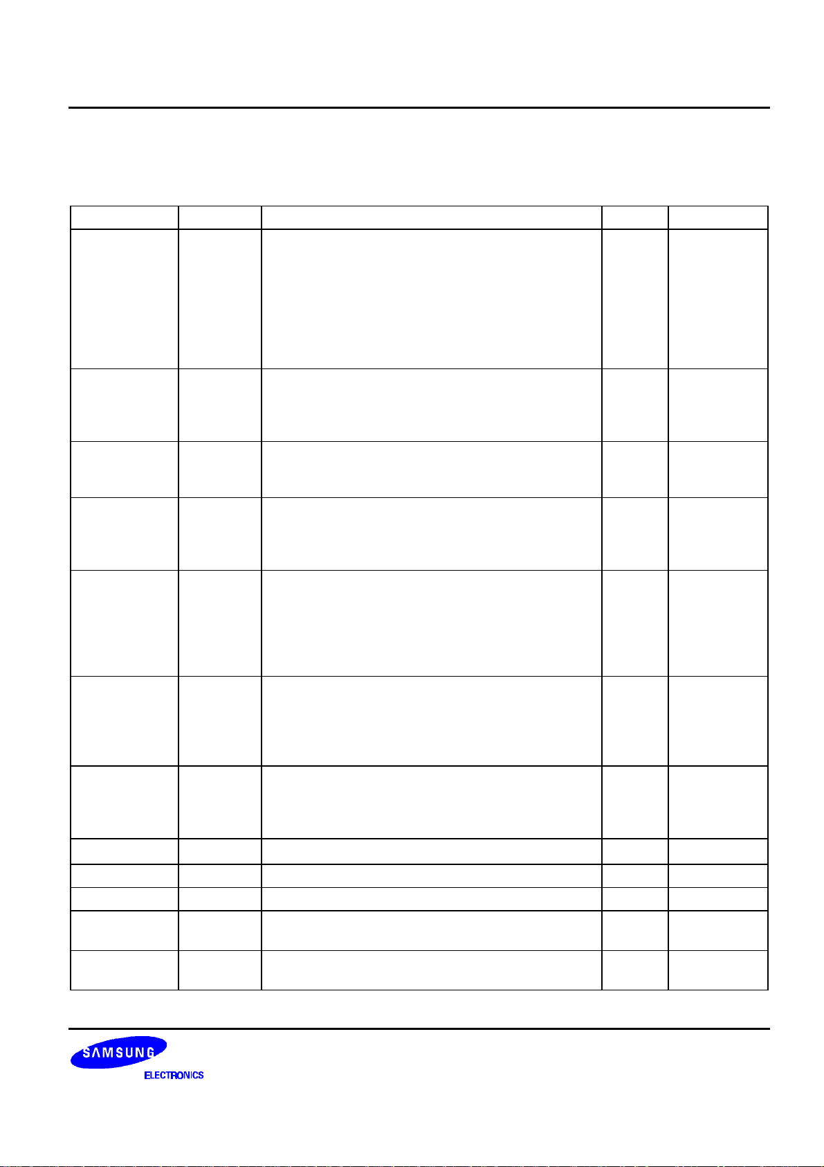
Table 1-1. S3C72I9 Pin Descriptions
Pin Name Pin Type Description Number Share Pin
P0.0
P0.1
P0.2
P0.3
P1.0
P1.1
P1.2
P1.3
P2.0
P2.1
P2.2
P3.0
P3.1
P3.2
P3.3
P4.0-P4.3
P5.0-P5.3
P6.0-P6.3
I/O 4-bit I/O port.
1-bit and 4-bit read/write and test are possible.
Individual pins are software configurable as input or
output.
11
12
13
14
Individual pins are software configurable as opendrain or push-pull output.
4-bit pull-up resistors are software assignable; pull-up
resistors are automatically disabled for output pins.
I 4-bit input port.
1-bit and 4-bit read and test are possible.
4-bit pull-up resistors are assignable by software.
23
24
25
26
I/O Same as port 0 except that port 2 is 3-bit I/O port. 27
28
29
I/O Same as port 0. 30
31
32
33
I/O 4-bit I/O ports.
42-45
1-, 4-bit or 8-bit read/write and test are possible.
Individual pins are software configurable as input or
46-49
output.
4-bit pull-up resistors are software assignable; pull-up
resistors are automatically disabled for output pins.
I/O Same as P4, P5. 50-53
SCK/K0
SO/K1
SI/K2
BUZ/K3
INT0
INT1
INT2
INT4
CLO
LCDCK
LCDSY
TCLO0
TCLO1
TCL0
TCL1
COM8-
COM11
COM12-
COM15
SEG55/K4-
SEG52/K7
P7.0-P7.3
54-57
SEG51-
SEG48
P8.0-P8.3
I/O Same as P4, P5. 58-61
SEG47-
SEG44
P9.0-P9.3
62-65
SEG43-
SEG40
SCK
I/O Serial I/O interface clock signal. 11 P0.0/K0
SO I/O Serial data output. 12 P0.1/K1
SI I/O Serial data input. 13 P0.2/K2
BUZ I/O 2 kHz, 4 kHz, 8 kHz or 16 kHz frequency output for
14 P0.3/K3
buzzer signal.
INT0, INT1 I External interrupts. The triggering edge for INT0 and
23, 24 P1.0, P1.1
INT1 is selectable.
1-5

PRODUCT OVERVIEW S3C72I9/P72I9
Table 1-1. S3C72I9 Pin Descriptions (Continued)
Pin Name Pin Type Description Number Share Pin
INT2 I Quasi-interrupt with detection of rising or
25 P1.2
falling edges.
INT4 I External interrupt with detection of rising or
26 P1.3
falling edges.
CLO I/O Clock output . 27 P2.0
LCDCK I/O LCD clock output for display expansion. 28 P2.1
LCDSY I/O LCD synchronization clock output for display
29 P2.2
expansion.
TCLO0 I/O Timer/counter 0 clock output. 30 P3.0
TCLO1 I/O Timer/counter 1 clock output. 31 P3.1
TCL0 I/O External clock input for timer/counter 0. 32 P3.2
TCL1 I/O External clock input for timer/counter 1. 33 P3.3
COM0-COM7 O LCD common signal output. 34-41 –
COM8-COM11 I/O 42-45 P4.0-P4.3
COM12-COM15 46-49 P5.0-P5.3
SEG0-SEG39 O LCD segment signal output. 5-1,
–
100-66
SEG40-SEG43 I/O 65-62 P9.3-P9.0
SEG44-SEG47 61-58 P8.3-P8.0
SEG48-SEG51 57-54 P7.3-P7.0
SEG52-SEG55 53-50 P6.3/K7-P6.0/K4
K0-K3 I/O External interrupt. The triggering edge is
11-14 P0.0-P0.3
selectable.
K4-K7 50-53 P6.0-P6.3
V
DD
V
SS
RESET
V
LC1-VLC5
X
in, Xout
– Main power supply. 15 –
– Ground. 16 –
I Reset signal. 22 –
– LCD power supply. 10-6 –
– Crystal, Ceramic or RC oscillator pins for
18, 17 –
system clock.
XT
in, XTout
TEST I
– Crystal oscillator pins for subsystem clock. 20, 21 –
Test signal input. (must be connected to VSS)
19 –
NOTE: Pull-up resistors for all I/O ports are automatically disabled if they are configured to output mode.
1-6
S3C72I9/P72I9 PRODUCT OVERVIEW
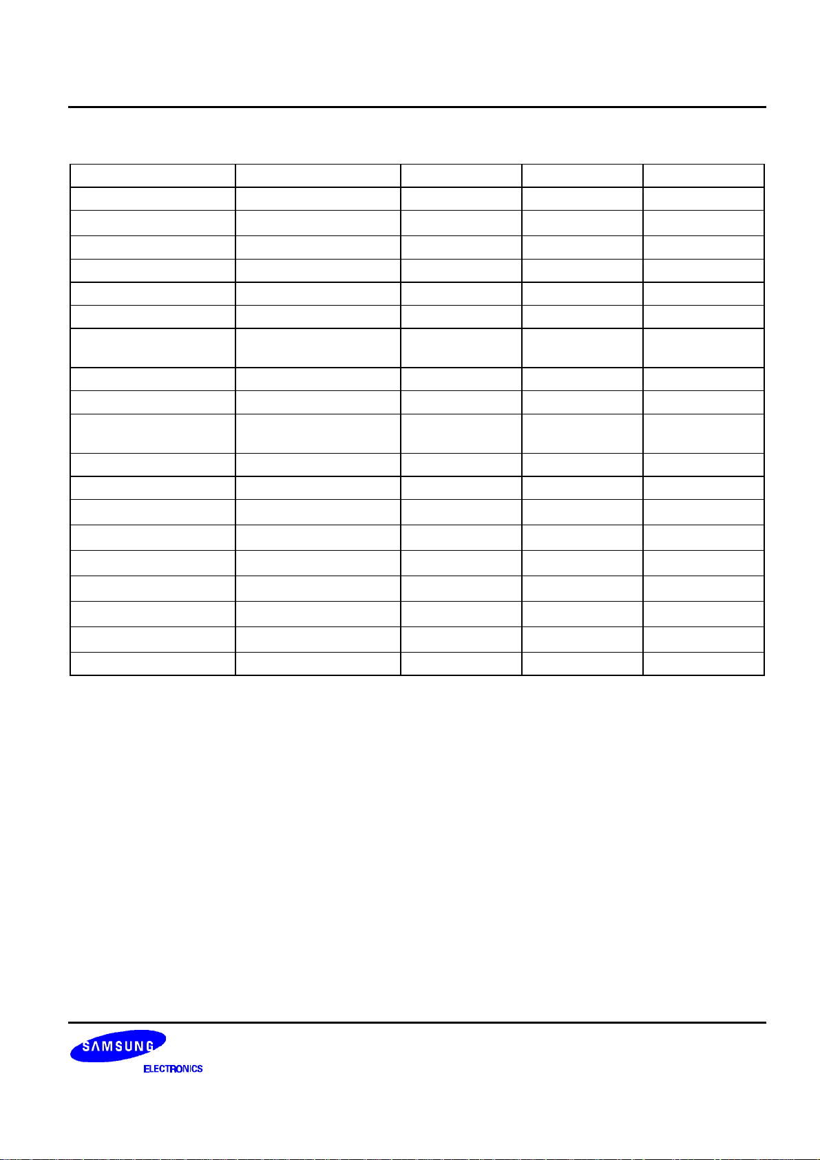
Table 1-2. Overview of S3C72I9 Pin Data
Pin Names Share Pins I/O Type Reset Value Circuit Type
P0.1, P0.3 SO/K1, BUZ/K3 I/O Input E-1
P0.0, P0.2
SCK/K0, SI/K2
I/O Input E-2
P1.0-P1.3 INT0-INT2, INT4 I Input A-3
P2.0-P2.2 CLO, LCDCK, LCDSY I/O Input E
P3.0-P3.1 TCLO0, TCLO1 I/O Input E
P3.2-P3.3 TCL0, TCL1 I/O Input E-1
P4.0-P4.3
P5.0-P5.3
P6.0-P6.3 SEG55/K4-SEG52/K7
COM8-COM11
COM12-COM15
I/O Input H-13
I/O
Input
H-16
P7.0-P7.3 SEG51-SEG48 I/O Input H-13
P8.0-P8.3
P9.0-P9.3
SEG47-SEG44
SEG43-SEG40
I/O
Input
H-13
COM0-COM7 – O High H-3
SEG0-SEG39 – O High H-15
V
DD
V
SS
RESET
V
V
-
LC1
X
X
IN,
XT
IN,
LC5
OUT
XT
OUT
– – – –
– – – –
– I – B
– – – –
– – – –
– – – –
TEST – I – –
1-7
PRODUCT OVERVIEW S3C72I9/P72I9
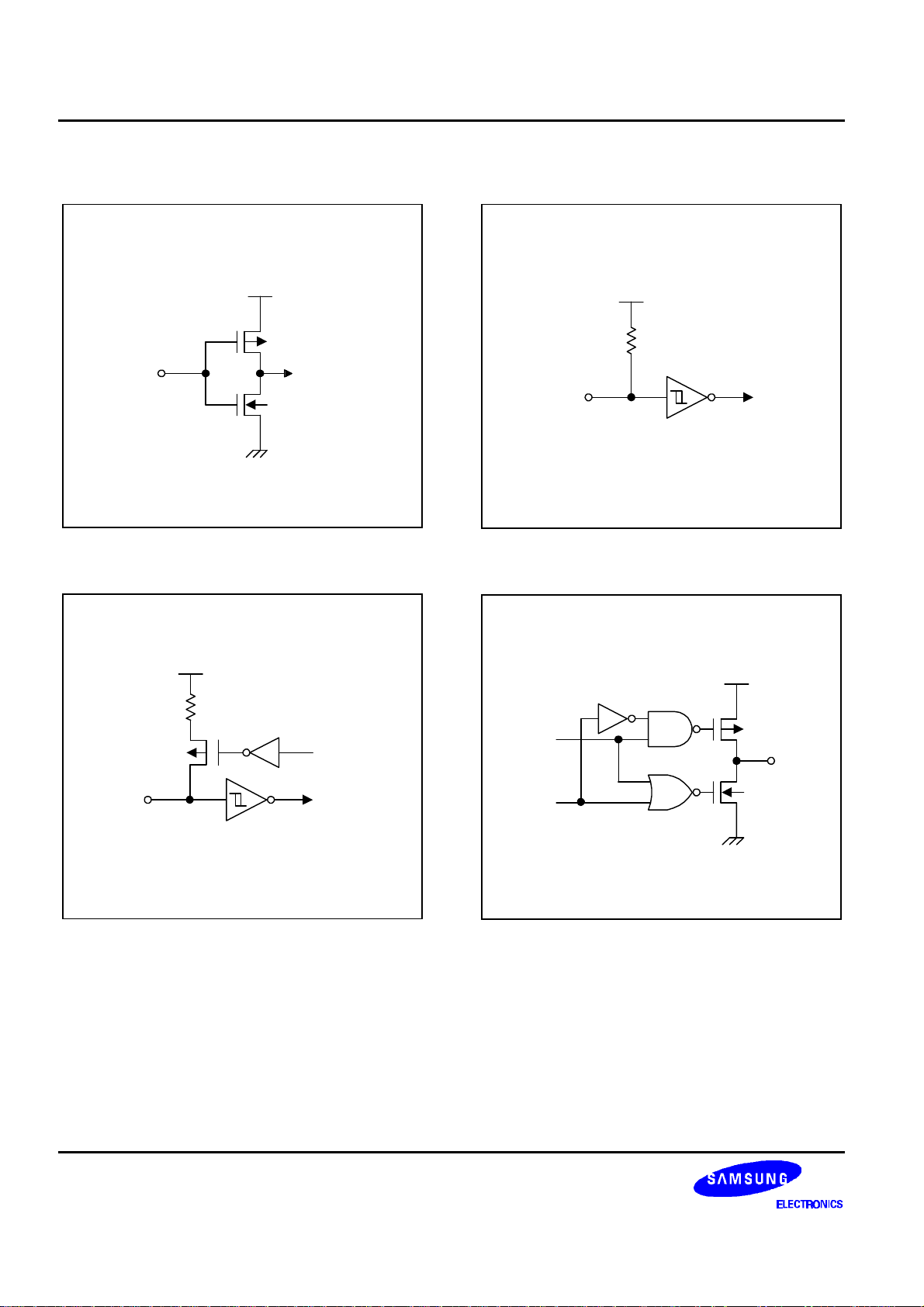
PIN CIRCUIT DIAGRAMS
VDD
P-Channel
In
N-Channel
Figure 1-3. Pin Circuit Type A
VDD
Pull-Up
Resistor
P-Channel
In
Pull-Up
Resistor
Enable
Data
Output
DIsable
VDD
Pull-Up
Resistor
In
Schmitt Trigger
Figure 1-5. Pin Circuit Type B
VDD
P-Channel
Out
N-Channel
1-8
Schmitt Trigger
Figure 1-4. Pin Circuit Type A-3
Figure 1-6. Pin Circuit Type C

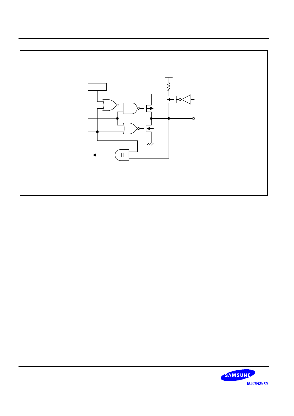
S3C72I9/P72I9 PRODUCT OVERVIEW
VDD
Data
Output
DIsable
PNE
Pull-up
VDD
P-CH
N-CH
Resistor
Figure 1-7. Pin Circuit Type E
VDD
Pull-up
Resistor
Enable
I/O
Data
Output
DIsable
PNE
Schmitt Trigger
VDD
Figure 1-8. Pin Circuit Type E-1
P-CH
N-CH
Pull-up
Resistor
Pull-up
Resistor
Enable
I/O
1-9
PRODUCT OVERVIEW S3C72I9/P72I9
VDD
Data
Output
DIsable
PNE
Schmitt Trigger
VDD
Figure 1-9. Pin Circuit Type E-2
P-CH
N-CH
Pull-up
Resistor
Pull-up
Resistor
Enable
I/O
1-10
 Loading...