

Samsung S3C72H8, S3P72H8 Datasheet
S3C72H8/P72H8 PRODUCT OVERVIEW
1 PRODUCT OVERVIEW
OVERVIEW
The S3C72H8 single-chip CMOS microcontroller has been designed for very high performance using Samsung's
state-of-the-art 4-bit product development approach, SAM47 (Samsung Arrangeable Microcontrollers). Its main
features are an up-to-13-digit LCD direct drive capability, 2-channel comparator inputs and outputs, and versatile
8-counter/ timers and 16-bit frequency counter. The S3C72H8 gives you an excellent design solution for a variety
of LCD-related applications, specially thermostat control application.
Up to 21 pins of the available 64-pin QFP packages can be dedicated to I/O. And six vectored interrupts provide
fast response to internal and external events.
In addition, the S3C72H8's advanced CMOS technology provides for low power consumption and a wide operating voltage range.
1-1

PRODUCT OVERVIEW S3C72H8/P72H8
FEATURES
Architecture
– SAM47 4-bit CPU core
Memory
– Data Memory: 512 × 4 bits
– Program Memory: 8196 × 8 bits
(Including LCD display RAM)
Memory-Mapped I/O Structure
– Data memory bank 15
Interrupts
– Three internal vectored interrupts
– Three external vectored interrupts
– Two quasi-interrupts
8-Bit Timer/Counter (T0)
– Programmable 8-bit timer
– External event counter
– Arbitrary clock frequency output
– External clock signal divider
16-Bit Frequency Counter (FC)
– a 16-bit binary up-counter
– External event counter
– Gate function control
Watch-Dog TIMER and Basic Timer
LCD Controller/Driver
– 26 segment and 4 common terminals
– Maximum 13-digit LCD direct drive capability
– Display modes: Static, 1/2, 1/3, 1/4 duty
– Voltage regulator and booster (1/3 bias: 1, 2, or
3V, 1/2 bias: 1.5, 3V)
Analog Comparator
– 2 Ch Comparator (Each CnP, CnN, CnOUT pins)
Bit Sequential Carrier
– Support 16-bit serial data transfer in arbitrary
format
I/O Ports
– 21 pins for standard I/O
– 26 pins for LCD segment output
– 4 pins for LCD common output
– Two input pins for external interrupts
Oscillation Sources
– Crystal, ceramic, or RC for main system clock
– Crystal or external oscillator for subsystem clock
– Main system clock frequency: 4.19 MHz (typical)
– Subsystem clock frequency: 32.768 kHz
– CPU clock divider circuit (by 4, 8, or 64 main, and
by 4 for sub clock)
– 8-bit counter + 3-bit counter
– Overflow signal of 8-bit counter makes a basic
timer interrupt. And control the oscillation warmup time
– Overflow signal of 3-bit counter makes a system
reset
Watch Timer
– Real-time and interval time measurement
– Four frequency outputs to buzzer sound
– Clock source generation for LCD
1-2
Power Down Mode
– Idle mode (only CPU clock stops)
– Stop mode (main or sub-system oscillation stops)
Voltage Level Detector
– VDD level detection circuit (2.2, 2.4, 3, or 4.0V)
– External pin level detect mode
Operating Voltage Range
– 1.8V to 5.5V at 3 MHz
– 2.0V to 5.5V at 4.19 MHz
Package Type
– 64-pin QFP

S3C72H8/P72H8 PRODUCT OVERVIEW
BLOCK DIAGRAM
SCLK
VPP/
XT
Clock
XTIN
OUT
TEST
Block
SDAT
OTP
Voltage
Level
Detector
Instruction
Register
Program
Counter
Program
Status
Word
Stack
Pointer
Two Analog
Comparator
Watch
Timer
Basic
Timer
16-Bit FREQ
Counter
8-Bit
Timer
LCD Driver/
Controller
Voltage
Booster
Watchdog
Timer
FCL
C0OUT
C1OUT
TCL0
TCLO0
COM0-COM3
SEG0-SEG25
CA, CB
VLC0-VLC2
P0.0/ExtRef
P0.1/SDAT
P0.2/SCLK
P2.0/INT0
P2.1/INT1
P2.2/TCL0
P2.3/FCL
P3.0/TCLO0
P3.1/BTCO
P3.2/CLO
P3.3/BUZ
P4.0/C0P
P4.1/C0N
P4.2/C0OUT
P4.3/C1OUT
P5.0/C1P
P5.1/C1N
P6.0/KS0
P6.1/KS1
P6.2/KS2
P6.3/KS3
I/O Port 0
I/O Port 2
I/O Port 3
I/O Port 4,5
I/O Port 6
INT0, INT1
512 x 4-Bit
Data
Memory
RESET
X
Interrupt
Control
Block
Internal
Interrupts
Instruction Decoder
Arithmetic
Logic Unit
8 K Byte
Program
Memory
XIN
OUT
and
ExtRef CnP
Cn
CnN
OUT
Figure 1-1. S3C72H8 Simplified Block Diagram
1-3
PRODUCT OVERVIEW S3C72H8/P72H8
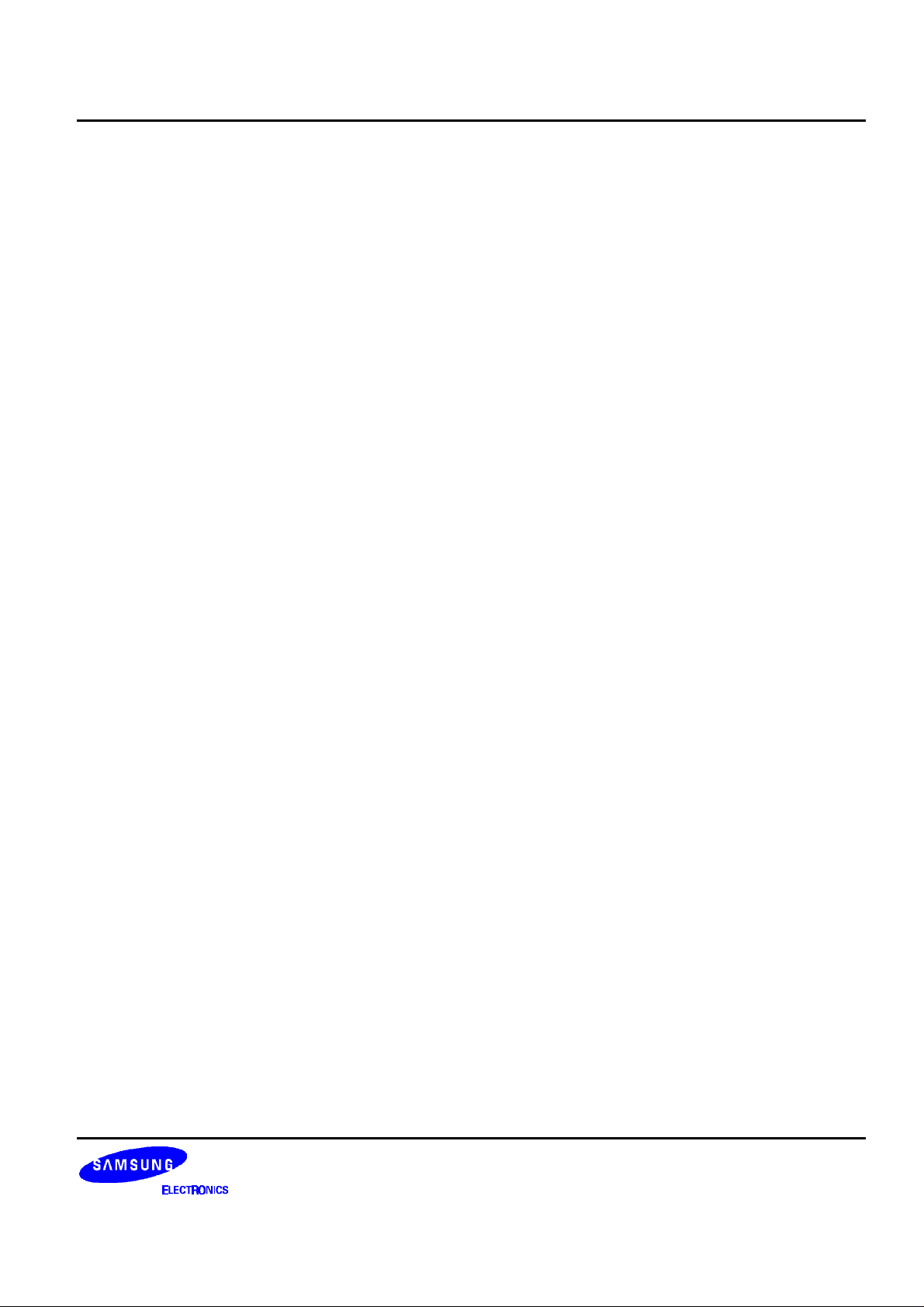
PIN ASSIGNMENTS
COM0
COM1
COM2
COM3
SEG0
SEG1
SEG2
SEG3
SEG4
SEG5
SEG6
SEG7
SEG8
64636261605958575655545352
CA
CB
VLC0
VLC1
VLC2
P0.0/ExtRef
SDAT/P0.1
SCLK/P0.2
VDD/VDD
VSS/VSS
XOUT
XIN
VPP/TEST
XTIN
XTOUT
RESETRESET/RESET
P2.0/INT0
P2.1/INT1
P2.2/TCL0
1
2
3
4
5
6
7
8
9
10
11
12
13
14
15
16
17
18
19
S3C72H8
(TOP VIEW)
51
50
43
48
47
46
45
44
43
42
41
40
39
38
37
36
35
34
33
SEG9
SEG10
SEG11
SEG12
SEG13
SEG14
SEG15
SEG16
SEG17
SEG18
SEG19
SEG20
SEG21
SEG22
SEG23
SEG24
SEG25
P5.1/C1N
P5.0/C1P
20212223242526272829303132
P2.3/FCL
P3.1/BTCO
P3.0/TCLO0
P6.0/KS0
P3.3/BUZ
P3.2/CLO
P6.1/KS1
P6.2/KS2
P6.3/KS3
P4.0/C0P
P4.1/C0N
P4.2/C0OUT
P4.3PC1OUT
Figure 1-2. S3C72H8 Pin Assignment Diagram
1-4
S3C72H8/P72H8 PRODUCT OVERVIEW
PIN DESCRIPTIONS
Table 1-1. S3C72H8 Pin Descriptions
Pin Name Pin
Type
P0.0
I/O 3-bit I/O port.
P0.1
P0.2
1-bit and 4-bit read/write and test is possible.
Port 0 is software configurable as input or output. 3-bit
Description Number
(64-QFP)
6
7
8
Share
Pin
ExtRef
–
–
Circuit
Type
D-1
pull-up resistors are software assignable.
P2.0
P2.1
P2.2
P2.3
P3.0
P3.1
P3.2
P3.3
P4.0-P4.3
P5.0-P5.1
I/O 4-bit I/O port.
1-bit and 4-bit read/write and test is possible.
Individual pins are software configurable as input or
output. 4-bit pull-up resistors are software assignable.
I/O Same as port 2.
Ports 2 and 3 can be addressed by 1, 4, and 8-bit
read/write and test instruction.
I/O 4/2-bit I/O ports. N-channel open-drain or push-pull
output. 1, 4, and 8-bit read/write and test is possible.
Ports 4 and 5 can be paired to support 8-bit data
transfer. Pull-up resistors are assignable to port unit by
software control.
17
18
19
20
21
22
23
24
29-32
33-34
INT0
INT1
TCL0
FCL
TCLO0
BTCO
CLO
BUZ
C0P/
C0N/
C0OUT/
C1OUT
C1P/
D-1
D-1
E-1
C1N
P6.0-P6.3 I/O 4-bit I/O ports. Port 6 pins are individually software
25-28 KS0-KS3 D-1
configurable as input or output. 1-bit and 4-bit read/write
and test is possible. 4-bit pull-up resistors are software
assignable.
BTCO I/O Basic timer clock output 22 P3.1 D-1
CLO I/O CPU clock output 23 P3.2 D-1
BUZ I/O 2, 4, 8 or 16 kHz frequency output for buzzer sound with
24 P3.3 D-1
4.19MHz main-system clock or 32.768 kHz sub-system
clock.
X
OUT
, X
IN
– Crystal, ceramic, or RC oscillator signal for main-
11, 12 – –
system clock. (For external clock input, use XIN and
input XIN’s reverse phase to X
XT
XT
OUT
IN
,
– Crystal oscillator signal for sub-system clock.
(For external clock input, use XTIN and input XTIN’s
reverse phase to XT
OUT
)
INT0, INT1 I/O External interrupts. The triggering edge for INT0 and
OUT
)
14, 15 – –
17, 18 P2.0, P2.1 D-1
Int1 is selectable. Only INT0 is synchronized with the
system clock.
1-5
PRODUCT OVERVIEW S3C72H8/P72H8
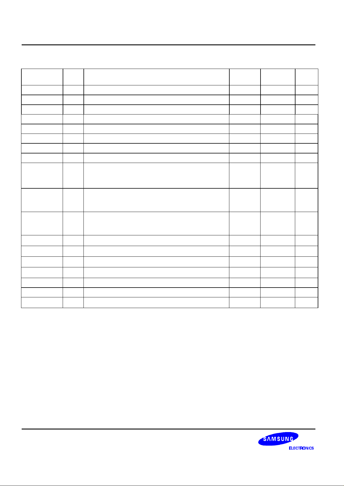
Table 1-1. S3C72H8 Pin Descriptions (Continued)
Pin Name Pin
Type
Description Number
(64-QFP)
Share
Pin
Circuit
Type
KS0-KS3 I/O Quasi-interrupt input with falling edge detection 25-28 P6.0-P6.3 D-1
ExtRef I/O External Reference input 6 P0.0 D-1
TCL0 I/O External clock input for timer/counter 0 19 P2.2 D-1
FCL I/O External clock input for frequency counter 20 P2.3 D-1
TCLO0 I/O Timer/counter 0 clock output 21 P3.0 D-1
COM0-COM3 O LCD common signal output 61-64 – H-16
SEG0-SEG25 O LCD segment output 35-60 – H-16
CA, CB – Voltage booster capacitor pins 1, 2 – –
V
LC0-VLC2
Voltage booster output pins (V
–
output, V
is the 2* V
LC1
output, V
LC0
is the regulated
LC0
is the 3* V
LC2
3-5 – –
LC0
output)
C0P, C0N,
C0OUT
I/O Comparator 0 non-inverting input, inverting input and
output. C0Out can be configured as C-MOS push-pull
29-31 P4.0-P4.2 –
or N-Ch open drain output
C1P, C1N,
C1OUT
I/OIComparator 1 non-inverting input, inverting input and
output. C1Out can be configured as C-MOS push-pull
32-34 P4.3-P5.1 –
or N-Ch open drain output
RESET
V
DD
V
SS
TEST –
– Reset signal for chip initialization 16 – B
– Main power supply 9 – –
– Ground 10 – –
Test signal input (must be connected to VSS)
13
V
PP
–
SDAT I/O Serial data for OTP programming 7 P0.1
SCLK I/O Serial clock for OTP programming 8 P0.2
V
PP
– Power supply pin for EPROM cell writing 13 TEST
NOTE: Pull-up resistors for ports 0, 2, 3, and 6 are automatically disabled if they are configured to output mode.
But pull-up resistors for ports 4 and 5 are retained its state even though they are configured to output mode.
1-6
S3C72H8/P72H8 PRODUCT OVERVIEW
PIN CIRCUIT DIAGRAMS
VDD
VDD
P-Channel
In
Data
Output
Disable
N-Channel
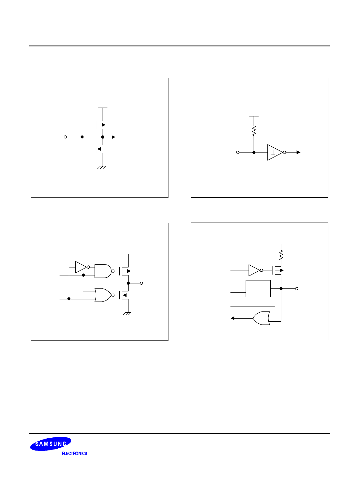
Figure 1-3. Pin Circuit Type A
VDD
P-Channel
N-Channel
Out
In
Figure 1-4. Pin Circuit Type B (Reset)
VDD
Pull-up
Resistor
Resistor
Enable
Data
Output
Disable
Input
Disable
Circuit
Type C
P-Cannel
I/O
Figure 1-5. Pin Circuit Type C
Figure 1-6. Pin Circuit Type D-1 (P0, P2, P3, P6)
1-7

PRODUCT OVERVIEW S3C72H8/P72H8
V
DD
Data
Output
Disable
Input
Disable
To Data Bus
To Comparator
VLC2
PNE
V
DD
Figure 1-7. Pin Circuit Type E-1 (P4, P5)
Pull-up
Enable
In/Out
VLC1
SEG/COM
Out
DATA
VLC0
Figure 1-8. Pin Circuit Type H-16 (COM/SEG)
1-8
 Loading...