

Page 1
9. Flow Chart of Troubleshooting
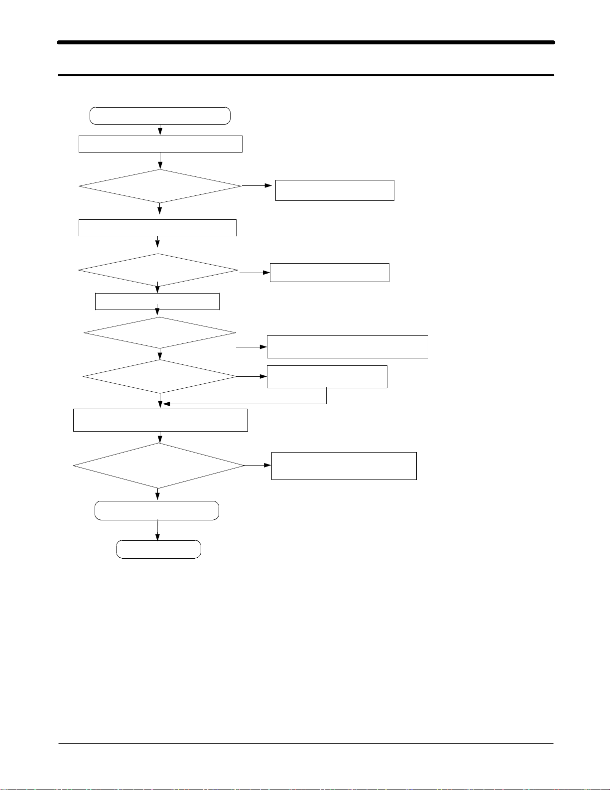
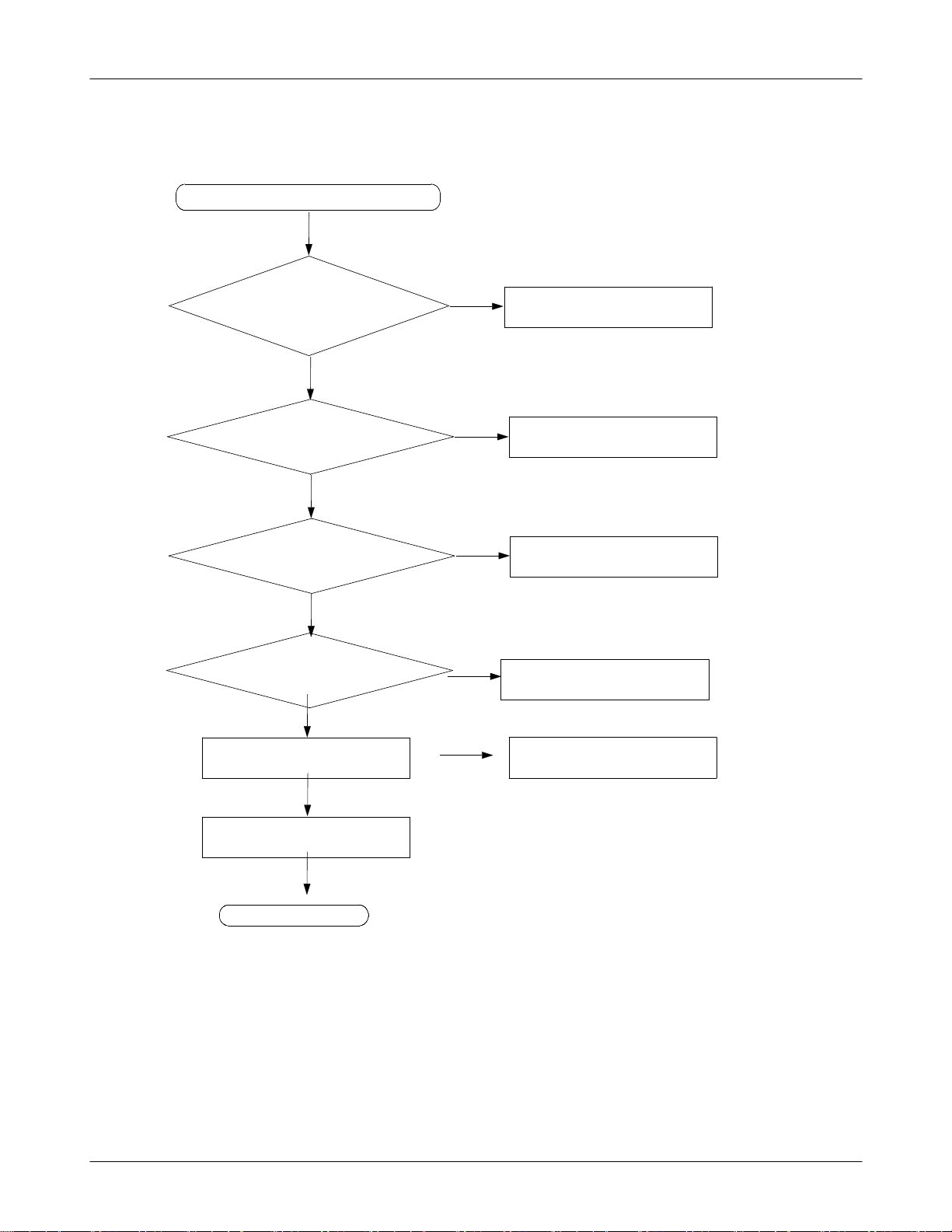
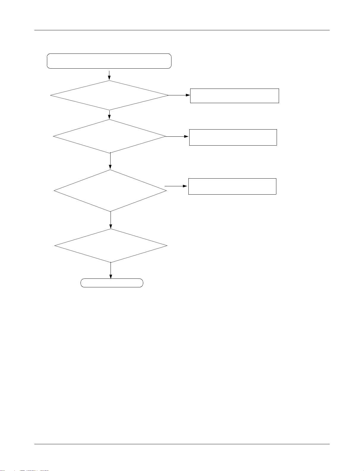
9-1-1.
Power ON
Power On' does not work
'
Check the current consumption
Yes
Current consumption
Check the Vbat Voltage
Voltage
Check the pin of PMIC400
Pin#J12
Pin#A11
P
>= 100
Pin#B7
in#B7
mA
Yes
>=3.3V
Yes
:3.0V
:1.8V
Yes
=1.3V
=1.2V
Yes
No
No
No
Check PMIC400 and L402, L404
No
Yes
Download again
Charge the Battery
Check PMIC400 and C413, C444, L403
Check the clock signal at pin#C5 of PMIC400
Freq
=
32.768khz
Yes
Check the initial operation
END
No
Check the clock generation circuit
relatedtoOSC
(
400)
9-1
SAMSUNG Proprietary-Contents may change without notice
This Document can not be used without Samsung's authorization
Page 2
Flow Chart of Troubleshooting
C
4
4
5
C
4
4
4
6
4
4
C
C447
D
4
0
1
OSC802
5
0
1
C
C
C
C
4
4
4
2
1
1
3
9
5
C401
4
5
4
L402
L403
L405
L406
C
C
C
8
2
4
4
0
0
0
4
4
4
0
9
C
R
C406
4
5
3
C
4
4
3
C
2
4
1
L404
C811
C812
C
8
0
5
C813
C
8
0
4
C
0
0
0
4
1
8
C
C
S
O
C
C
5
4
8
8
1
1
0
1
8
8
0
5
R
R
C
C
C
C
C
C
C
4
4
4
4
4
2
2
2
0
3
4
2
1
7
3
0
0
4
C
I
M
P
C414
C
2
4
5
5
4
5
C440
C436
C
AP_DI
C
4
4
4
4
2
2
2
2
7
6
5
0
0
0
L
4
4
0
0
C456
C
4
0
5
4
3
4
C
0
4
3
C
4
3
2
C
C
4
3
5
3
0
R
8
3
2
R
1
U302
4
0
3
R
4
0
6
3
9
9
1
0
8
C
R
8
4
2
0
4
7
4
0
4
C
C
C
4
1
C
4
2
9
4
0
C
R705
D
4
3
C
4
0
4
4
C
0
4
5
C
4
3
C
8
4
4
C
3
0
4
1
0
R
7
D
Z
4
0
9
R
4
R
0
5
C
4
3
1
7
3
4
C
0
0
U
0
0
4
1
R
0
7
6
0
7
R
Q
U
C
4
7
4
2
0
R
2
4
0
8
U
6
0
5
6
0
2
R
C
6
4
0
C
3
2
2
0
3
0
D
U
L
O
V
_
M
A
C
9-2
SAMSUNG Proprietary-Contents may change without notice
This Document can not be used without Samsung's authorization
Page 3
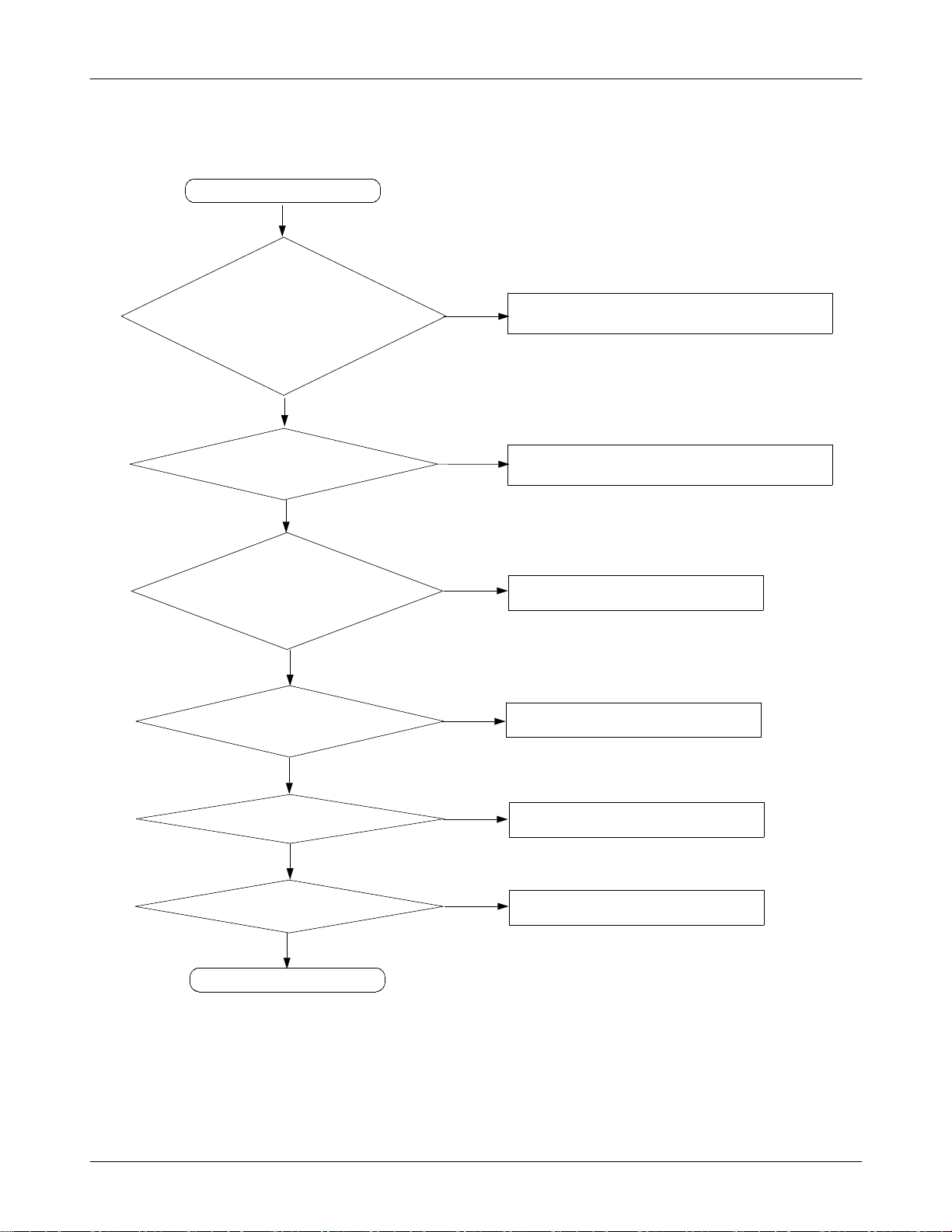
Flow Chart of Troubleshooting
9-1-2.
Initial
Initial Failure
Yes
The pin#B6 of
and
1.
V
325
the pin#B3 of
1.8V ?
Is the pin#A14 of PMIC400
Low→High"
"
PMIC400
PMIC400
Yes
?
Yes
=
No
=
No
if it has some problem, it is to be replaced.)
(
if it has some problem, it is to be replaced.)
(
Check the PMIC400
Check the PMIC400
There is
forms at the
The voltage is"High" at the
C415,
LCD display is O.K
Sound is O.K
32.768
C416,
kHz wave
C436
Yes
C426, C427
Yes
Yes
END
and
Yes
C440
No
Check the OSC400
No
Check the PMIC400
No
Check the LCD part
No
Check the Audio part
9-3
SAMSUNG Proprietary-Contents may change without notice
This Document can not be used without Samsung's authorization
Page 4
Flow Chart of Troubleshooting
9-4
SAMSUNG Proprietary-Contents may change without notice
This Document can not be used without Samsung's authorization
Page 5
Flow Chart of Troubleshooting
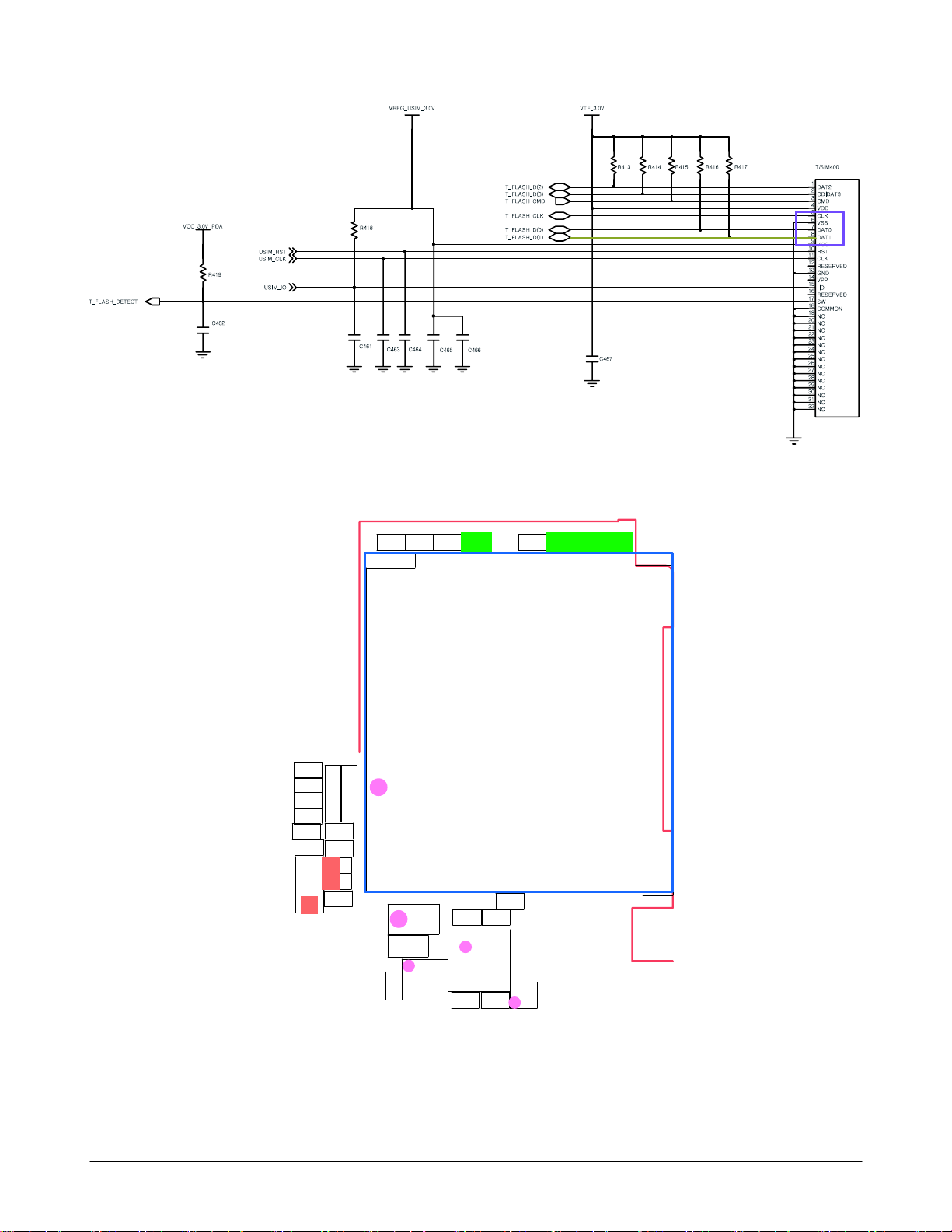
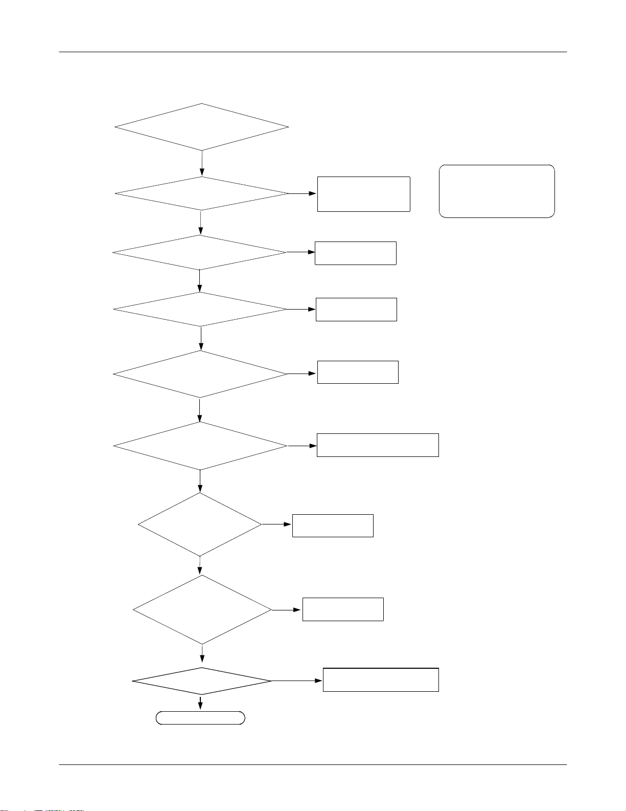
9-1-3.
Sim Part
Insert SIM is displayed on the LCD
"
Yes
Check the SIM connector's
T/SIM
(
pin#9,
Is there any signals
connection to
400)
SIM card
Yes
Is there any signals
only pin#10,#11 of
#10,#11
T/SIM
of T/SIM
Yes
400 ?
400 ?
No
No
No
Resolder or change T/SIM
Check the HEA601
Check the U605
400
Yes
Check the voltage at pin#9
of T/SIM
400 >= 2.8V ?
Yes
Is there any signals
only pin#11 of T/SIM
Check the U702
END
400 ?
Yes
Yes
No
Check the PMIC201
No
Check theUCP300
9-5
SAMSUNG Proprietary-Contents may change without notice
This Document can not be used without Samsung's authorization
Page 6
Flow Chart of Troubleshooting
4
6
2
4
1
C
9
R
C467
1
4
6
C
4
6
6
C
C465
4
6
4
C
C463
T/SIM400
4
1
0
C
R
R
4
4
1
1
4
7
4
1
6
C
4
1
7
C
R
R
4
4
1
1
5
3
4
1
8
C
1
6
4
R
4
1
1
C
5
1
2
R
R513
5
0
0
D
Z
Z
5
0
1
D
Z
D
7
0
4
7
1
3
C
C712
5
3
4
C
5
3
5
C
8
U
5
0
7
2
8
5
1
6
R
4
1
R
R509
5
0
6
U
5
C
U509
C527
9-6
SAMSUNG Proprietary-Contents may change without notice
This Document can not be used without Samsung's authorization
Page 7
Flow Chart of Troubleshooting
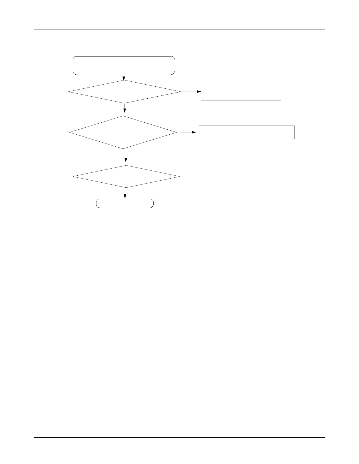
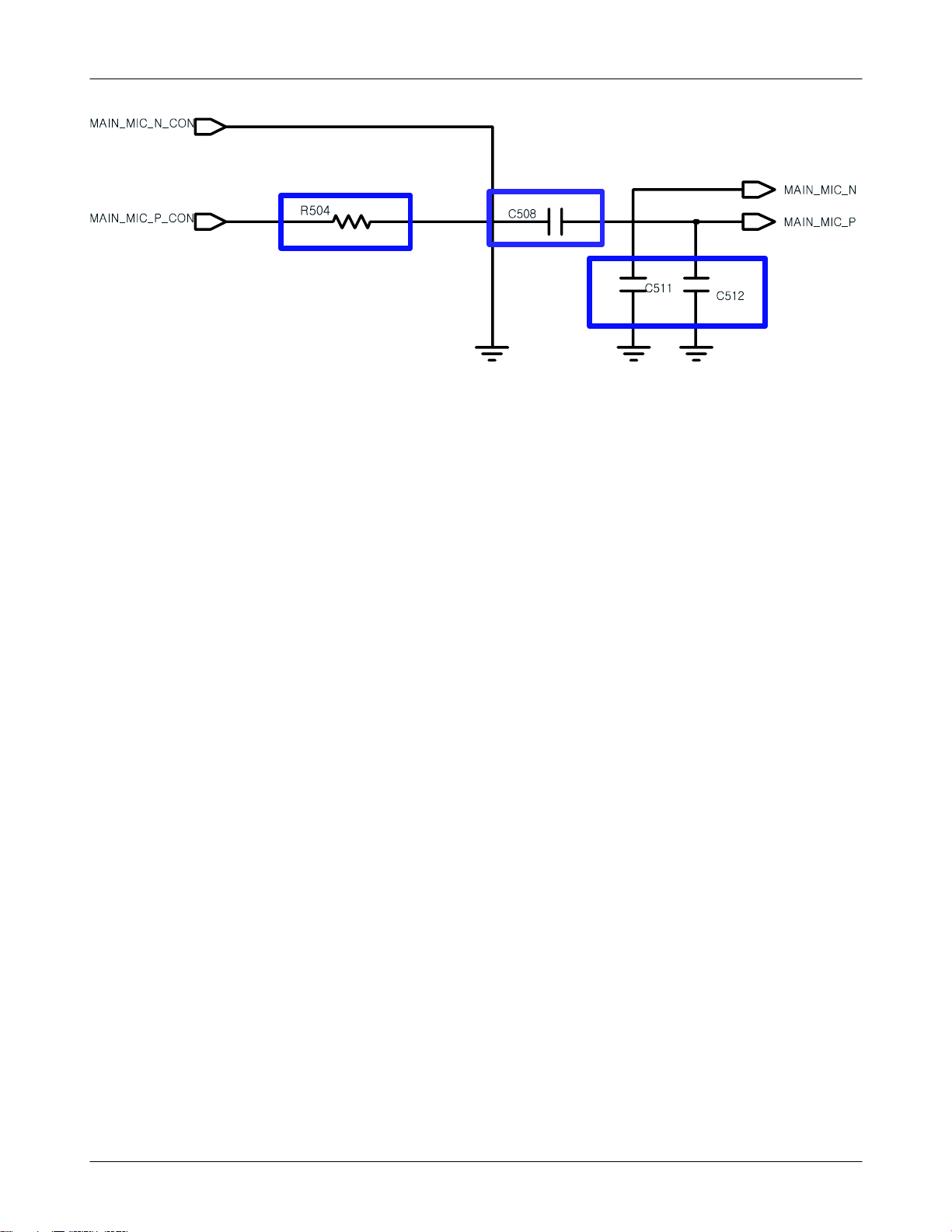
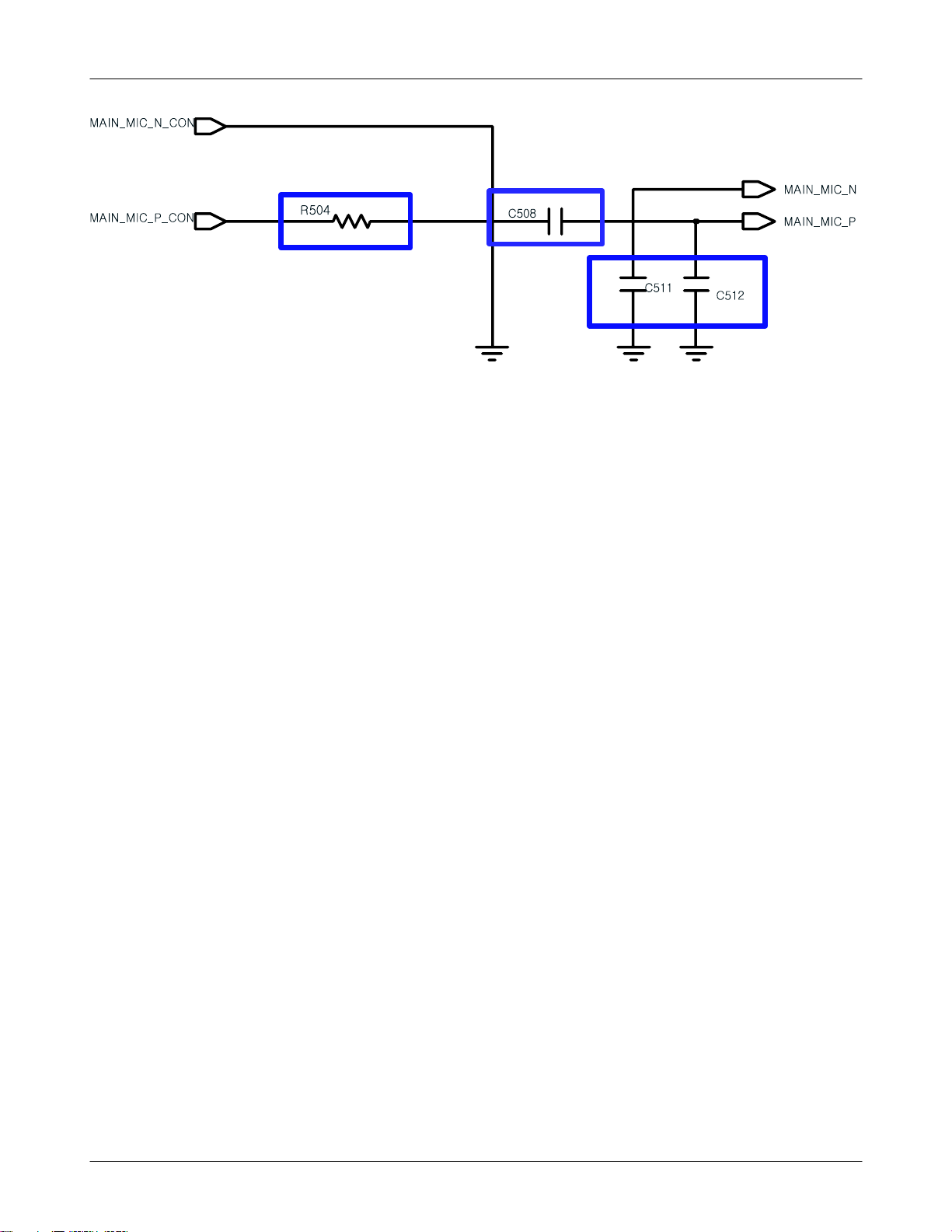
9-1-4.
MAIN Microphone Part
Check main microphone function in voice call
receiver mode
No
Check the Voltage at
L613
=1.8V
Yes
Check component soldering
status at
R504, C508, C511 and
Change the Send-end key
C512
Yes
FPCB ass'y
Yes
END
No
Resolder or change UCP300
No
Resolder or change the components
9-7
SAMSUNG Proprietary-Contents may change without notice
This Document can not be used without Samsung's authorization
Page 8
Flow Chart of Troubleshooting
9-8
SAMSUNG Proprietary-Contents may change without notice
This Document can not be used without Samsung's authorization
Page 9
Flow Chart of Troubleshooting
9-1-5.
Sub Microphone
Check sub microphone function in voice call loud mode
No
Check the connection status
of HEA602
Yes
Check voltage level at
C610
=2.6V
Yes
Check component soldering
R500,R501,R505,C500,C501,
C502,C504,C505,L506 and
status at
L508
Yes
No
Reconnect the HEA602
No
Resolder or change PMIC400
No
Resolder or change the components
Check the connection status
of HEA602
Yes
END
9-9
SAMSUNG Proprietary-Contents may change without notice
This Document can not be used without Samsung's authorization
Page 10
Flow Chart of Troubleshooting
9-10
SAMSUNG Proprietary-Contents may change without notice
This Document can not be used without Samsung's authorization
Page 11

Flow Chart of Troubleshooting
9-1-6.
SPK Part
Check speaker function.
Play MP3 with maximum volume level.
Check the signal output of
TP400,TP401,TP403..
Check the signal output of
C286 and C287.
Check the signal signal
output of C602 and C603.
Check the connection of
HEA601
No
Yes
Yes
Yes
No
No
No
Resolder or change UCP701
Check component soldering
U400,C404,C408,C409,C418,
Resolder or change the components.
Reconnect HEA601
status at
C421,C422
NO
Yes
Replace the speaker module.
Yes
End
9-11
SAMSUNG Proprietary-Contents may change without notice
This Document can not be used without Samsung's authorization
Page 12

Flow Chart of Troubleshooting
9-1-7.
Receiver Part
Check receiver function in
voice call receiver mode
Check the signal of V400
and V401.
Is the signal phase reversed?
Check the signal of pin
and#7at U403.
Is the signal phase reversed
and DC bias
Check the signal output of
C267 and C279?
Yes
Yes
=1.2
Yes
Yes
V?
No
Resolder or change U403
#5
No
Resolder or change U400
No
Resolder or change UCP300
Replace the Earjack-SubMic-
Receiver ass'y
Yes
End
9-12
SAMSUNG Proprietary-Contents may change without notice
This Document can not be used without Samsung's authorization
Page 13

9-2.
9-2-1.
RF
GSM
850
RX
NORMAL CONDITION
catch the channel?
U104 CHECK
pin
Check the Voltage at
C111
2≤-65
=2.8V?
dBm
YES
NO
?
YES
NO
No
U205, C111, C117
resolder or change
CHECK soldered
RFS100, C102, L100
Flow Chart of Troubleshooting
CONTINUOUS RX ON
RF INPUT
AMP
:-50
: 190
dBm
CH
U104 CHECK
pin
12,13≥-65
Check component
soldering status at L129,
L130, L104
C112
{
C148
&{
pin2of U100
freq
YES
U100
=2.1V?}
=2.7V?}
YES
CHECK
MHz
:19.2
YES
dBm
YES
?
?
NO
NO
resolder or change
NO
resolder or change
NO
OSC
change or resolder
U104
L129, L130, L104
PMIC400
resolder or change
100
U100
pin
13,14
: 120mV?
YES
GSM850 Receiver is O.K?
YES
END
NO
NO UCP300
U100
resolder or change
resolder or change
9-13
SAMSUNG Proprietary-Contents may change without notice
This Document can not be used without Samsung's authorization
Page 14
Flow Chart of Troubleshooting
9-2-2.
GSM
900
RX
NORMAL CONDITION
catch the channel?
NO
U104 CHECK
pin
Check the Voltage at
C111
pin
14,15≥-65
Check component
soldering status at L105,
dBm
2≤-65
=2.8V?
YES
U104 CHECK
L106, L107
dBm
YES
?
YES
No
NO
NO
?
NO
CHECK soldered
RFS100, C102, L100
U205, C111, C117
resolder or change
U104
resolder or change
L105, L106, L107
resolder or change
CONTINUOUS RX ON
RF INPUT
AMP
:-50
:37
dBm
CH
YES
U100
C112
{
=2.1V?}
C148
&{
GSM900 Receiver is O.K?
=2.7V?}
U100 CHECK
pin
2
freq
MHz
:19.2
U100
pin
13,14
: 120mV?
YES
YES
END
YES
?
YES
NO
resolder or change
NO
NO
NO UCP300
OSC
change or resolder
100
U100
resolder or change
resolder or change
PMIC400
9-14
SAMSUNG Proprietary-Contents may change without notice
This Document can not be used without Samsung's authorization
Page 15

Flow Chart of Troubleshooting
9-2-3.
DCS RX
NORMAL CONDITION
catch the channel?
NO
U104 CHECK
pin
Check the Voltage at
C111
pin
16,17≥-65
Check component
soldering status at L127,
dBm
2≤-65
=2.8V?
YES
U104 CHECK
L128, L108
dBm
YES
?
YES
?
NO
NO
NO
No
U205, C111, C117
resolder or change
CHECK soldered
RFS100, C102, L100
U104
resolder or change
L127, L128, L108
resolder or change
CONTINUOUS RX ON
RF INPUT
AMP
:-50
: 698
dBm
CH
YES
U100
C112
{
=2.1V?}
C148
&{
DCS Receiver is O.K?
CHECK
U100 pin
freq
:19.2
pin
: 120mV?
=2.7V?}
YES
2
MHz
YES
U100
15,16
YES
YES
END
?
NO
resolder or change
NO
NO
NO UCP300
OSC
change or resolder
100
U100
resolder or change
resolder or change
PMIC400
9-15
SAMSUNG Proprietary-Contents may change without notice
This Document can not be used without Samsung's authorization
Page 16

Flow Chart of Troubleshooting
9-2-4.
PCS RX
NORMAL CONDITION
catch the channel?
NO
U104 CHECK
pin
Check the Voltage at
C111
pin
16,17≥-65
Check component
soldering status at L127,
dBm
2≤-65
=2.8V?
YES
U104 CHECK
L128, L108
dBm
YES
?
YES
?
NO
NO
NO
No
U205, C111, C117
resolder or change
CHECK soldered
RFS100, C102, L100
U104
resolder or change
L127, L128, L108
resolder or change
CONTINUOUS RX ON
RF INPUT
AMP
:-50
: 661
dBm
CH
YES
U100
C112
{
=2.1V?}
C148
&{
PCS Receiver is O.K?
=2.7V?}
U100 CHECK
pin
2
freq
MHz
:19.2
U100
pin
15,16
: 120mV?
YES
YES
END
YES
?
YES
NO
NO
NO
NO
resolder or change
OSC
change or resolder
100
U100
resolder or change
resolder or change
PMIC400
UCP300
9-16
SAMSUNG Proprietary-Contents may change without notice
This Document can not be used without Samsung's authorization
Page 17

Flow Chart of Troubleshooting
9-2-5.
WCDMA Band1 Rx
NORMAL CONDITION
catch the channel?
U104 CHECK
pin
2≤-65
Check the Voltage at
C111
=2.8V?
U104 CHECK
pin
22≥-65
U100 CHECK
pin
36≥-65
dBm
YES
dBm
YES
dBm
NO
?
YES
No
NO
NO
?
NO
?
CHECK soldered
RFS100, C102, L100
U205, C111, C117
resolder or change
U104
resolder or change
C166, C169, DUF100,
R107, L116, C172
resolder or change
CONTINUOUS RX ON
RF INPUT
AMP
:-50
: 661
dBm
CH
YES
U100
C112
{
=2.1V?}
C148
&{
W2100 Receiver is O.K?
=2.7V?}
U100 CHECK
pin
2
freq
MHz
:19.2
U100
pin
29,30
: 120mV?
YES
YES
END
YES
?
YES
NO
NO
NO
NO
resolder or change
OSC
change or resolder
100
U100
resolder or change
resolder or change
9-17
PMIC400
UCP300
SAMSUNG Proprietary-Contents may change without notice
This Document can not be used without Samsung's authorization
Page 18

Flow Chart of Troubleshooting
9-2-6.
WCDMA Band8 Rx
NORMAL CONDITION
catch the channel?
U104 CHECK
pin
2≤-65
Check the Voltage at
C111
=2.8V?
U104 CHECK
pin
21≥-65
U100 CHECK
pin
30,31≥-65
dBm
YES
dBm
YES
NO
dBm
?
YES
No
NO
NO
?
NO
?
CHECK soldered
RFS100, C102, L100
U205, C111, C117
resolder or change
U104
resolder or change
C184, DUF101,C188,
C191, L122
resolder or change
CONTINUOUS RX ON
RF INPUT
AMP
:-50
: 661
dBm
CH
YES
U100
C112
{
=2.1V?}
C148
&{
W900 Receiver is O.K?
=2.7V?}
YES
RFT100 CHECK
pin
2
freq
MHz
:19.2
YES
RFT100
pin
15,16
: 120mV?
YES
YES
END
?
NO
NO
NO
NO
resolder or change
OSC
change or resolder
100
RFT100
resolder or change
resolder or change
9-18
PMIC400
UCP300
SAMSUNG Proprietary-Contents may change without notice
This Document can not be used without Samsung's authorization
Page 19

Flow Chart of Troubleshooting
9-2-7.
GSM
850
U104 pin
about
2~3
RFS
100,
check&change
NO
TX
2:
dBm?
YES
L100,C102
about
about
pin
4 : 3.8V ?
U105 pin
L117
:30
U105
:-5
NO
YES
dBm
dBm
CONTINOUS TX ON CONDITION
TX POWER DAC:
NO
8
?
C111
YES
NO
YES
V?
:2.8
YES
U104
change or resolder
Check
DC bias
U105
change or resolder
NO
U205
check&change
REF LEV.
RBW
VBW
SPAN
ATT.
CH
600
:62
: 100
:100
:10
:20
CODE APPLIED
KHz
KHz
MHz
dBm
:10
dB
NO
U100 pin
about
C112
{
&{
C148
:-5
NO
U100
=2.1V?}
=2.7V?}
dBm
55
YES
NO
YES
U100 CHECK
pin
2
freq
:19.2
MHz
?
YES
U100
pin
63,64
: 120mV?
YES
GSM850 Tranceiver is O.K?
C115, R113, R109,
R114
change or resolder
PMIC400
resolder or change
NO
NO
NO
OSC
change or resolder
100
U100
resolder or change
resolder or change
UCP300
YES
END
9-19
SAMSUNG Proprietary-Contents may change without notice
This Document can not be used without Samsung's authorization
Page 20

Flow Chart of Troubleshooting
9-2-8.
GSM
900
U104 pin
about
2~3
RFS
100,
check&change
NO
TX
2:
dBm?
YES
L100,C102
about
about
pin
4 : 3.8V ?
U105 pin
L117
:30
U104
:-5
NO
YES
dBm
dBm
NO
8
?
C111
YES
NO
YES
V?
:2.8
YES
U104
change or resolder
Check
DC bias
U104
change or resolder
NO
U205
check&change
NO
U100 pin
55
about
dBm
:-5
NO
&{
C112
{
C148
U100
=2.1V?}
NO
=2.7V?}
YES
U100 CHECK
pin
2
freq
:19.2
MHz
?
YES
U100
pin
65,66
: 120mV?
YES
GSM Receiver is O.K?
C115, R113, R109,
YES
change or resolder
PMIC400
resolder or change
NO
R114
change or resolder
NO
NO
OSC
100
U100
resolder or change
UCP300
resolder or change
YES
END
9-20
SAMSUNG Proprietary-Contents may change without notice
This Document can not be used without Samsung's authorization
Page 21

Flow Chart of Troubleshooting
9-2-9.
DCS TX
U104 pin
about
2~3
RFS
100,
check&change
NO
2:
dBm?
YES
L100,C102
about
about
pin
4 : 3.8V ?
U105 pin
L118
:30
U105
:-5
NO
YES
dBm
dBm
NO
1
?
C111
YES
NO
YES
V?
:2.8
YES
U104
change or resolder
Check
DC bias
U105
change or resolder
NO
U205
check&change
NO
U100 pin
56
about
dBm
:-5
NO
&{
C112
{
C148
U100
=2.1V?}
NO
=2.7V?}
YES
U100 CHECK
pin
2
freq
:19.2
MHz
?
YES
U100
pin
63,64
: 120mV?
YES
DCS Receiver is O.K?
C110, R113, R109,
YES
change or resolder
PMIC400
resolder or change
NO
R114
change or resolder
NO
NO
OSC
100
U100
resolder or change
UCP300
resolder or change
YES
END
9-21
SAMSUNG Proprietary-Contents may change without notice
This Document can not be used without Samsung's authorization
Page 22

Flow Chart of Troubleshooting
9-2-10.
PCS TX
U104 pin
about
2~3
RFS
L100,C102
100,
check&change
NO
dBm?
YES
2:
about
pin
U105 pin
about
L118
dBm
:30
NO
U105
4 : 3.8V ?
YES
dBm
:-5
NO
1
?
C111
YES
NO
YES
V?
:2.8
YES
U104
change or resolder
Check
DC bias
U105
change or resolder
NO
U205
check&change
NO
U100 pin
56
about
dBm
:-5
NO
&{
C112
{
C148
U100
=2.1V?}
NO
=2.7V?}
YES
U100 CHECK
pin
2
freq
:19.2
MHz
?
YES
U100
pin
63,64
: 120mV?
YES
PCS Receiver is O.K?
C110, R110, R111,
YES
change or resolder
PMIC400
resolder or change
NO
R112
change or resolder
NO
NO
OSC
100
U100
resolder or change
UCP300
resolder or change
YES
END
9-22
SAMSUNG Proprietary-Contents may change without notice
This Document can not be used without Samsung's authorization
Page 23

Flow Chart of Troubleshooting
9-2-11.
WCDMA Band1 TX
C166
:20
C171
:20
L115
:-5
NO
dBm
NO
dBm
dBm
U104 pin
about
2~3
RFS
100,
check&change
2:
dBm?
YES
L100,C102
about
about
about
C111
YES
change or resolder
C171, C174, DUF100,
YES
change or resolder
YES
change or resolder
V?
:2.8
YES
U104
C166, C169
PAM100
NO
U205
check&change
NO
dBm
:-5
NO
=2.1V?}
=2.7V?}
YES
NO
&{
about
C112
{
C108
U100
C148
YES
U100 CHECK
pin
2
freq
:19.2
MHz
?
YES
U100
pin
63,64
: 120mV?
YES
W2100 Transmitter is O.K?
C108, L114, F101,
C165, L115
resolder or change
PMIC400
resolder or change
NO
NO
OSC
change or resolder
resolder or change
NO
100
U100
UCP300
resolder or change
YES
END
9-23
SAMSUNG Proprietary-Contents may change without notice
This Document can not be used without Samsung's authorization
Page 24

Flow Chart of Troubleshooting
9-2-11.
WCDMA Band8 TX
C184
:20
L121
:20
L115
:-5
NO
dBm
NO
dBm
dBm
U104 pin
about
2~3
RFS
100,
check&change
2:
dBm?
YES
L100,C102
about
about
about
C111
YES
YES
YES
V?
:2.8
YES
U104
change or resolder
L121, C190, CPL100,
DUF101, C184
change or resolder
PAM102
change or resolder
NO
U205
check&change
NO
dBm
:-5
NO
=2.1V?}
=2.7V?}
YES
NO
&{
about
C112
{
C109
U100
C148
YES
U100 CHECK
pin
2
freq
:19.2
MHz
?
YES
U100
pin
63,64
: 120mV?
YES
W900 Transmitter is O.K?
C109, L124, C194,
F102, C125, C193
resolder or change
PMIC400
resolder or change
NO
NO
NO
OSC
change or resolder
100
U100
resolder or change
resolder or change
UCP300
YES
END
9-24
SAMSUNG Proprietary-Contents may change without notice
This Document can not be used without Samsung's authorization
Page 25

Flow Chart of Troubleshooting
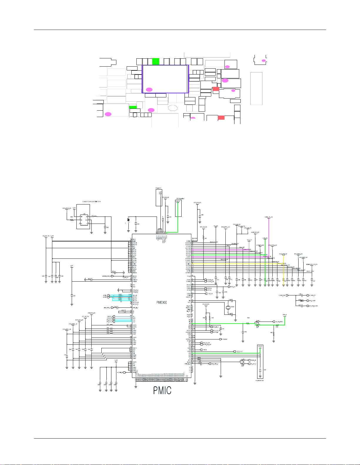
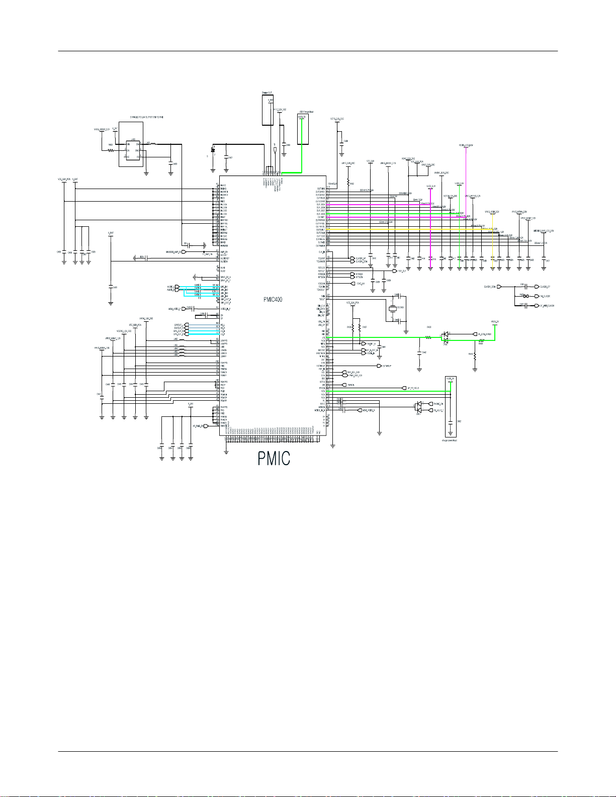
9-3.
Bluetooth
Check BT function
ON
Yes
Check the Voltage at
C218
=3.0V
Yes
Check26MHz clock at
C202 point
Yes
Check the Voltage of
L207
=1.5V
Yes
Check the status
at C204
No
Enable BT function
No
Check PMIC400
No
Check OSC200
No
Resolder or change L207
No
Resolder or Replace C204
END
Yes
9-25
SAMSUNG Proprietary-Contents may change without notice
This Document can not be used without Samsung's authorization
Page 26

Flow Chart of Troubleshooting
1
C458
S
O
1
0
1
R
P
C109
R114
C169
R
0
0
1
A
T
R
1
1
6
C123
1
0
8
C
1
1
9
R
1
1
5
1
0
M
A
C208
R204
L
2
0
1
0
6
2
R
2
0
7
R
2
0
8
R
2
0
9
R
2
0
5
R
1
1
2
R
2
1
0
R
2
0
7
C
C
2
1
3
2
1
5
C
C205
0
3
U
C
C
2
2
0
1
9
0
U
2
0
4
9-26
SAMSUNG Proprietary-Contents may change without notice
This Document can not be used without Samsung's authorization
U300
C302
3
0
1
C
2
1
2
C
C
2
1
8
Page 27

Flow Chart of Troubleshooting
9-4.
FM Radio Part
FM Radio does not work
Yes
Check the connection
at HEA400
Yes
Check the Audio signal
at C416, C417 and
C525
No
Yes
connect earjack to HEA400
Check the Audio signal
at C260, C262
Yes
Check the Audio signal
at L400, L401
C602, C603; SPK)
(
No
No
Check U400
Resolder L400, L401 and
check PMIC400
No
Check the
supply at C216
Check the FM RF
signal at C207
change the main PBA
3.0V
Yes
Yes
Yes
change earjack ASSY
No
Check U200
No
change earjack ASSY
9-27
SAMSUNG Proprietary-Contents may change without notice
This Document can not be used without Samsung's authorization
Page 28

Flow Chart of Troubleshooting
9-28
SAMSUNG Proprietary-Contents may change without notice
This Document can not be used without Samsung's authorization
Page 29

Block Diagrams
7.
7-1.
Main Block Diagram
7-1
SAMSUNG Proprietary-Contents may change without notice
This Document can not be used without Samsung's authorization
Page 30

Block Diagrams
7-2.
RF Solution Block Diagram
7-2
SAMSUNG Proprietary-Contents may change without notice
This Document can not be used without Samsung's authorization
Page 31

8.
Top
PCB Diagrams
8-1
Page 32
PCB Diagrams
Bottom
8-2
 Loading...