

Page 1
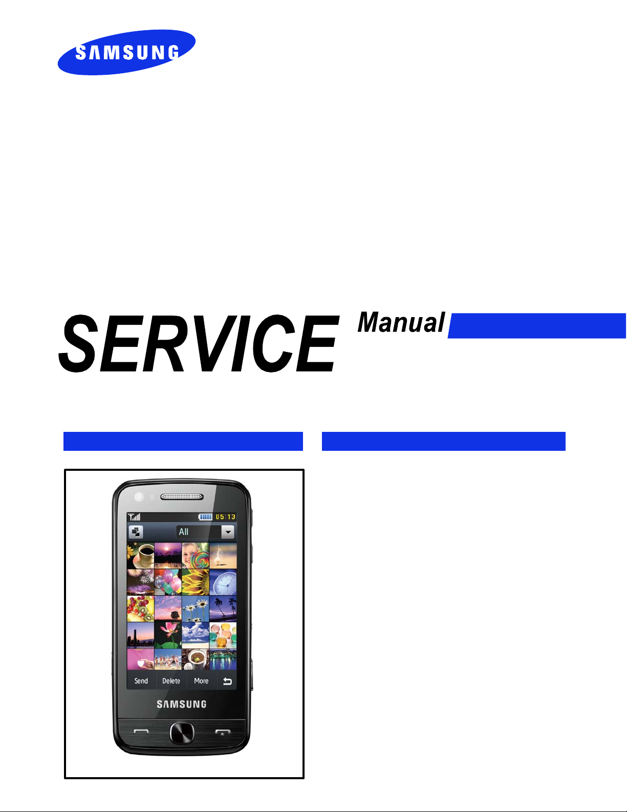
GSM TELEPHONE
GT-M8910B
efrcom
GSM TELEPHONE
CONTENTS
Safety Precautions
1.
Specification
2.
Product Function
3.
Array course control
4.
Exploded View and Parts List
5.
Main Electrical Parts List
6.
Block Diagrams
7.
PCB Diagrams
8.
Flow Chart of Troubleshooting
9.
Reference data
10.
Disassembly and Assembly
11.
instructions
Page 2
MAIN Electrical Parts List
6.
SEC CODE Design Location Description
0403-001749
0404-001172
0406-001288
0406-001288
0406-001288
0406-001288
0406-001288
0406-001288
0406-001288
0406-001288
0406-001288
0406-001288
0406-001288
0406-001288
0406-001288
0406-001288
0406-001288
0406-001288
0406-001288
0406-001288
0407-001002
0407-001002
0504-000168
0504-001138
0505-001518
0505-002088
0505-002088
0801-003016
0801-003130
0801-003200
0801-003200
0801-003265
0902-002440
1001-001408
1001-001410
1001-001481
1001-001580
1001-001581
1001-001581
1001-001599
1003-002047
1003-002169
1003-002216
1003-002216
ZD704 PZU5.6B
D300 RB520S-30
V602 PESD5V0S1UL
V603 PESD5V0S1UL
ZD500 PESD5V0S1UL
ZD501 PESD5V0S1UL
ZD600 PESD5V0S1UL
ZD601 PESD5V0S1UL
ZD602 PESD5V0S1UL
ZD603 PESD5V0S1UL
ZD604 PESD5V0S1UL
ZD605 PESD5V0S1UL
ZD606 PESD5V0S1UL
ZD607 PESD5V0S1UL
ZD608 PESD5V0S1UL
ZD700 PESD5V0S1UL
ZD701 PESD5V0S1UL
ZD702 PESD5V0S1UL
ZD703 PESD5V0S1UL
ZD705 PESD5V0S1UL
D400 DAN222TL
D401 DAN222TL
Q701 DTC144EE/TR
Q700 DTA114EM
Q600 SI1012R
Q300
Q800
U509 NC7SV08L6X
U802 NC7SV17L6X
U101 NC7SZ00L6X
U303 NC7SZ00L6X
U301
UCP800 SC36410A8N-A040
U502 NLAS3799B
U501 NLAS5223BMNR2G
U801 FSUSB42UMX
U701 FSA9480UCX
U500 FSA9480UCX
U605 NLAS3899BMNTBG
U704 STG3220QTR
U504 ISA1000
U507 A3908EEETR-T
U302 NLSX4373MUTAG
U800 NLSX4373MUTAG
SK3541
2
SK3541
2
AUP1G74GM
74
6-1
SAMSUNG Proprietary-Contents may change without notice
This Document can not be used without Samsung's authorization
Page 3

Main Electrical Parts List
SEC CODE Design Location Description
1003-002216
1201-002774
1201-002830
1201-002889
1201-002887
1201-002934
1203-004340
1203-004819
1203-004819
1203-005367
1203-005485
1203-005522
1203-005652
1203-005652
1203-005772
1203-005795
1203-005908
1203-005934
1203-005934
1204-003026
1205-003297
1205-003582
1205-003757
1209-001817
1209-001872
1404-001221
2007-000137
2007-000138
2007-000138
2007-000138
2007-000138
2007-000138
2007-000138
2007-000138
2007-000138
2007-000138
2007-000138
2007-000138
2007-000141
2007-000141
2007-000141
2007-000141
2007-000141
2007-000143
U803 NLSX4373MUTAG
U203 BGM681L11
PAM101 SKY77336-13
PAM100 SKY77186
PAM102 SKY7718
U703 FSM6151L6X-F113
U601 RP150K008A
U406 RP103K281D-TR
U407 RP103K281D-TR
U700 XC6209B502DR
U505 MIC5365-3.0YMT
U602 STOD02PUR
U603 RT8036EGQW
U604 RT8036EGQW
U300 MAX17040G-T
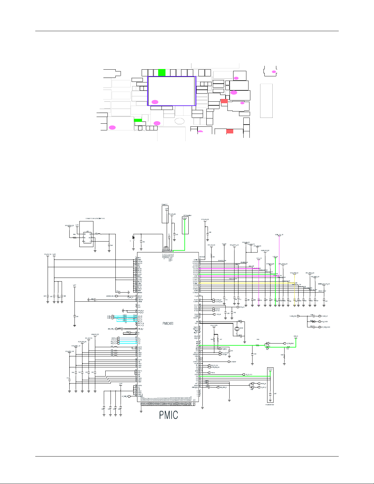
PMIC400 MAX8906EWA
U400 ISL9104AIRUFZ-T
U304 XC61CN2702NR-G
U702 XC61CN2702NR-G
U202 SI4709-B-GMR
U100 RTR6285
UCP300 MSM6290
UCP500 MAX9880
U508 BMA020
U506 AK8973B
TH300 NCP15WB473J04RC
R503 RC1005J202CS
R101 RC1005J101CS
R109 RC1005J101CS
R116 RC1005J101CS
R316 RC1005J101CS
R506 RC1005J101CS
R507 RC1005J101CS
R516 RC1005J101CS
R602 RC1005J101CS
R711 RC1005J101CS
R816 RC1005J101CS
R830 RC1005J101CS
R114 RC1005J222CS
R823 RC1005J222CS
R824 RC1005J222CS
R833 RC1005J222CS
U806 RC1005J222CS
R301 RC1005J472CS
8
6-2
SAMSUNG Proprietary-Contents may change without notice
This Document can not be used without Samsung's authorization
Page 4

Main Electrical Parts List
SEC CODE Design Location Description
2007-000143
2007-000143
2007-000143
2007-000148
2007-000148
2007-000148
2007-000148
2007-000148
2007-000148
2007-000151
2007-000151
2007-000151
2007-000153
2007-000157
2007-000157
2007-000157
2007-000157
2007-000157
2007-000162
2007-000162
2007-000162
2007-000162
2007-000170
2007-000170
2007-000170
2007-000566
2007-000932
2007-001244
2007-001290
2007-001290
2007-001290
2007-001292
2007-001292
2007-001292
2007-001294
2007-001306
2007-001306
2007-001333
2007-002796
2007-003022
2007-007014
2007-007107
2007-007107
2007-007156
R302 RC1005J472CS
R806 RC1005J472CS
R807 RC1005J472CS
R305 RC1005J103CS
R409 RC1005J103CS
R410 RC1005J103CS
R512 RC1005J103CS
R603 RC1005J103CS
R805 RC1005J103CS
R418 RC1005J153CS
R821 RC1005J153CS
R822 RC1005J153CS
R609 RC1005J223CS
R413 RC1005J473CS
R414 RC1005J473CS
R415 RC1005J473CS
R416 RC1005J473CS
R417 RC1005J473CS
R314 RC1005J104CS
R509 RC1005J104CS
R818 RC1005J104CS
R838 RC1005J104CS
R312 RC1005J105CS
R320 RC1005J105CS
R827 RC1005J105CS
R601 RC1005J224CS
R828 RC1005J471CS
R606 RC1005J913CS
R117 RC1005J240CS
R119 RC1005J240CS
R309 RC1005J240CS
R315 RC1005J330CS
R701 RC1005J330CS
R704 RC1005J330CS
R708 RC1005J360CS
R115 MCR01MZP5J151
R707 MCR01MZP5J151
R513 MCR01MZP5J183
R502 MCR01MZP5J511
R118 TSR16GJ620V
R419 MCR01MZP5J513
R310 RC1005F1003CS
R311 RC1005F1003CS
R504 RC1005J1ROCS
6-3
SAMSUNG Proprietary-Contents may change without notice
This Document can not be used without Samsung's authorization
Page 5
Main Electrical Parts List
SEC CODE Design Location Description
2007-007193
2007-007193
2007-007307
2007-007307
2007-007309
2007-007741
2007-007943
2007-007981
2007-008045
2007-008045
2007-008045
2007-008045
2007-008045
2007-008045
2007-008045
2007-008045
2007-008045
2007-008045
2007-008045
2007-008045
2007-008045
2007-008045
2007-008049
2007-008049
2007-008049
2007-008052
2007-008052
2007-008052
2007-008052
2007-008052
2007-008052
2007-008055
2007-008055
2007-008055
2007-008055
2007-008055
2007-008055
2007-008055
2007-008055
2007-008055
2007-008486
2007-008516
2007-008516
2007-008516
R111 TSR16GJ5R1V
R113 TSR16GJ5R1V
R303 RK73H1ETP1500F
R304 RK73H1ETP1500F
R102 MCR01MZP5F1202
R408 M5534204B10E0R
R705 RK73H1ETP5603F
R510 ERJ2RKF1803X
R306 ERJ1GEJ101C
R308 ERJ1GEJ101C
R321 ERJ1GEJ101C
R508 ERJ1GEJ101C
R700 ERJ1GEJ101C
R709 ERJ1GEJ101C
R710 ERJ1GEJ101C
R808 ERJ1GEJ101C
R809 ERJ1GEJ101C
R810 ERJ1GEJ101C
R840 ERJ1GEJ101C
R841 ERJ1GEJ101C
R844 ERJ1GEJ101C
R845 ERJ1GEJ101C
R307 MCR006YZPJ202
R500 MCR006YZPJ202
R505 MCR006YZPJ202
R800 ERJ1GENJ472X
R801 ERJ1GENJ472X
R812 ERJ1GENJ472X
R813 ERJ1GENJ472X
R814 ERJ1GENJ472X
R815 ERJ1GENJ472X
R108 ERJ1GENJ104X
R400 ERJ1GENJ104X
R402 ERJ1GENJ104X
R406 ERJ1GENJ104X
R407 ERJ1GENJ104X
R703 ERJ1GENJ104X
R706 ERJ1GENJ104X
R832 ERJ1GENJ104X
R839 ERJ1GENJ104X
R610 ERJ1GEJ204C
R107 ERJ1GEJ103C
R702 ERJ1GEJ103C
R803 ERJ1GEJ103C
6-4
SAMSUNG Proprietary-Contents may change without notice
This Document can not be used without Samsung's authorization
Page 6

Main Electrical Parts List
SEC CODE Design Location Description
2007-008516
2007-008516
2007-008766
2007-008806
2007-009084
2007-009084
2007-009155
2007-009171
2007-009171
2007-009171
2007-009171
2007-009171
2007-009212
2007-009793
2007-009879
2007-009879
2007-009879
2007-009879
2007-009964
2007-010030
2203-000233
2203-000233
2203-000233
2203-000254
2203-000254
2203-000254
2203-000254
2203-000254
2203-000254
2203-000254
2203-000254
2203-000254
2203-000278
2203-000278
2203-000425
2203-000425
2203-000425
2203-000438
2203-000438
2203-000489
2203-000627
2203-000628
2203-000679
2203-000679
R804 ERJ1GEJ103C
R842 ERJ1GEJ103C
R313 ERJ2RKF6041X
R112 RC0603J510CS
R811 MCR006YZPJ105
R817 MCR006YZPJ105
R611 MCR006YZPJ474
R205 MCR006YZPJ513
R206 MCR006YZPJ513
R207 MCR006YZPJ513
R208 MCR006YZPJ513
R209 MCR006YZPJ513
R110 MCR006YZPF1001
R843 MCR006YZPF3002
R103 ERJ1GEF1101C
R104 ERJ1GEF1101C
R105 ERJ1GEF1101C
R106 ERJ1GEF1101C
R826 MCR01MZP5F44R2
R820 MCR01MZP5F6491
C108 GRP1555C1H101J
C118 GRP1555C1H101J
C216 GRP1555C1H101J
C109 GRP155R71C103K
C309 GRP155R71C103K
C311 GRP155R71C103K
C318 GRP155R71C103K
C321 GRP155R71C103K
C323 GRP155R71C103K
C431 GRP155R71C103K
C437 GRP155R71C103K
C714 GRP155R71C103K
C145 GRP1555C1H100D
C509 GRP1555C1H100D
C436 GRP1555C1H180J
C440 GRP1555C1H180J
C717 GRP1555C1H180J
C313 GRP155R71H102K
C700 GRP155R71H102K
C300 GRP155R71H222K
C114 GRM1555C1H220J
C156 GRP1555C1H220JZ01E
C632 GRP1555C1H270J
C821 GRP1555C1H270J
6-5
SAMSUNG Proprietary-Contents may change without notice
This Document can not be used without Samsung's authorization
Page 7

Main Electrical Parts List
SEC CODE Design Location Description
2203-000679
2203-000679
2203-000679
2203-000725
2203-000812
2203-000812
2203-000812
2203-000812
2203-000812
2203-000812
2203-000812
2203-000812
2203-000812
2203-000854
2203-000854
2203-001259
2703-002207
2203-002525
2203-002677
2203-002709
2203-005052
2203-005055
2203-005056
2203-005056
2203-005138
2203-005281
2203-005281
2203-005288
2203-005288
2203-005288
2203-005383
2203-005383
2203-005395
2203-005395
2203-005571
2203-005682
2203-005682
2203-005682
2203-005682
2203-005682
2203-005682
2203-005725
2203-005725
2203-005725
C826 GRP1555C1H270J
C827 GRP1555C1H270J
R829 GRP1555C1H270J
C526 GRP155R71H392KA01E
C110 GRP1555C1H330J
C111 GRP1555C1H330J
C163 GRP1555C1H330J
C164 GRP1555C1H330J
C179 GRP1555C1H330J
C305 GRP1555C1H330J
C501 GRP1555C1H330J
C807 GRP1555C1H330J
C810 GRP1555C1H330J
C169 GRP1555C1H390J
C825 GRP1555C1H390J
C177 GRP1555C1H8R0DZ01E
C181 CIH05T3N3SNC
C627 GRP155R71H561KD01E
R204 CL05CR75BBNC
C448 C1005Y5V1C104ZT
C200 GRP1555C1H3R3CZ01E
C165 GRP1555C1H5R6CZ01E
C651 GRP1555C1H6R8CZ01E
C652 GRP1555C1H6R8CZ01E
C828
C178 GRP1555C1H1R5BZ01E
C184 GRP1555C1H1R5BZ01E
C104 GRP1555C1H1R0BZ01E
C166 GRP1555C1H1R0BZ01E
C222 GRP1555C1H1R0BZ01E
C504 CL05C070JBNC
C505 CL05C070JBNC
C142 C1005CG1H4R7BT
C147 C1005CG1H4R7BT
C214 GJ221BF50J106ZD01L
C102 GRP0335C1E330JD01E
C121 GRP0335C1E330JD01E
C149 GRP0335C1E330JD01E
C804 GRP0335C1E330JD01E
C815 GRP0335C1E330JD01E
C816 GRP0335C1E330JD01E
C117 GRP0335C1E220JD01E
C124 GRP0335C1E220JD01E
C129 GRP0335C1E220JD01E
04025
C182KAT2A
6-6
SAMSUNG Proprietary-Contents may change without notice
This Document can not be used without Samsung's authorization
Page 8

Main Electrical Parts List
SEC CODE Design Location Description
2203-005725
2203-005725
2203-005725
2203-005725
2203-005725
2203-005725
2203-005725
2203-005725
2203-005729
2203-005729
2203-005732
2203-005732
2203-005736
2203-005736
2203-005736
2203-005736
2203-005736
2203-005736
2203-005736
2203-005736
2203-005736
2203-005806
2203-005806
2203-005806
2203-006047
2203-006048
2203-006048
2203-006048
2203-006048
2203-006048
2203-006048
2203-006048
2203-006048
2203-006048
2203-006048
2203-006048
2203-006048
2203-006048
2203-006048
2203-006048
2203-006048
2203-006048
2203-006048
2203-006048
C131 GRP0335C1E220JD01E
C132 GRP0335C1E220JD01E
C134 GRP0335C1E220JD01E
C135 GRP0335C1E220JD01E
C138 GRP0335C1E220JD01E
C141 GRP0335C1E220JD01E
C143 GRP0335C1E220JD01E
C158 GRP0335C1E220JD01E
C818 CL03C150JAGC
C819 CL03C150JAGC
C100 GRP0335C1E680JD01E
C101 GRP0335C1E680JD01E
C106 GRP0335C1E101JD01E
C115 GRP0335C1E101JD01E
C136 GRP0335C1E101JD01E
C139 GRP0335C1E101JD01E
C144 GRP0335C1E101JD01E
C150 GRP0335C1E101JD01E
C152 GRP0335C1E101JD01E
C160 GRP0335C1E101JD01E
C402 GRP0335C1E101JD01E
C122 GRP033R71C102KD01E
C128 GRP033R71C102KD01E
C137 GRP033R71C102KD01E
C304 C1005X7R1C333K
C113 GRM155R71A104K
C123 GRM155R71A104K
C204 GRM155R71A104K
C205 GRM155R71A104K
C303 GRM155R71A104K
C306 GRM155R71A104K
C310 GRM155R71A104K
C312 GRM155R71A104K
C316 GRM155R71A104K
C317 GRM155R71A104K
C320 GRM155R71A104K
C322 GRM155R71A104K
C324 GRM155R71A104K
C326 GRM155R71A104K
C327 GRM155R71A104K
C329 GRM155R71A104K
C330 GRM155R71A104K
C462 GRM155R71A104K
C465 GRM155R71A104K
6-7
SAMSUNG Proprietary-Contents may change without notice
This Document can not be used without Samsung's authorization
Page 9

Main Electrical Parts List
SEC CODE Design Location Description
2203-006048
2203-006048
2203-006048
2203-006048
2203-006048
2203-006048
2203-006048
2203-006048
2203-006048
2203-006048
2203-006048
2203-006048
2203-006048
2203-006048
2203-006048
2203-006048
2203-006048
2203-006090
2203-006123
2203-006123
2203-006137
2203-006137
2203-006137
2203-006137
2203-006194
2203-006194
2203-006399
2203-006399
2203-006399
2203-006399
2203-006399
2203-006399
2203-006399
2203-006399
2203-006399
2203-006399
2203-006399
2203-006399
2203-006399
2203-006399
2203-006399
2203-006399
2203-006399
2203-006399
C508 GRM155R71A104K
C511 GRM155R71A104K
C519 GRM155R71A104K
C522 GRM155R71A104K
C525 GRM155R71A104K
C527 GRM155R71A104K
C528 GRM155R71A104K
C532 GRM155R71A104K
C535 GRM155R71A104K
C709 GRM155R71A104K
C713 GRM155R71A104K
C715 GRM155R71A104K
C802 GRM155R71A104K
C808 GRM155R71A104K
C814 GRM155R71A104K
C820 GRM155R71A104K
C824 GRM155R71A104K
C702 GRM21BR60J106KE01L
C218 GRM0335C1E5R6CD01D
C219 GRM0335C1E5R6CD01D
C435 CL05B223KONC
C438 CL05B223KONC
C450 CL05B223KONC
C531 CL05B223KONC
C127 GRP033R70J103KA01E
C428 GRP033R70J103KA01E
C203 GRM155R60J105KE19D
C314 GRM155R60J105KE19D
C412 GRM155R60J105KE19D
C416 GRM155R60J105KE19D
C422 GRM155R60J105KE19D
C439 GRM155R60J105KE19D
C459 GRM155R60J105KE19D
C502 GRM155R60J105KE19D
C516 GRM155R60J105KE19D
C529 GRM155R60J105KE19D
C602 GRM155R60J105KE19D
C606 GRM155R60J105KE19D
C614 GRM155R60J105KE19D
C646 GRM155R60J105KE19D
C654 GRM155R60J105KE19D
C813 GRM155R60J105KE19D
C211 GRM155R60J105KE19D
C315 GRM155R60J105KE19D
6-8
SAMSUNG Proprietary-Contents may change without notice
This Document can not be used without Samsung's authorization
Page 10

Main Electrical Parts List
SEC CODE Design Location Description
2203-006399
2203-006399
2203-006399
2203-006399
2203-006399
2203-006399
2203-006399
2203-006399
2203-006399
2203-006399
2203-006399
2203-006399
2203-006399
2203-006399
2203-006399
2203-006399
2203-006399
2203-006399
2203-006399
2203-006399
2203-006399
2203-006399
2203-006399
2203-006399
2203-006399
2203-006399
2203-006399
2203-006399
2203-006399
2203-006399
2203-006399
2203-006399
2203-006399
2203-006399
2203-006399
2203-006399
2203-006399
2203-006399
2203-006399
2203-006399
2203-006399
2203-006399
2203-006399
2203-006423
C413 GRM155R60J105KE19D
C417 GRM155R60J105KE19D
C424 GRM155R60J105KE19D
C441 GRM155R60J105KE19D
C460 GRM155R60J105KE19D
C506 GRM155R60J105KE19D
C517 GRM155R60J105KE19D
C533 GRM155R60J105KE19D
C603 GRM155R60J105KE19D
C607 GRM155R60J105KE19D
C640 GRM155R60J105KE19D
C647 GRM155R60J105KE19D
C710 GRM155R60J105KE19D
C213 GRM155R60J105KE19D
C409 GRM155R60J105KE19D
C414 GRM155R60J105KE19D
C419 GRM155R60J105KE19D
C426 GRM155R60J105KE19D
C457 GRM155R60J105KE19D
C467 GRM155R60J105KE19D
C514 GRM155R60J105KE19D
C518 GRM155R60J105KE19D
C600 GRM155R60J105KE19D
C604 GRM155R60J105KE19D
C608 GRM155R60J105KE19D
C641 GRM155R60J105KE19D
C649 GRM155R60J105KE19D
C806 GRM155R60J105KE19D
C307 GRM155R60J105KE19D
C411 GRM155R60J105KE19D
C415 GRM155R60J105KE19D
C421 GRM155R60J105KE19D
C433 GRM155R60J105KE19D
C458 GRM155R60J105KE19D
C500 GRM155R60J105KE19D
C515 GRM155R60J105KE19D
C520 GRM155R60J105KE19D
C601 GRM155R60J105KE19D
C605 GRM155R60J105KE19D
C613 GRM155R60J105KE19D
C642 GRM155R60J105KE19D
C653 GRM155R60J105KE19D
C809 GRM155R60J105KE19D
C107 GRM33X5R104K6.3
6-9
SAMSUNG Proprietary-Contents may change without notice
This Document can not be used without Samsung's authorization
Page 11

Main Electrical Parts List
SEC CODE Design Location Description
2203-006423
2203-006423
2203-006423
2203-006423
2203-006423
2203-006423
2203-006423
2203-006423
2203-006423
2203-006423
2203-006423
2203-006423
2203-006423
2203-006423
2203-006423
2203-006423
2203-006423
2203-006423
2203-006423
2203-006423
2203-006423
2203-006423
2203-006423
2203-006562
2203-006562
2203-006562
2203-006562
2203-006562
2203-006562
2203-006562
2203-006562
2203-006562
2203-006642
2203-006642
2203-006648
2203-006668
2203-006668
2203-006674
2203-006674
2203-006674
2203-006674
2203-006681
2203-006681
2203-006824
C140 GRM33X5R104K6.3
C157 GRM33X5R104K6.3
C429 GRM33X5R104K6.3
C800 GRM33X5R104K6.3
C811 GRM33X5R104K6.3
C116 GRM33X5R104K6.3
C148 GRM33X5R104K6.3
C159 GRM33X5R104K6.3
C442 GRM33X5R104K6.3
C801 GRM33X5R104K6.3
C817 GRM33X5R104K6.3
C125 GRM33X5R104K6.3
C151 GRM33X5R104K6.3
C400 GRM33X5R104K6.3
C449 GRM33X5R104K6.3
C803 GRM33X5R104K6.3
C822 GRM33X5R104K6.3
C130 GRM33X5R104K6.3
C153 GRM33X5R104K6.3
C405 GRM33X5R104K6.3
C523 GRM33X5R104K6.3
C805 GRM33X5R104K6.3
C823 GRM33X5R104K6.3
C401 CV05X5R105K10AH
C454 CV05X5R105K10AH
C650 CV05X5R105K10AH
C404 CV05X5R105K10AH
C617 CV05X5R105K10AH
C430 CV05X5R105K10AH
C636 CV05X5R105K10AH
C432 CV05X5R105K10AH
C648 CV05X5R105K10AH
C173 GRM033R71E331KA01D
C187 GRM033R71E331KA01D
C434 GRM033R60J223KE01D
C171 GRM033R61A222K
C186 GRM033R61A222K
C112 CL03C3R3BA3GNNC
C119 CL03C3R3BA3GNNC
C120 CL03C3R3BA3GNNC
C126 CL03C3R3BA3GNNC
C308 GRM155F51E104ZA01D
C319 GRM155F51E104ZA01D
C212 CV105X5R475K10AT
6-10
SAMSUNG Proprietary-Contents may change without notice
This Document can not be used without Samsung's authorization
Page 12

Main Electrical Parts List
SEC CODE Design Location Description
2203-006824
2203-006824
2203-006824
2203-006824
2203-006824
2203-006839
2203-006841
2203-006841
2203-006841
2203-006841
2203-006841
2203-006841
2203-006841
2203-006841
2203-006872
2203-006872
2203-006872
2203-006872
2203-006872
2203-006872
2203-006872
2203-006872
2203-006872
2203-006872
2203-006872
2203-006872
2203-006872
2203-006872
2203-006890
2203-006890
2203-006890
2203-006978
2203-006978
2203-006979
2203-006979
2203-007165
2203-007279
2203-007279
2203-007279
2203-007279
2203-007279
2203-007279
2203-007279
2203-007279
C624 CV105X5R475K10AT
C628 CV105X5R475K10AT
C629 CV105X5R475K10AT
C634 CV105X5R475K10AT
C635 CV105X5R475K10AT
C408 CL03A104KP3NNNC
C507 CV05X5R105K16AH
C637 CV05X5R105K16AH
C513 CV05X5R105K16AH
C643 CV05X5R105K16AH
C612 CV05X5R105K16AH
C644 CV05X5R105K16AH
C633 CV05X5R105K16AH
C645 CV05X5R105K16AH
C209 GRM155R60J225ME15D
C215 GRM155R60J225ME15D
C403 GRM155R60J225ME15D
C410 GRM155R60J225ME15D
C418 GRM155R60J225ME15D
C427 GRM155R60J225ME15D
C623 GRM155R60J225ME15D
C420 GRM155R60J225ME15D
C521 GRM155R60J225ME15D
C626 GRM155R60J225ME15D
C423 GRM155R60J225ME15D
C620 GRM155R60J225ME15D
C425 GRM155R60J225ME15D
C622 GRM155R60J225ME15D
C328 CV105X5R106M06AT
C444 CV105X5R106M06AT
C445 CV105X5R106M06AT
C452 GMK107BJ105KA-T
C701 GMK107BJ105KA-T
C133 CL03B103KP3NNNC
C155 CL03B103KP3NNNC
C206 CL05A475KQ5NRNC
C406 CV105X5R106M10AT
C453 CV105X5R106M10AT
C455 CV105X5R106M10AT
C456 CV105X5R106M10AT
C534 CV105X5R106M10AT
C638 CV105X5R106M10AT
C639 CV105X5R106M10AT
TA100 CV105X5R106M10AT
6-11
SAMSUNG Proprietary-Contents may change without notice
This Document can not be used without Samsung's authorization
Page 13

Main Electrical Parts List
SEC CODE Design Location Description
2203-007317
2203-007317
2203-007317
2203-007317
2203-007317
2203-007317
2203-007317
2203-007317
2203-007369
2203-007369
2203-007369
2404-001377
2404-001496
2404-001496
2404-001557
2409-001172 S
2703-001178
2203-005552
2703-002199
2703-002204
2703-002202
2703-002207
2703-002207
2703-002207
2703-002281
2703-002281
2703-002308
2703-002308
2703-002309
2703-002309
2703-002365
2703-002365
2703-002367
2703-002367
2703-002368
2703-002368
2703-002653
2703-002653
2703-002653
2703-002710
2703-002793
2703-002795
2703-002795
2703-002842
C154 CV05X5R475M06AH
C443 CV05X5R475M06AH
C174 CV05X5R475M06AH
C446 CV05X5R475M06AH
C188 CV05X5R475M06AH
C447 CV05X5R475M06AH
C210 CV05X5R475M06AH
C703 CV05X5R475M06AH
C301 CL03A105KQ3CSNH
C302 CL03A105KQ3CSNH
C331 CL03A105KQ3CSNH
TA600 F980J226MMA
C711 TLJR336M010R3500
C712 TLJR336M010R3500
C503 TLCL336M006RTA
SM3R3703-R01
L200 LL1005-FH3N3S
C183 GRP1555C1H2R2BZ01E
L1
19
L120 CIH05T22NJNC
L125 CIH05T27NJNC
L124 CIH05T3N3SNC
C146 CIH05T3N3SNC
L114 CIH05T3N3SNC
L111 CIH05T5N6SNC
L116 CIH05T5N6SNC
L204 CIH05T68NJNC
L706 CIH05T68NJNC
L500 CIH05T82NJNC
L501 CIH05T82NJNC
L117 CIH05T1N2SNC
L118 CIH05T1N2SNC
L122 CIH05T1N0SNC
L203 CIH05T1N0SNC
L112 CIH05T1N8SNC
L113 CIH05T1N8SNC
L201 LPF3010T-4R7M
L604 LPF3010T-4R7M
L606 LPF3010T-4R7M
L205 LQW15AN2N7C00
L102 LQP03TN5N6J00D
L104 LQP03TN22NG00D
L105 LQP03TN22NG00D
L110 LLV0603-F2N2S
CIH05T1
2NK
NC
6-12
SAMSUNG Proprietary-Contents may change without notice
This Document can not be used without Samsung's authorization
Page 14

Main Electrical Parts List
SEC CODE Design Location Description
2703-002858
2703-002858
2703-002870
2703-003219
2703-003239
2703-003239
2703-003260
2703-003260
2703-003260
2703-003260
2703-003260
2703-003545
2703-003715
2703-003717
2703-003717
2801-004340
2801-004357
2801-004373
2801-004543
2801-004560
2809-001345
2901-001469
2901-001469
2901-001469
2901-001469
2901-001469
2901-001469
2901-001544
2901-001544
2904-001658
2904-001702
2904-001652
2910-000034
2910-000077
2911-000129
3301-001341
3301-001534
3301-001812
3301-001812
3301-001812
3301-001812
3301-001812
3301-001812
3301-001812
L103 HK0603-4N7S-T
L123 HK0603-4N7S-T
L101 LQP03TN47NJ04D
L703
L107 LQP03TN18NG00D
L108 LQP03TN18NG00D
L400 CIG21W2R2MNE
L405 CIG21W2R2MNE
L406 CIG21W2R2MNE
L607 CIG21W2R2MNE
L608 CIG21W2R2MNE
L404 LQM2MPN2R2NG0
L202 LPF3010T-3R3M
L402 LPS181210T-1R0N
L403 LPS181210T-1R0N
OSC802 CX-101F(27MHZ)
OSC801 CX-101F_48MHZ
OSC400 CC7V-T1A
OSC800 DSX321G(12MHZ,10PPM)
OSC200 FCX-05(26MHZ,10PPM)
OSC100 KT3225P19200ACW28ZN0
F600 AVRC-18S-03Q-007-010R
F601 AVRC-18S-03Q-007-010R
F602 AVRC-18S-03Q-007-010R
F603 AVRC-18S-03Q-007-010R
F604 AVRC-18S-03Q-007-010R
F605 AVRC-18S-03Q-007-010R
F606 AMLV-14S-03Q-012-300F
F607 AMLV-14S-03Q-012-300F
F101 SFDG50AQ101
F100 SFHG40YQ101
F102 SFH836AQ10
DUF100 B7646
DUF101 B768
MODULE100 D5019
L605 ACZ1005M-121-T
L603 BLM15AG121SN1D
L506 BLM15HD102SN1
L602 BLM15HD102SN1
L612 BLM15HD102SN1
L508 BLM15HD102SN1
L609 BLM15HD102SN1
L613 BLM15HD102SN1
L509 BLM15HD102SN1
AF-101XJLW
0402
3
1
6-13
SAMSUNG Proprietary-Contents may change without notice
This Document can not be used without Samsung's authorization
Page 15
Main Electrical Parts List
SEC CODE Design Location Description
3301-001812
3301-001812
3301-001812
3301-001812
3301-001812
3301-001917
3301-001929
3705-001503
3709-001552
3710-002682
3711-006521
3711-006865
3711-006865
3711-006910
3722-002919
4202-001463
4709-001746
GH70-03349A SC201 ONBOARD-CLIP-6
GH70-03349A SC204 ONBOARD-CLIP-6
GH70-03349A SC202 ONBOARD-CLIP-6
GH70-03349A SC205 ONBOARD-CLIP-6
GH70-03349A SC203 ONBOARD-CLIP-6
GH70-03349A SC206 ONBOARD-CLIP-6
GH70-04828A SC200 PTC0801
GH70-05261A SC100 SHIELDCAN-MONACO-A
GH70-05262A SC101 SHIELDCAN-MONACO-B
GH71-08426A CAPCONT500 HJ-ICT-02
GH71-08426A CAPCONT501 HJ-ICT-02
L610 BLM15HD102SN1
L704 BLM15HD102SN1
L601 BLM15HD102SN1
L611 BLM15HD102SN1
L705 BLM15HD102SN1
L701 BLM15BD182SN1
L709 BLM15AG100SN1D
RFS100 KMS-560
T/SIM400 SCHG1B0102-DIP
SOC700 AXT310164
HEA601
HEA600 AXT634124AW1
HEA602 AXT634124AW1
BTC700 KQ03SL-3R
IF700 HY07-AB0750
ANT_BT ODBTP3015
U204 LBEE18UPQC-TEMP
14-5802-060-002-829
Please consult the GSPN website (Samsung Portal) for the most recent version of the product's part list.
6-14
SAMSUNG Proprietary-Contents may change without notice
This Document can not be used without Samsung's authorization
Page 16
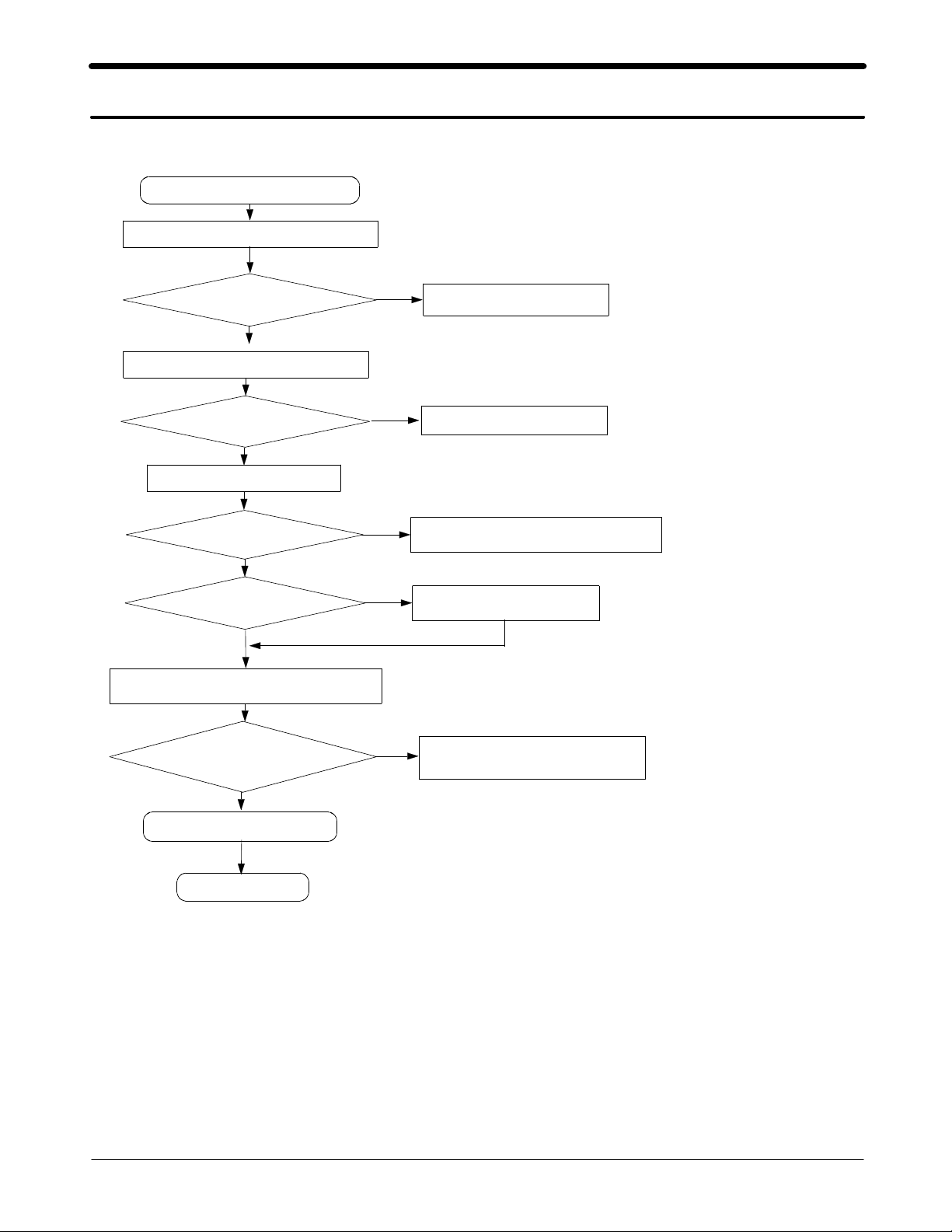
9. Flow Chart of Troubleshooting
9-1-1.
Power ON
Power On' does not work
'
Check the current consumption
Yes
Current consumption
Check the Vbat Voltage
Voltage
Check the pin of PMIC400
Pin#J12
Pin#B7
>= 100
mA
Yes
>=3.3V
Yes
:3.0V
:1.8V
Yes
No
No
No
Download again
Charge the Battery
Check PMIC400 and C413, C444, L403
Pin#A11
Check the clock signal at pin#C5 of PMIC400
Freq
Check the initial operation
in#B7
P
=1.2V
=
32.768khz
END
=1.3V
Yes
Yes
No
Check PMIC400 and L402, L404
Yes
No
Check the clock generation circuit
relatedtoOSC
(
400)
9-1
SAMSUNG Proprietary-Contents may change without notice
This Document can not be used without Samsung's authorization
Page 17
Flow Chart of Troubleshooting
1
U
0
D
4
0
1
C
4
4
5
L402
C
4
4
4
L403
6
4
4
L405
C
C447
L406
OSC802
C
C
C
C
C
C
C
C
C
C
C
4
4
4
4
4
4
1
2
1
9
3
5
C401
4
5
4
C
C
C
8
2
4
4
0
0
0
4
4
4
0
9
C
R
C406
3
5
4
C
3
4
4
C
2
1
4
L404
C811
C812
C
8
0
5
C813
C
8
0
4
C
0
0
0
4
1
8
C
C
S
O
C
C
5
4
8
8
1
1
0
1
8
8
0
5
R
R
4
0
3
2
2
7
3
1
4
0
0
4
C
I
M
P
C414
C
4
5
5
C440
C436
AP_DI
C
4
4
4
4
4
2
2
2
2
2
2
7
6
0
5
C456
C
R
R
4
4
4
0
0
0
5
6
7
3
1
4
C
9
0
4
C
9
3
4
C
1
4
4
C
0
5
4
C
8
3
4
C
4
3
4
C
2
5
0
3
4
C
4
C
3
2
4
C
C
8
4
3
4
5
4
C
8
R
3
0
1
R
3
2
U302
0
0
L
4
0
4
0
U
3
0
4
C
0
0
4
8
2
4
4
0
4
C
C
C
4
2
9
R705
D
4
0
0
0
1
4
R
9
0
4
R
R
4
0
5
C
4
3
1
7
3
4
C
0
0
1
R
0
7
6
0
7
R
Q
U
C
4
7
4
2
0
R
2
4
0
8
3
U
0
7
D
6
Z
0
5
2
0
6
R
C
6
4
0
C
3
2
2
0
D
3
0
5
L
O
V
_
M
A
C
9-2
SAMSUNG Proprietary-Contents may change without notice
This Document can not be used without Samsung's authorization
Page 18
Flow Chart of Troubleshooting
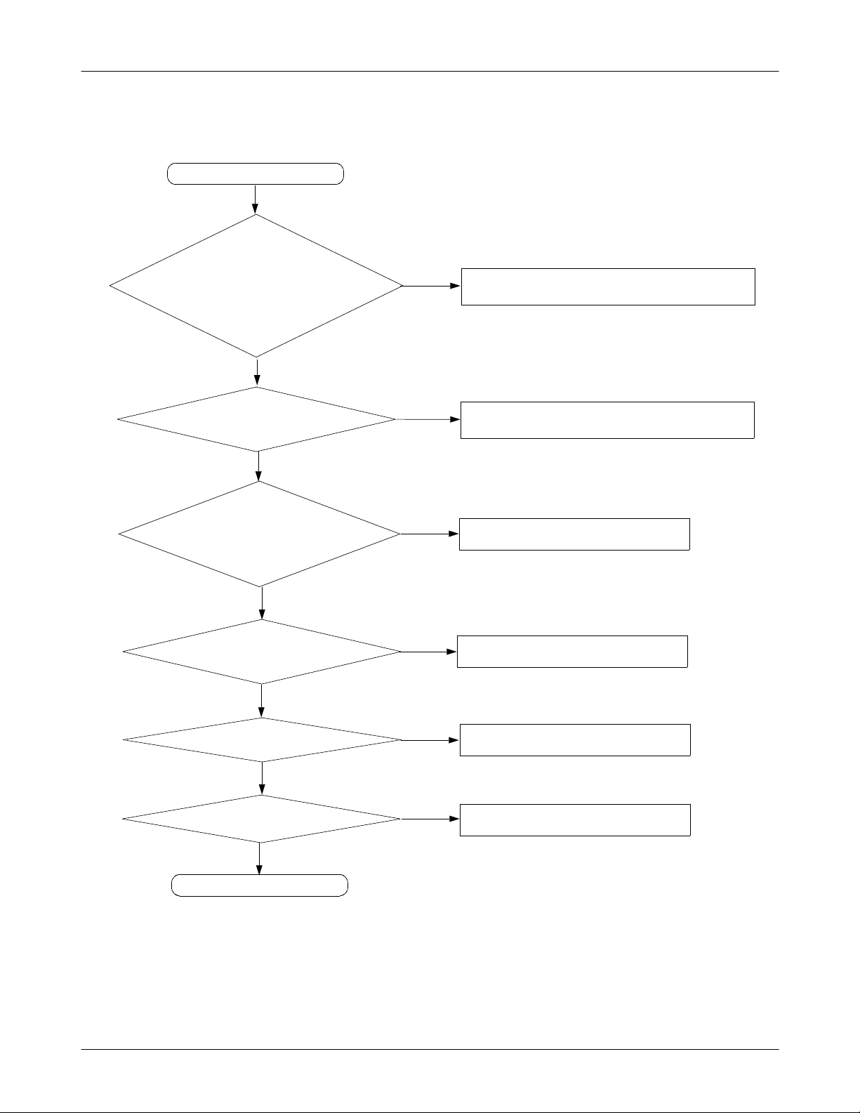
9-1-2.
Initial
Initial Failure
Yes
The pin#B6 of
and
1.
V
325
the pin#B3 of
1.8V ?
Is the pin#A14 of PMIC400
Low→High"
"
There is
forms at the
32.768
C436
PMIC400
PMIC400
Yes
?
Yes
kHz wave
and
=
C440
No
if it has some problem, it is to be replaced.)
=
No
No
(
if it has some problem, it is to be replaced.)
(
Check the PMIC400
Check the PMIC400
Check the OSC400
Yes
The voltage is"High" at the
C426, C427
C416,
C415,
Yes
LCD display is O.K
Yes
Sound is O.K
Yes
END
No
Check the PMIC400
No
Check the LCD part
No
Check the Audio part
9-3
SAMSUNG Proprietary-Contents may change without notice
This Document can not be used without Samsung's authorization
Page 19

Flow Chart of Troubleshooting
9-4
SAMSUNG Proprietary-Contents may change without notice
This Document can not be used without Samsung's authorization
Page 20

Flow Chart of Troubleshooting
9-1-3.
Sim Part
Insert SIM is displayed on the LCD
"
Yes
Check the SIM connector's
T/SIM
(
pin#9,
Is there any signals
connection to
400)
SIM card
Yes
Is there any signals
only pin#10,#11 of
#10,#11
T/SIM
of T/SIM
Yes
400 ?
400 ?
No
No
No
Resolder or change T/SIM
Check the HEA601
Check the U605
400
Yes
Check the voltage at pin#9
of T/SIM
400 >= 2.8V ?
Yes
Is there any signals
only pin#11 of T/SIM
Check the U702
END
400 ?
Yes
Yes
No
Check the PMIC201
No
Check theUCP300
9-5
SAMSUNG Proprietary-Contents may change without notice
This Document can not be used without Samsung's authorization
Page 21

Flow Chart of Troubleshooting
9
4
1
R
6
2
4
C
1
6
4
C467
C
6
6
C
4
C465
4
6
C
4
C463
T/SIM400
1
0
4
C
R
R
4
4
1
1
4
7
4
1
C
6
7
4
1
C
R
R
4
4
1
1
5
3
4
1
C
8
4
1
R
6
4
1
C
1
5
1
R
2
R513
D
5
0
Z
0
Z
D
5
0
Z
1
D
7
0
4
3
7
1
C
C712
5
4
C
3
5
3
5
C
8
U
5
0
7
8
2
5
1
R
6
4
1
R
R509
6
U
5
0
C
5
U509
C527
9-6
SAMSUNG Proprietary-Contents may change without notice
This Document can not be used without Samsung's authorization
Page 22

Flow Chart of Troubleshooting
9-1-4.
MAIN Microphone Part
Check main microphone function in voice call
receiver mode
No
Check the Voltage at
L613
=1.8V
Yes
Check component soldering
status at
R504, C508, C511 and
C512
Yes
Change the Send-end key
FPCB ass'y
Yes
END
No
Resolder or change UCP300
No
Resolder or change the components
9-7
SAMSUNG Proprietary-Contents may change without notice
This Document can not be used without Samsung's authorization
Page 23

Flow Chart of Troubleshooting
9-1-5.
Sub Microphone
Check sub microphone function in voice call loud mode
No
Check the connection status
of HEA602
Yes
Check voltage level at
C610
=2.6V
Yes
Check component soldering
R500,R501,R505,C500,C501,
status at
C502,C504,C505,L506 and
L508
Yes
No
Reconnect the HEA602
No
Resolder or change PMIC400
No
Resolder or change the components
Check the connection status
of HEA602
Yes
END
9-8
SAMSUNG Proprietary-Contents may change without notice
This Document can not be used without Samsung's authorization
Page 24

Flow Chart of Troubleshooting
9-1-6.
SPK Part
Play MP3 with maximum volume level.
Check speaker function.
No
Check the signal output of
TP400,TP401,TP403..
Yes
Check the signal output of
C286 and C287.
Yes
Check the signal signal
output of C602 and C603.
Yes
Check the connection of
HEA601
No
No
No
Resolder or change UCP701
Check component soldering
U400,C404,C408,C409,C418,
Resolder or change the components.
Reconnect HEA601
status at
C421,C422
NO
Yes
Replace the speaker module.
Yes
End
9-9
SAMSUNG Proprietary-Contents may change without notice
This Document can not be used without Samsung's authorization
Page 25

Flow Chart of Troubleshooting
9-1-7.
Receiver Part
Check receiver function in
voice call receiver mode
Check the signal of V400
and V401.
Is the signal phase reversed?
Check the signal of pin
and#7at U403.
Is the signal phase reversed
and DC bias
Check the signal output of
C267 and C279?
Yes
Yes
=1.2
Yes
Yes
V?
No
Resolder or change U403
#5
No
Resolder or change U400
No
Resolder or change UCP300
Replace the Earjack-SubMic-
Receiver ass'y
Yes
End
9-10
SAMSUNG Proprietary-Contents may change without notice
This Document can not be used without Samsung's authorization
Page 26

Flow Chart of Troubleshooting
RF
9-2.
9-2-1.
GSM
850
RX
NORMAL CONDITION
catch the channel?
pin
Check the Voltage at
C111
NO
U104 CHECK
dBm
2≤-65
=2.8V?
YES
?
YES
NO
No
CHECK soldered
RFS100, C102, L100
U205, C111, C117
resolder or change
CONTINUOUS RX ON
RF INPUT
AMP
:-50
: 190
dBm
CH
U104 CHECK
pin
12,13≥-65
Check component
soldering status at L129,
L130, L104
C112
{
C148
&{
pin2of U100
freq
YES
U100
=2.1V?}
=2.7V?}
YES
CHECK
MHz
:19.2
YES
dBm
YES
?
?
NO
NO
resolder or change
NO
resolder or change
NO
OSC
change or resolder
U104
L129, L130, L104
PMIC400
resolder or change
100
U100
pin
13,14
: 120mV?
YES
GSM850 Receiver is O.K?
YES
END
NO
NO UCP300
U100
resolder or change
resolder or change
9-11
SAMSUNG Proprietary-Contents may change without notice
This Document can not be used without Samsung's authorization
Page 27

Flow Chart of Troubleshooting
9-2-2.
GSM
900
RX
NORMAL CONDITION
catch the channel?
NO
U104 CHECK
pin
Check the Voltage at
C111
U104 CHECK
pin
14,15≥-65
Check component
soldering status at L105,
dBm
2≤-65
=2.8V?
L106, L107
YES
dBm
YES
?
YES
No
NO
NO
?
NO
CHECK soldered
RFS100, C102, L100
U205, C111, C117
resolder or change
U104
resolder or change
L105, L106, L107
resolder or change
CONTINUOUS RX ON
RF INPUT
AMP
:-50
:37
dBm
CH
YES
U100
C112
{
=2.1V?}
C148
&{
GSM900 Receiver is O.K?
=2.7V?}
U100 CHECK
pin
2
freq
MHz
:19.2
U100
pin
13,14
: 120mV?
YES
YES
END
YES
?
YES
NO
resolder or change
NO
NO
NO UCP300
OSC
change or resolder
100
U100
resolder or change
resolder or change
PMIC400
9-12
SAMSUNG Proprietary-Contents may change without notice
This Document can not be used without Samsung's authorization
Page 28

Flow Chart of Troubleshooting
9-2-3.
DCS RX
NORMAL CONDITION
catch the channel?
NO
U104 CHECK
pin
Check the Voltage at
C111
U104 CHECK
pin
16,17≥-65
Check component
soldering status at L127,
dBm
2≤-65
=2.8V?
L128, L108
YES
dBm
YES
?
YES
?
NO
NO
NO
No
CHECK soldered
RFS100, C102, L100
U205, C111, C117
resolder or change
U104
resolder or change
L127, L128, L108
resolder or change
CONTINUOUS RX ON
RF INPUT
AMP
:-50
: 698
dBm
CH
YES
U100
C112
{
=2.1V?}
C148
&{
DCS Receiver is O.K?
CHECK
U100 pin
freq
:19.2
pin
: 120mV?
=2.7V?}
YES
2
MHz
YES
U100
15,16
YES
YES
END
?
NO
resolder or change
NO
NO
NO UCP300
OSC
change or resolder
100
U100
resolder or change
resolder or change
PMIC400
9-13
SAMSUNG Proprietary-Contents may change without notice
This Document can not be used without Samsung's authorization
Page 29

Flow Chart of Troubleshooting
9-2-4.
PCS RX
NORMAL CONDITION
catch the channel?
NO
U104 CHECK
pin
Check the Voltage at
C111
U104 CHECK
pin
16,17≥-65
Check component
soldering status at L127,
dBm
2≤-65
=2.8V?
L128, L108
YES
dBm
YES
?
YES
?
NO
NO
NO
No
CHECK soldered
RFS100, C102, L100
U205, C111, C117
resolder or change
U104
resolder or change
L127, L128, L108
resolder or change
CONTINUOUS RX ON
RF INPUT
AMP
:-50
: 661
dBm
CH
YES
U100
C112
{
=2.1V?}
C148
&{
PCS Receiver is O.K?
=2.7V?}
U100 CHECK
pin
2
freq
MHz
:19.2
U100
pin
15,16
: 120mV?
YES
YES
END
YES
?
YES
NO
NO
change or resolder
NO
NO
PMIC400
resolder or change
OSC
100
U100
resolder or change
UCP300
resolder or change
9-14
SAMSUNG Proprietary-Contents may change without notice
This Document can not be used without Samsung's authorization
Page 30

Flow Chart of Troubleshooting
9-2-5.
WCDMA Band1 Rx
NORMAL CONDITION
catch the channel?
U104 CHECK
pin
2≤-65
Check the Voltage at
C111
=2.8V?
U104 CHECK
pin
22≥-65
U100 CHECK
pin
36≥-65
dBm
YES
dBm
YES
dBm
NO
?
YES
No
NO
NO
?
NO
?
CHECK soldered
RFS100, C102, L100
U205, C111, C117
resolder or change
U104
resolder or change
C166, C169, DUF100,
R107, L116, C172
resolder or change
CONTINUOUS RX ON
RF INPUT
AMP
:-50
: 661
dBm
CH
YES
U100
C112
{
=2.1V?}
C148
&{
W2100 Receiver is O.K?
=2.7V?}
U100 CHECK
pin
2
freq
MHz
:19.2
U100
pin
29,30
: 120mV?
YES
YES
END
YES
?
YES
NO
NO
change or resolder
NO
NO
resolder or change
OSC
100
U100
resolder or change
resolder or change
9-15
PMIC400
UCP300
SAMSUNG Proprietary-Contents may change without notice
This Document can not be used without Samsung's authorization
Page 31

Flow Chart of Troubleshooting
9-2-6.
WCDMA Band5 Rx
NORMAL CONDITION
catch the channel?
U104 CHECK
pin
2≤-65
Check the Voltage at
C111
=2.8V?
U104 CHECK
pin
21≥-65
U100 CHECK
pin
30,31≥-65
dBm
YES
dBm
YES
NO
YES
dBm
No
?
NO
NO
?
NO
?
CHECK soldered
RFS100, C102, L100
U205, C111, C117
resolder or change
U104
resolder or change
C184, DUF101,C188,
C191, L122
resolder or change
CONTINUOUS RX ON
RF INPUT
AMP
:-50
: 661
dBm
CH
YES
U100
C112
{
=2.1V?}
C148
&{
W850 Receiver is O.K?
=2.7V?}
YES
RFT100 CHECK
pin
2
freq
MHz
:19.2
YES
RFT100
pin
15,16
: 120mV?
YES
YES
END
?
NO
NO
change or resolder
NO
NO
resolder or change
OSC
100
RFT100
resolder or change
9-16
PMIC400
UCP300
resolder or change
SAMSUNG Proprietary-Contents may change without notice
This Document can not be used without Samsung's authorization
Page 32

Flow Chart of Troubleshooting
9-2-7.
GSM
850
U104 pin
about
2~3
RFS
L100,C102
100,
check&change
NO
dBm?
YES
2:
TX
about
pin
about
L117
:30
U105
4 : 3.8V ?
U105 pin
:-5
NO
YES
dBm
dBm
CONTINOUS TX ON CONDITION
TX POWER DAC:
NO
8
?
C111
YES
NO
YES
V?
:2.8
YES
U104
change or resolder
Check
DC bias
U105
change or resolder
NO
U205
check&change
REF LEV.
RBW
VBW
SPAN
ATT.
CH
600
:62
: 100
:100
:10
:20
CODE APPLIED
KHz
KHz
MHz
dBm
:10
dB
NO
U100 pin
about
C112
{
&{
C148
:-5
NO
U100
=2.1V?}
=2.7V?}
dBm
55
YES
NO
YES
U100 CHECK
pin
2
freq
:19.2
MHz
?
YES
U100
pin
63,64
: 120mV?
YES
GSM850 Tranceiver is O.K?
C115, R113, R109,
R114
change or resolder
PMIC400
resolder or change
NO
NO
NO
OSC
change or resolder
100
U100
resolder or change
resolder or change
UCP300
YES
END
9-17
SAMSUNG Proprietary-Contents may change without notice
This Document can not be used without Samsung's authorization
Page 33

Flow Chart of Troubleshooting
9-2-8.
GSM
900
U104 pin
about
2~3
RFS
L100,C102
100,
check&change
NO
dBm?
YES
TX
2:
about
pin
U105 pin
about
L117
dBm
:30
NO
U104
4 : 3.8V ?
YES
dBm
:-5
NO
8
?
C111
YES
NO
YES
V?
:2.8
YES
U104
change or resolder
Check
DC bias
U104
change or resolder
NO
U205
check&change
NO
U100 pin
55
about
dBm
:-5
NO
&{
C112
{
C148
U100
=2.1V?}
NO
=2.7V?}
YES
U100 CHECK
pin
2
freq
:19.2
MHz
?
YES
U100
pin
65,66
: 120mV?
YES
GSM Receiver is O.K?
C115, R113, R109,
YES
change or resolder
PMIC400
resolder or change
NO
R114
change or resolder
NO
NO
OSC
100
U100
resolder or change
UCP300
resolder or change
YES
END
9-18
SAMSUNG Proprietary-Contents may change without notice
This Document can not be used without Samsung's authorization
Page 34

Flow Chart of Troubleshooting
9-2-9.
DCS TX
U104 pin
about
2~3
RFS
100,
check&change
NO
2:
dBm?
YES
L100,C102
about
about
pin
4 : 3.8V ?
U105 pin
L118
:30
U105
:-5
NO
YES
dBm
dBm
NO
1
?
C111
YES
NO
YES
V?
:2.8
YES
U104
change or resolder
Check
DC bias
U105
change or resolder
NO
U205
check&change
NO
U100 pin
56
about
dBm
:-5
NO
&{
C112
{
C148
U100
=2.1V?}
NO
=2.7V?}
YES
U100 CHECK
pin
2
freq
:19.2
MHz
?
YES
U100
pin
63,64
: 120mV?
YES
DCS Receiver is O.K?
C110, R113, R109,
YES
change or resolder
PMIC400
resolder or change
NO
R114
change or resolder
NO
NO
OSC
100
U100
resolder or change
UCP300
resolder or change
YES
END
9-19
SAMSUNG Proprietary-Contents may change without notice
This Document can not be used without Samsung's authorization
Page 35

Flow Chart of Troubleshooting
9-2-10.
PCS TX
U104 pin
about
2~3
RFS
L100,C102
100,
check&change
NO
dBm?
YES
2:
about
pin
U105 pin
about
L118
dBm
:30
NO
U105
4 : 3.8V ?
YES
dBm
:-5
NO
1
?
C111
YES
NO
YES
V?
:2.8
YES
U104
change or resolder
Check
DC bias
U105
change or resolder
NO
U205
check&change
NO
U100 pin
56
about
dBm
:-5
NO
&{
C112
{
C148
U100
=2.1V?}
NO
=2.7V?}
YES
U100 CHECK
pin
2
freq
:19.2
MHz
?
YES
U100
pin
63,64
: 120mV?
YES
PCS Receiver is O.K?
C110, R110, R111,
YES
change or resolder
PMIC400
resolder or change
NO
R112
change or resolder
NO
NO
OSC
100
U100
resolder or change
UCP300
resolder or change
YES
END
9-20
SAMSUNG Proprietary-Contents may change without notice
This Document can not be used without Samsung's authorization
Page 36

Flow Chart of Troubleshooting
9-2-11.
WCDMA Band1 TX
C166
:20
C171
:20
L115
:-5
NO
dBm
NO
dBm
dBm
U104 pin
about
2~3
RFS
L100,C102
100,
check&change
dBm?
YES
2:
about
about
about
C111
YES
change or resolder
C171, C174, DUF100,
YES
change or resolder
YES
change or resolder
V?
:2.8
YES
U104
C166, C169
PAM100
NO
U205
check&change
NO
dBm
NO
=2.7V?}
YES
NO
&{
about
C112
{
C148
C108
:-5
U100
=2.1V?}
YES
U100 CHECK
pin
2
freq
:19.2
MHz
?
YES
U100
pin
63,64
: 120mV?
YES
W2100 Transmitter is O.K?
C108, L114, F101,
C165, L115
resolder or change
PMIC400
resolder or change
NO
NO
OSC
change or resolder
resolder or change
NO
100
U100
UCP300
resolder or change
YES
END
9-21
SAMSUNG Proprietary-Contents may change without notice
This Document can not be used without Samsung's authorization
Page 37

Flow Chart of Troubleshooting
9-2-11.
WCDMA Band5 TX
C184
:20
L121
:20
L115
:-5
NO
dBm
NO
dBm
dBm
U104 pin
about
2~3
RFS
L100,C102
100,
check&change
dBm?
YES
2:
about
about
about
C111
YES
YES
YES
V?
:2.8
YES
U104
change or resolder
L121, C190, CPL100,
DUF101, C184
change or resolder
PAM102
change or resolder
NO
U205
check&change
NO
dBm
NO
=2.7V?}
YES
NO
&{
about
C112
{
C148
C109
:-5
U100
=2.1V?}
YES
U100 CHECK
pin
2
freq
:19.2
MHz
?
YES
U100
pin
63,64
: 120mV?
YES
W850 Transmitter is O.K?
C109, L124, C194,
F102, C125, C193
resolder or change
PMIC400
resolder or change
NO
NO
NO
OSC
change or resolder
100
U100
resolder or change
resolder or change
UCP300
YES
END
9-22
SAMSUNG Proprietary-Contents may change without notice
This Document can not be used without Samsung's authorization
Page 38

Flow Chart of Troubleshooting
9-3.
Bluetooth
Check BT function
ON
Yes
Check the Voltage at
C218
=3.0V
Yes
Check26MHz clock at
C202 point
Yes
Check the Voltage of
L207
=1.5V
Yes
Check the status
at C204
No
Enable BT function
No
Check PMIC400
No
Check OSC200
No
Resolder or change L207
No
Resolder or Replace C204
END
Yes
9-23
SAMSUNG Proprietary-Contents may change without notice
This Document can not be used without Samsung's authorization
Page 39

Flow Chart of Troubleshooting
1
C458
8
S
O
1
R
0
A
1
C109
R114
R
1
5
1
C169
0
P
0
1
A
T
R
1
1
6
C123
1
0
C
1
R
1
9
1
0
M
C208
R204
L
2
0
1
6
0
R
2
R
2
7
0
R
2
8
0
R
2
9
0
R
2
5
0
1
1
R
2
R
2
0
1
C
2
0
7
C
2
1
3
C
5
2
1
C205
0
3
U
C
C
2
2
0
1
9
0
U
2
0
4
U300
C302
3
0
C
1
2
1
2
C
C
2
1
8
9-24
SAMSUNG Proprietary-Contents may change without notice
This Document can not be used without Samsung's authorization
Page 40

Flow Chart of Troubleshooting
9-4.
FM Radio Part
FM Radio does not work
Yes
Check the connection
at HEA400
Yes
Check the Audio signal
at C416, C417 and
C525
No
Yes
connect earjack to HEA400
Check the Audio signal
at C260, C262
Yes
Check the Audio signal
at L400, L401
C602, C603; SPK)
(
No
No
Check U400
Resolder L400, L401 and
check PMIC400
No
Check the
supply at C216
Check the FM RF
signal at C207
change the main PBA
3.0V
Yes
Yes
No
No
Yes
change earjack ASSY
Check U200
change earjack ASSY
9-25
SAMSUNG Proprietary-Contents may change without notice
This Document can not be used without Samsung's authorization
Page 41

Flow Chart of Troubleshooting
9-26
SAMSUNG Proprietary-Contents may change without notice
This Document can not be used without Samsung's authorization
Page 42

Block Diagrams
7.
Main Block Diagram
7-1.
7-1
SAMSUNG Proprietary-Contents may change without notice
This Document can not be used without Samsung's authorization
Page 43

RF Solution Block Diagram
7-2.
Block Diagrams
7-2
SAMSUNG Proprietary-Contents may change without notice
This Document can not be used without Samsung's authorization
Page 44

PCB Diagrams
8.
8-1.
Main Top
□
8-1
SAMSUNG Proprietary-Contents may change without notice
This Document can not be used without Samsung's authorization
Page 45

PCB Diagrams
8-2.
Main Bottom
8-2
SAMSUNG Proprietary-Contents may change without notice
This Document can not be used without Samsung's authorization
Page 46

11
7-1.
1.
make gap between Screw cover and Rear.
2.
easily.
Disassembly and Assembly Instructions
.
Disassembly
1 2
Remove the screw cover
Useadecomposition tool to Screw cover part and
Usingadecomposition tool, locker is disintegrated
Remove screw
Remove6Screws.
1.
3
Separate the PBA from FRONT Ass'y.
Separate the Rear
Separate lower part corner usingadecomposition tool.
1.
4
Separate all corners usingadecomposition tool.
1.
Lift the rear from the front with care.
2.
Separate the Rear
11-1
SAMSUNG Proprietary-Contents may change without notice
This Document can not be used without Samsung's authorization
Page 47

Exploded View and Parts List
5
Separate the Hold key dome sheet
Separate hold key form bracket with care.
1.
7
6
Separate the Volume&Cam key dome sheet
Separate the Volume&Cam Key dome sheet from
1.
bracket with care.
8
Separate the PBA from FRONT Ass'y.
Separate the PBA from the FRONT Ass'y.
1.
Separate the OLED connector from PBA.
Separate the OLED connector from PBA
1.
11-2
SAMSUNG Proprietary-Contents may change without notice
This Document can not be used without Samsung's authorization
Page 48

Exploded View and Parts List
9
Separate the bracket.
Separate the lower part right corner using
1.
decomposition tool.
Separate all corners usingadecomposition tool.
2.
11
Separate the TSP&Sub key FPCB
10
Separate the sub key pad
a
Get each flange of the sub key pad out.
1.
Push the flange to separate using the tweezers
2.
12
Separate the OLED from the Front
Unlock the connector of the TSP&sub key FPCB
1.
Separate the TSP&sub key FPCB.
2.
SAMSUNG Proprietary-Contents may change without notice
This Document can not be used without Samsung's authorization
Separate OLED from the front with great care.(Be
1.
careful not to crack TSP&OLED.)
11-3
Page 49

Exploded View and Parts List
13
Separate the TP from the Front
Separate the TSP from the front with great care.(Be
1.
careful not to crack TSP.)
15
Separate the RCV, Motor, Mic Ass'y
14
Separate the
1.
Separate the
12M
Cam Ass'y from the PBA
12M
Cam, CIF Cam, Zenon flash
connector.(Be careful not to crack chip.)
Push the bottom of the
2.
Cam to separate the
12M
module.
16
Separate the CIF Cam, Light sensor Ass'y
Separate the RCV, Mic, Motor in the order named.
1.
Separate the connector from
2.
Be careful not to damage the RCV, Mic, Motor FPCB.)
(
12M
Cam Ass'y.
SAMSUNG Proprietary-Contents may change without notice
This Document can not be used without Samsung's authorization
Separate the CIF Cam, light sensor in the order
1.
named.
Separate the connector PCB.
2.
Be careful not to damage the CIF Cam, ligtht sensor,
(
FPCB)
11-4
Page 50

Exploded View and Parts List
17
Separate the Auto Lens Cap
Remove4Screws.
1.
19
18
Separate SPK&Intenna module like the picture.
1.
Be careful not to damage rear and SPK&Intenna
(
Separate the SPK&Intenna module.
module.)
11-5
SAMSUNG Proprietary-Contents may change without notice
This Document can not be used without Samsung's authorization
Page 51

Exploded View and Parts List
Assembly
7-2
1
Assemble VGA module
1) Get rid of the tape.
2) Insert the connector into the poles of the module.
2
Assemble VGA module
1) Put the light sensor into the rib first.
2) Put the VGA camera into the module.
3 4
1)
PBA.
2)
※
1) Be care of an electric shock. Do not touch the 330V
capacitor.
Assemble RCV module
Combine the connector of the motor with the sub
Put the receiver into the module.
Caution
Assemble RCV module
1) Hook the PFCB on the rib and put the MIC on the
module.
Caution
※
1) Be care of an electric shock. Do not touch the 330V
capacitor.
11-6
SAMSUNG Proprietary-Contents may change without notice
This Document can not be used without Samsung's authorization
Page 52

Exploded View and Parts List
5
Assemble12Mega Zenon module
1) Insert the poles of the module into the holes of the
PBA
2) Check the state of the assembled module
Caution
※
1) Do not touch the FPCB when assemble the module
2) Be care of an electric shock. Do not touch the 330V
capacitor.
7
Assemble TSP
6
Assemble12Mega Zenon module
1) Connect the module connectors with the PBA.
Caution
※
1) Be care of an electric shock. Do not touch the 330V
capacitor.
8
Assemble TSP
1) Insert the FPCB of the TSP into the hole of the front
2) Put the TSP on the upper of the front first
SAMSUNG Proprietary-Contents may change without notice
This Document can not be used without Samsung's authorization
1) Put the TSP on the lower of the front next.
11-7
Page 53

Exploded View and Parts List
9
Assemble Sub Key Pad
1) Put the key pad on the front.
2) Hook the holes of the pad on the poles of the front
by a pincette
11
Assemble PBA
10
Assemble OLED LCD
1) Put the LED on the front matching the point.
Insert the FPCBs into the connectors matching the
2)
silk line.
12
Assemble Side Key FPCB
1) Put the LED FPCB though the hole of the bracket
Caution
※
1) Hold and pull the FPCB not to be damaged
SAMSUNG Proprietary-Contents may change without notice
This Document can not be used without Samsung's authorization
1)InsertthePOGOpinintotheholeontherear
11-8
Page 54

Exploded View and Parts List
13
Assemble Auto Lens cap
Screw the auto cap on the rear.(4POINT)
1)
14
Ass'y PBA
Connect the front ass'y and PBA ass'y.
1)
Caution
※
1) Be care of an electric shock. Do not touch the 330V
capacitor.
15
Assemble PBA
1) Put the PBA ass'y on the front
16
Assemble Side Key FPCB
1) Get rid of the tapes behind key FPCBs.
2) Attach the FPCBs on the side of the bracket.
11-9
SAMSUNG Proprietary-Contents may change without notice
This Document can not be used without Samsung's authorization
Page 55

Exploded View and Parts List
17
1)
19
Assemble Rear
Assemble the rear into the front ass'y left side first.
Check the assembled state
18
1)
Assemble Rear
Press the right side of the rear next and the other
sides.
20
Assemble screw
1) Check the assembled state of the set not to make a
gap
SAMSUNG Proprietary-Contents may change without notice
This Document can not be used without Samsung's authorization
1) Screw the 6 points into the rear.
11-10
Page 56

Exploded View and Parts List
21
Assemble Rear cover
Insert the hook into the hole of the rear first.
1)
Press the cover to assemble.
2)
22
Check the Set
Check all the state of the set.
1)
11-11
SAMSUNG Proprietary-Contents may change without notice
This Document can not be used without Samsung's authorization
Page 57

efrcom
 Loading...