

Approval
TO
DATE
SAMSUNG TFT-LCD
SAMSUNG TFT-LCD
MODEL NO. : LTN184KT01-A01
MODEL NO. : LTN184KT01-A01
NOTE : Extension code [ -A01 ]
www.jxlcd.com
: Acer/Inventec
: Apr. 29, 2008
www.jxlcd.com
Surface type [ Glare ]
→ LTN184KT01-A01
Any modification is not allowed without SEC’s permission
APPROVED BY :
PREPARED BY :
LCD DEVELOPMENT G1. MOBILE DIVISION
SAMSUNG ELECTRONICS CO., LTD.
Samsung Secret
Doc.No. Rev.No
Kevin Kim
04-A00-G-080429
Page
/ 31LTN184KT01-A01
1
CONTENTS
Approval
Revision History
General Description
1. Absolute Maximum Ratings
1.1 Absolute Ratings of environment
1.2 Electrical Absolute Ratings
2. Optical Characteristics
3. Electrical Characteristics
3.1 TFT LCD Module
3.2 Backlight Unit
3.3 Inverter
4. Block Diagram
4.1 TFT LCD Module
4.2 Backlight Unit
4.3 Inverter Unit
5. Input Terminal Pin Assignment
5.1 Input Signal & Power
5.2 LVDS Interface
5.3 Backlight Unit
www.jxlcd.com
www.jxlcd.com
5.4 Timing Diagrams of LVDS For Transmitting
5.5 Input Signals, Basic Display Colors and Gray Scale of Each Color.
5.6 Pixel format
5.7 Inverter Signals & Power
- - - - - - - - - - - - - - - - - - - ( 3 )
- - - - - - - - - - - - - - - - - - - ( 4 )
- - - - - - - - - - - - - - - - - - - ( 5 )
- - - - - - - - - - - - - - - - - - - ( 7 )
- - - - - - - - - - - - - - - - - - - ( 10 )
- - - - - - - - - - - - - - - - - - - ( 13 )
- - - - - - - - - - - - - - - - - - - ( 14 )
6. Interface Timing
6.1 Timing Parameters
6.2 Timing Diagrams of interface Signal
6.3 Power ON/OFF Sequence
7. Outline Dimension
8. Packing
9. Marking & Others
10. General Precaution
11. EDID
Samsung Secret
Doc.No. Rev.No
-- - - - - - - - - - - - - - - - - - ( 20 )
-- - - - - - - - - - - - - - - - - - - ( 22 )
-- - - - - - - - - - - - - - - ---- -- ( 24 )
--- - - - - - - - - - - - - - - - -- - ( 25 )
--- - - - - - - - - - - - - - - - - - ( 27 )
--- - - - - - - - - - - - - - - - - - ( 29 )
04-A00-G-080429
Page
/ 31LTN184KT01-A01
2
REVISION HISTORY
REVISION HISTORY
LTN184KT01-A01 model Preliminary spec was issued first.AllA00Apr. 29. 2008
Approval
SummaryPageRevision No.Date
www.jxlcd.com
www.jxlcd.com
Samsung Secret
Doc.No. Rev.No
04-A00-G-080429
Page
/ 31LTN184KT01-A01
3
Approval
GENERAL DESCRIPTION
DESCRIPTION
LTN184KT01-A01 is a color active matrix TFT (Thin Film Transistor) liquid crystal display
(LCD) that uses amorphous silicon TFT as switching devices. This model is composed
of a TFT LCD panel, a driver circuit and a backlight unit. The resolution of a 18.4" contains
1680X945 pixels and can display up to 262,144 colors. 6 O'clock direction is the
optimum viewing angle.
FEATURES
• High contrast ratio, high aperture structure
• 1680 X 945 pixels resolution (16:9)
• High Color Gamut (Typical 60%)
• Low power consumption
• Fast Response
• Single CCFL
• DE(Data enable) only mode
• 3.3V LVDS Interface
• Onboard EEDID chip
• RoHS Compliance
• Windows Vista Premium Logo compliance
APPLICATIONS
• Notebook PC
• If the usage of this product is not for PC application, but for others, please contact SEC
www.jxlcd.com
GENERAL INFORMATION
Display area
Driver element
Display colors
Number of pixel
Pixel arrangement
Pixel pitch
Display Mode
www.jxlcd.com
mm408.24(H) x 229.635(V) ( 18.4” diagonal )
a-Si TFT active matrix
262,144
RGB vertical stripe
mm0.243(H) x 0.243(V) (TYP.)
Normally white
NoteUnitSpecificationItem
16 : 9pixel1680 X 945
Glass Thickness
Surface treatment
Samsung Secret
Doc.No. Rev.No
Haze 0, Hardness 3H
04-A00-G-080429
mm0.5
Page
/ 31LTN184KT01-A01
4
Mechanical Information
Approval
Module
size
Note (1) Measurement condition of outline dimension
. Equipment : Vernier Calipers
. Push Force : 500g ⋅f (minimum)
1. ABSOLUTE MAXIMUM RATINGS
1.1 ENVIRONMENTAL ABSOLUTE RATINGS
Operating temperate
(Temperature of glass surface)
Max.
423.0
246.5
6.5
750
NoteUnitTyp.Min.Item
mm422.5422.0Horizontal (H)
mm246.0245.5Vertical (V)
(1)mm6.2-Depth (D)
g725-Weight
NoteUnitMax.Min.SymbolItem
(1),(5)°C60-20 TSTGStorage temperate
(1),(5)°C500TOPR
(2),(4)G240-SnopShock ( non-operating )
Note (1) Temperature and relative humidity range are shown in the figure below.
95 % RH Max. (40 °C ≥ Ta)
Maximum wet - bulb temperature at 39 OC or less. (Ta > 40 °C ) No condensation
www.jxlcd.com
www.jxlcd.com
100
-40 -20 0 20 40 60 80
Relative Humidity ( %RH)
90
80
60
40
20
Operating Range
Storage Range
5
0
( 40,90 )
( 50,50.4 )
( 60,27.7 )
Temperature (OC)
(2) 2ms, half sine wave, one time for ±X, ±Y, ± Z.
(3) 5 - 500 Hz, random vibration, 30min for X, Y, Z.
(4) At testing Vibration and Shock, the fixture in holding the Module to be tested have to be
hard and rigid enough so that the Module would not be twisted or bent by the fixture.
(5) If product is used for extended time excessively or exposed to high temperatures for extended time,
there is a possibility of wide viewing angle film damage which could affect visual characteristics.
(3),(4)G2.41-VnopVibration (non-operating)
Samsung Secret
Doc.No. Rev.No
04-A00-G-080429
Page
/ 31LTN184KT01-A01
5
1.2 ELECTRICAL ABSOLUTE RATINGS
Approval
(1) TFT LCD MODULE
Power Supply Voltage
Logic Input Voltage
Note (1) Within Ta (25 ± 2 °C )
(2) BACK-LIGHT UNIT
Lamp Current
Lamp frequency
Note 1) Permanent damage to the device may occur if maximum values are exceeded
Functional operation should be restricted to the conditions described under normal operating conditions.
L
L
DD
IN
DD
DD
VDD=3.3V, V
+ 0.3VDD- 0.3V
+ 0.3VDD- 0.3V
SS
= GND = 0V
NoteUnitMax.Min.SymbolItem
(1)VV
(1)VV
Ta = 25 ± 2 °C
NoteUnitMax.Min.SymbolItem
(1)mArms7.02.0I
(1)kHz8040F
www.jxlcd.com
www.jxlcd.com
Samsung Secret
Doc.No. Rev.No
04-A00-G-080429
Page
/ 31LTN184KT01-A01
6
Approval
2. OPTICAL CHARACTERISTICS
The following items are measured under stable conditions. The optical characteristics
should be measured in a dark room or equivalent state with the methods shown in Note (5).
Measuring equipment : TOPCON BM-5A and PR-650
Contrast Ratio
(5 Points)
Response Time at Ta
( Rising + Falling )
Average Luminance
of White (5 Points)
Red
Color
Chromaticity
( CIE )
Green
Blue
www.jxlcd.com
www.jxlcd.com
CR
RT
* Ta = 25 ± 2 °C, VDD=3.3V, fv= 60Hz, f
AVE
Normal
X
Y
X
Y
X
Y
Viewing
Angle
φ = 0
θ = 0
DCLK
= 53.82MHz, IL= 6.5 mA
Unit
-
msec
2
-220190YL,
0.6860.6560.626R
0.3570.3270.297R
0.2500.2200.190G
0.7050.6750.645G
0.1760.1460.116B
0.1050.0750.045B
cd/m
-
NoteMaxTyp.Min.ConditionSymbolItem
(1), (2), (5)-800500
(1), (3)168-T
IL=6.5mA
(1), (4)
(1), (5)
PR-650
White
Viewing
Angle
13 Points/5 Points
White Variation
Hor.
Ver.
Hor.
Ver.
X
Y
θ
L
H
H
L
θ
L
θ
H
φ
H
φ
L
L
CR ≥ 10
CR ≥ 100
-
-
-
-
0.3430.3130.283W
0.3590.3290.299W
-4540
-4540θ
-3015φ
-1535φ
-
---
-
---
Degrees
(1), (5)
BM-5A
(6)-1.7/1.25--δ
Samsung Secret
Doc.No. Rev.No
04-A00-G-080429
Page
/ 31LTN184KT01-A01
7
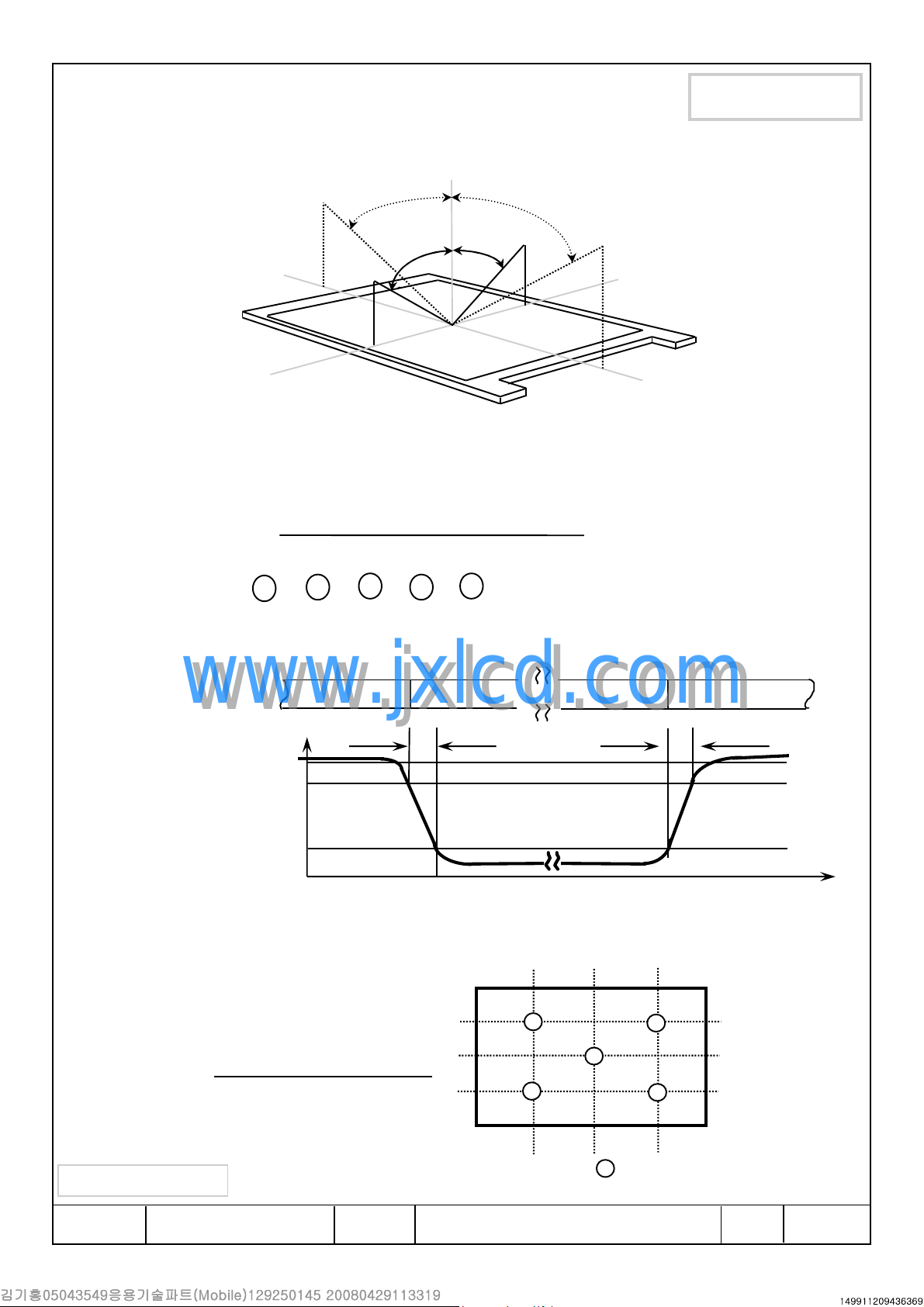
Note 1) Definition of Viewing Angle : Viewing angle range(10
Normal Line
o
φ = 0
,
θ = 0
θ
L
φ
H
θL =90
φ
o
x
L
≤≤≤≤
o
C/R)
θ
R
Approval
12 O’clock
y
direction
φH= 90
o
6 O’clock
direction
φL= 90
Note 2) Definition of Contrast Ratio (CR) : Ratio of gray max (Gmax) ,gray min (Gmin)
at 5 points(4, 5, 7, 9, 10)
Points : , , , , at the figure of Note (6).
Note 3) Definition of Response time :
Display data
Optical
Response
o
CR(4) + CR(5) + CR(7) + CR(9) + CR(10)
CR =
4 9
www.jxlcd.com
www.jxlcd.com
100%
90%
10%
0%
5
White(TFT OFF) White(TFT OFF)
7
5
10
Black(TFT ON)
T
R
x'y'
θR=90
T
F
o
Note 4) Definition of Average Luminance of White : measure the luminance of white at 5 points.
(420) ( 840) (1260)
Average Luminance of White ( Y
YL4+ YL5+ YL7+ YL9+ Y
Y
L,AVE
=
Samsung Secret
Doc.No. Rev.No
5
L,AVE
)
L10
10
9
7
5
4
: test point
04-A00-G-080429
Time
VIEW AREA
(236)
(473)
(709)
(lines)
Page
/ 31LTN184KT01-A01
8
Approval
Note 5) After stabilizing and leaving the panel alone at a given temperature for 30 min , the measurement
should be executed. Measurement should be executed in a stable, windless,and dark room.
30 min after lighting the backlight. This should be measured in the center of screen.
Lamp current : 6.5mA ( Inverter : SIC-130T )
Environment condition : Ta = 25 ± 2 °C
Photo-detector
( TOPCON SR3 )
Field
= 2°
50 cm
TFT-LCD module
Center of the screen
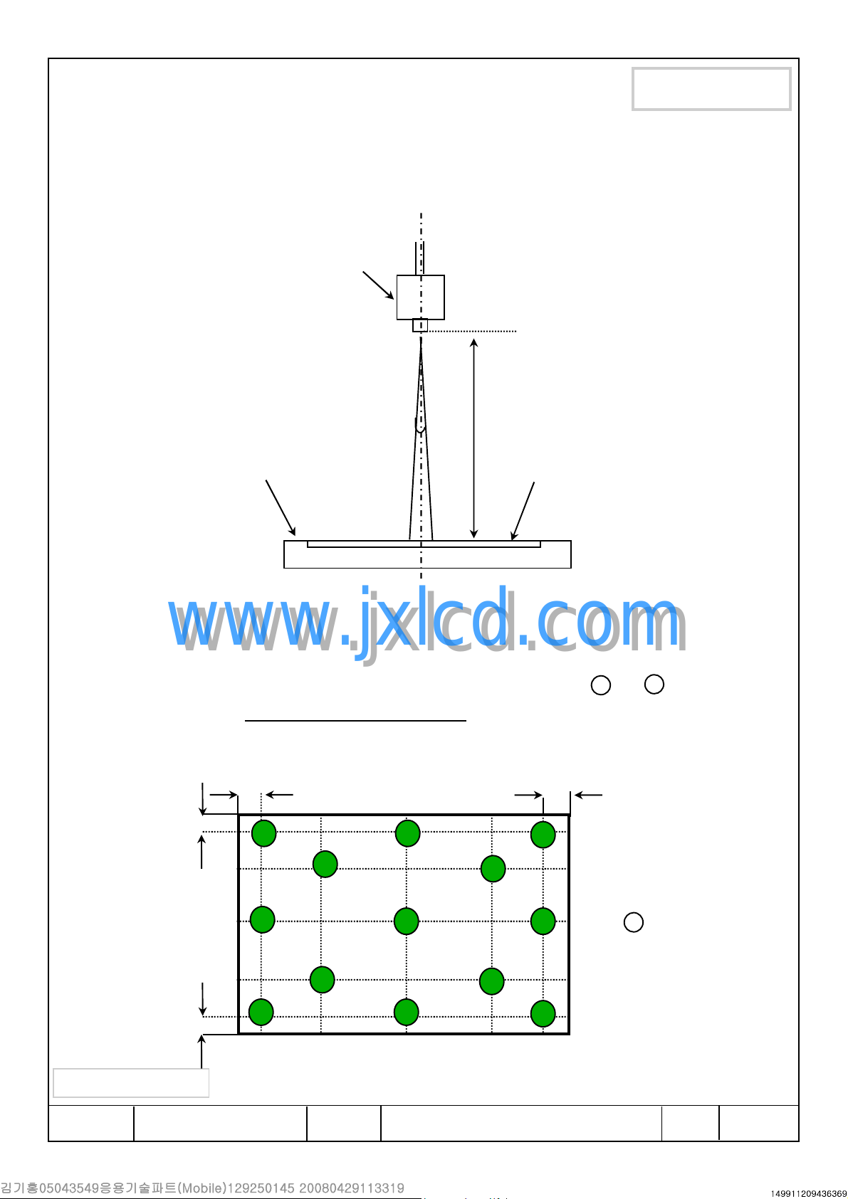
[ Optical characteristics measurement setup ]
www.jxlcd.com
www.jxlcd.com
Note 6) Definition of 13 points white variation (
Maximum luminance of 13 points
δL=
Minimum luminance of 13 points
10mm
10mm
13 12
420 840
10
δ
L
), CR variation( C
1260
LCD panel
VER
) [ ~ ]
1 13
10mm
11
9
236
8
5
3
10mm
Samsung Secret
Doc.No. Rev.No
7
4
2
04-A00-G-080429
6
473
709
(lines)
1
: test point
Page
/ 31LTN184KT01-A01
9
3. ELECTRICAL CHARACTERISTICS
3.1 TFT LCD MODULE
Approval
Ta= 25 ± 2°C
NoteUnitMax.Typ.Min.SymbolItem
Voltage of Power Supply
Differential Input
Voltage for LVDS
Receiver Threshold
Hsync Frequency
Main Frequency
Rush Current
Current of Power
Supply
Note (1) Display data pins and timing signal pins should be connected.( GND = 0V )
(2) fV= 60Hz, f
(3) Power dissipation pattern
www.jxlcd.com
www.jxlcd.com
*a) White Pattern *b) Mosaic Pattern
High
Low
White
DCLK
= 53.82 MHZ, VDD= 3.3V , DC Current.
DD
IH
IL
H
DCLK
RUSH
I
DD
V3.63.33.0V
V
CM
= +1.2VmV+100--V
mV---100V
Hz-60-fvVsync Frequency
KHz-58.5-f
2CHMHz-60.84-f
(4)A1.5--I
(2),(3)*amA-500(2),(3)*bmA-650-Mosaic
(2),(3)*cmA900780-V. stripe
VIEW AREA
Samsung Secret
Doc.No. Rev.No
Display Brightest Gray Level
Display Darkest Gray Level
04-A00-G-080429
Page
10
/ 31LTN184KT01-A01
 Loading...