

Samsung KS86P6308, KS86C6308 Datasheet

KS86C6308/P6308 PRODUCT OVERVIEW
1 PRODUCT OVERVIEW
SAM88RCRI PRODUCT FAMILY
Samsung's SAM88RCRI family of 8-bit single-chip CMOS microcontrollers offers a fast and efficient CPU, a wide
range of integrated peripherals, and various mask-programmable ROM sizes.
A dual address/data bus architecture and a large number of bit- or nibble-configurable I/O ports provide a flexible
programming environment for applications with varied memory and I/O requirements. Timer/counters with
selectable operating modes are included to support real-time operations. Many SAM88RCRI microcontrollers
have an external interface that provides access to external memory and other peripheral devices.
KS86C6308/P6308 MICROCONTROLLER
The KS86C6308/P6308 single-chip 8-bit microcontroller is fabricated using an advanced CMOS process. It is built
around the powerful SAM88RCRI CPU core.
Stop and Idle power-down modes were implemented to reduce power consumption. To increase on-chip register
space, the size of the internal register file was logically expanded. The KS86C6308 has 8 K bytes of program
memory on-chip.
Using the SAM88RCRI design approach, the following peripherals were integrated with the SAM88RCRI core:
— Five configurable I/O ports (32 pins)
— 20 bit-programmable pins for external interrupts
— 8-bit timer/counter and 16-bit timwe/counter with three operating modes
— Full speed low speed USB function
The KS86C6308/P6308 is a versatile microcontroller that can be used in a wide range of full/low speed USB
support general purpose applications. It is especially suitable for use as a keyboard with hub controller and is
available in a 64-pin SDIP and a 64-pin QFP package.
OTP
The KS86C6308 microcontroller is also available in OTP (One Time Programmable) version, KS86P6308.
KS86P6308 microcontroller has an on-chip 8-Kbyte one-time-programmable EPROM instead of masked ROM.
The KS86P6308 is comparable to KS86C6308, both in function and in pin configuration.
1-1

PRODUCT OVERVIEW KS86C6308/P6308 (Preliminary Spec)
FEATURES
CPU
• SAM88RCRI CPU core
Memory
• 8-KB Internal program memory(ROM)
• 256-byte internal register file
(160-byte:General Purpose)
Instruction Set
• 41 instructions
• IDLE and STOP instructions added for powerdown modes
Instruction Execution Time
• 332ns at 12 MHz f
OSC
Interrupts
• 32 interrupt sources with one vector, each
source has its pending bits
• One level, one vector interrupt structure
Oscillation Frequency
Timer A
• One 8-bit basic timer for watchdog function and
programmable oscillation stabilization
programmable 8-bit timer internal generation
function interval, capture, PWM mode
match/capture overflow interrupt
Timer B
• Programmable 16-bit timer interval generation
function interval, capture, PWM mode
match/capture overflow interrupt
Universal Serial Bus with HUB
• 1 upstream port
• 4 downstream port and one embedded function
each port supports separated enable LED builtin 3.3 V voltage regulator
USB/GPIO Function
• Upstream port
Operation Temperature Range
• - 40 °C to + 85 °C
• 12 MHz crystal/ceramic oscillator
• External clock source
General I/O
• Bit programmable five I/O ports (30 pins total)
1-2
Operation Voltage Range
• 4.0 V to 5.5 V
Package Types
• 64-pin SDIP
• 64-pin QFP
KS86C6308/P6308 (Preliminary Spec) PRODUCT OVERVIEW
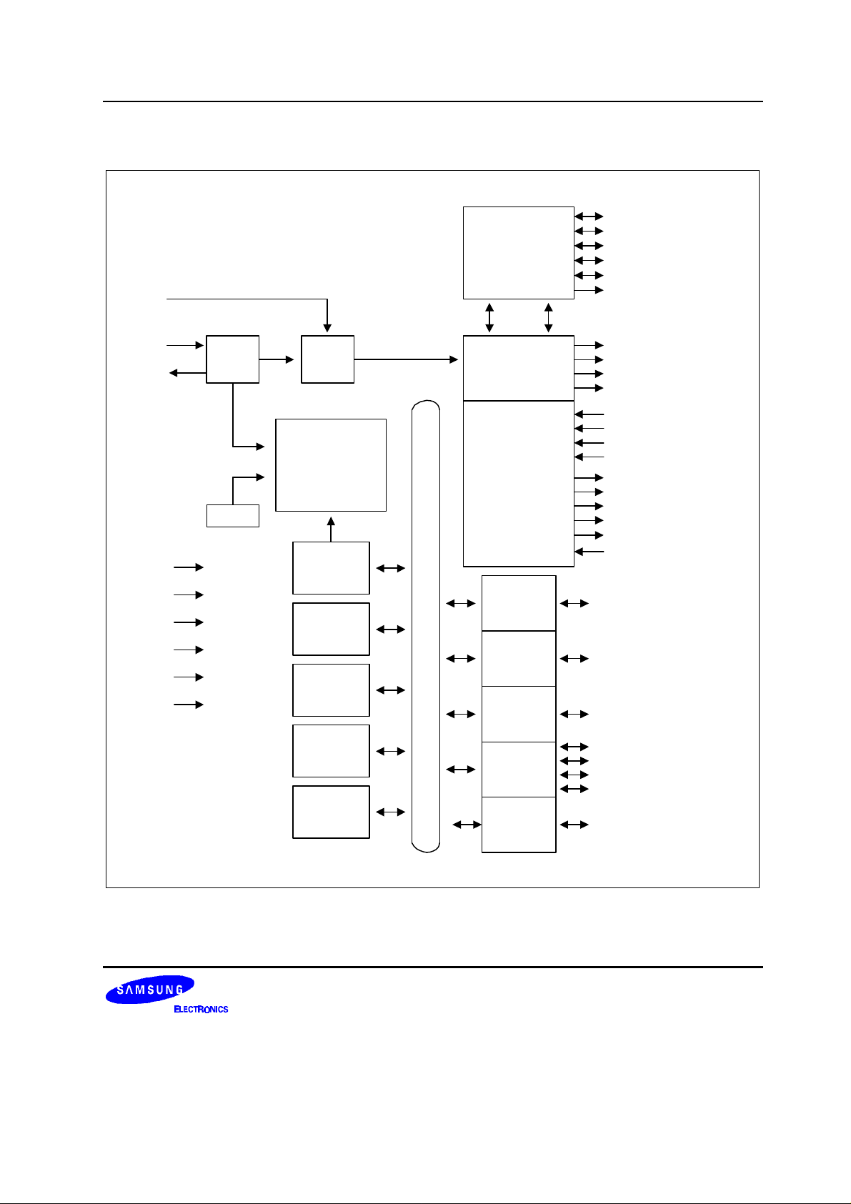
BLOCK DIAGRAM
DP0/GPIO, DM0/GPIO
DP1, DM1
DP2, DM2
DP3, DM3
DP4, DM4
3.3 V
OUT
PWREN1
PWREN2
PWREN3
PWREN4
OCDET1
OCDET2
OCDET3
OCDET4
LEDON0
LEDON1
LEDON2
LEDON3
LEDON4
GANGED
P0.0/INT2 - P0.7/INT2
P1.0 - P1.7
P2.0/INT0 - P2.7/INT0
LPF
12 MHz
XI
XO
V
DD
V
SS
V
SS1
TEST
RESET
TMOD
OSC
12 MHz
LVD
PLL
SAM88RCRI
CORE
8K
ROM
160 Byte
RAM
Timer A
(8 Bit)
48 MHz
USB Transceiver
&
Voltage Regulator
USB
Module
USB
Device
Control
8
B
Port
i
t
B
Port
U
S
Port
Timer B
(16 Bit)
Basic
Timer
Figure 1-1. Block Diagram
Port
Port
P3.3/TACLK/CLO
P3.2/TBCLK/USB_CLK
P3.1/TBCAP/TAOUT
P3.1/TACAP/TBOUT
P4.0/INT1
P4.1/INT1
1-3
PRODUCT OVERVIEW KS86C6308/P6308 (Preliminary Spec)
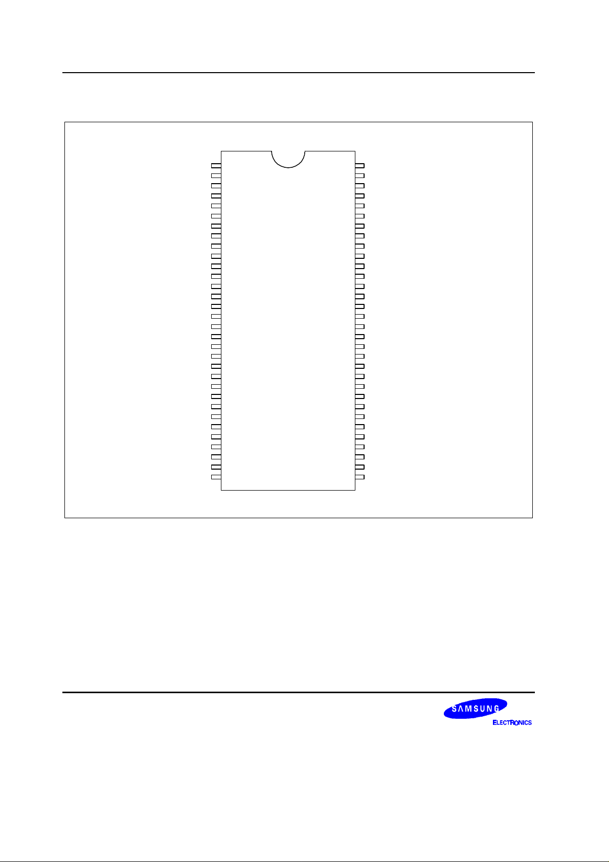
PIN ASSIGNMENTS
SDAT
SCLK
RESET
LEDON4
P1.4
P1.5
P1.6
P1.7
P4.0/INT1
P4.1/INT1
P2.0/INT0
P2.1/INT0
P2.2/INT0
P2.3/INT0
P2.4/INT0
P2.5/INT0
/P2.6/INT0
/P2.7/INT0
VDD
/VDD
VSS
/VSS
XO
XI
TEST
/TEST
VSS/V
/RESET
TMODE
DP0/GPIO
DM0/GPIO
DP1
DM1
DP2
DM2
DP3
DM3
/XO
/XI
LPF
SSA
10
11
12
13
14
15
16
17
18
19
20
21
22
23
24
25
26
27
28
29
30
31
32
1
2
3
4
5
6
7
8
9
KS86C6308/P6308
LEDON3
64
LEDPN2
63
LEDON1
62
LEDON0
61
OCDET4
60
PWREN4
59
P1.3
58
P1.2
57
P1.1
56
P1.0
55
P0.7/INT2
54
P0.6/INT2
53
P0.5/INT2
52
P0.4/INT2
51
P0.3/INT2
50
P0.2/INT2
49
P0.1/INT2
48
P0.0/INT2
47
OCDET3
46
PWREN
45
P3.3/TACLK/CLO
44
P3.2/TBCLK/USB_CLK
43
P3.1/TBCAP/TAOUT
42
P3.0/TACAP/TBOUT
41
V
SS1
/
40
39
38
37
36
35
34
33
V
OCDET2
PWREN2
ECDET1
PWREN1
3.3V
OUT
DM4
DP4
3
SS
1-4
Figure 1-2. Pin Assignment Diagram (64-Pin SDIP Package)
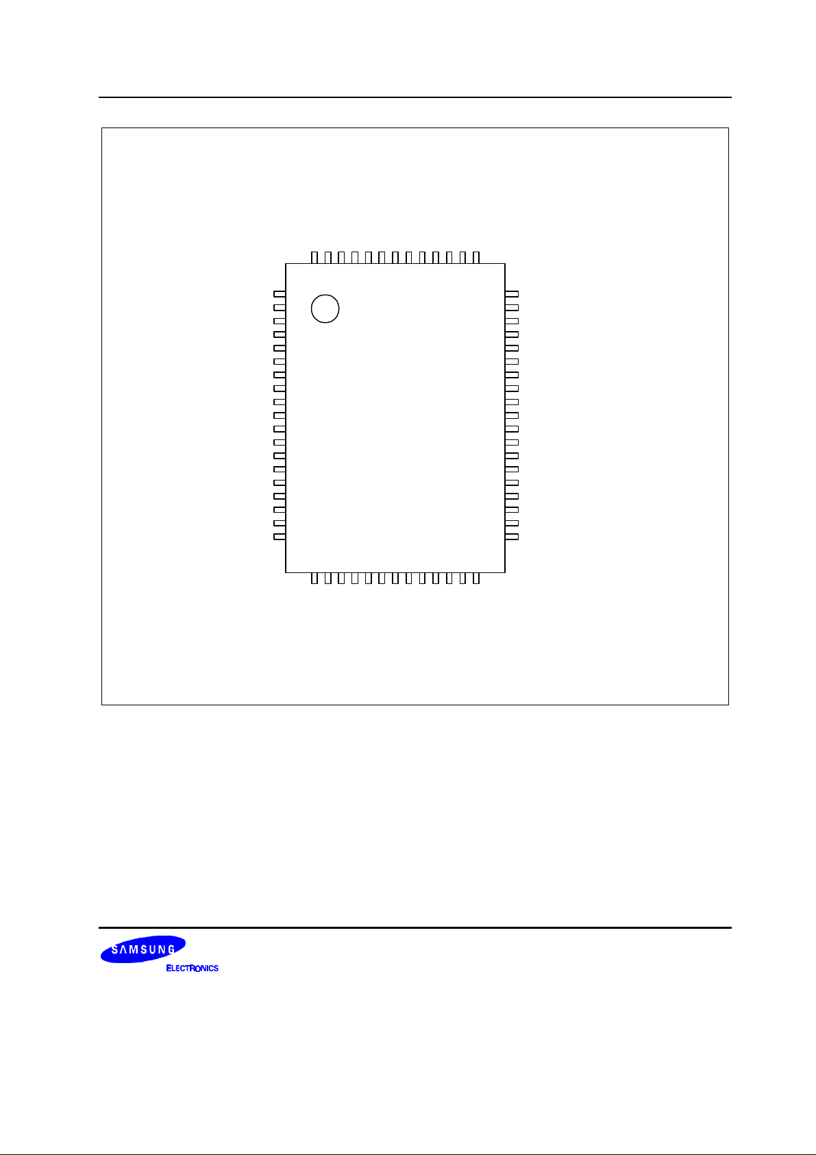
KS86C6308/P6308 (Preliminary Spec) PRODUCT OVERVIEW
P41/INT1
P40/INT1
P17
P16
P15
P14
LEDON4
LEDON3
LEDON2
LEDON1
LEDON0
OCDET4
PWREN4
64636261605958575655545352
SDAT
SCLK
RESET
P2.0/INT0
P2.1/INT0
P2.2/INT0
P2.3/INT0
P2.4/INT0
P2.5/INT0
/P2.6/INT0
/P2.7/INT0
VDD/V
VSS/V
XO
XI
TEST
/TEST
VSS/V
/RESET
TMODE
DP0/GPIO
DM0/GPIO
/XO
LPF
SSA
DD
/XI
SS
1
2
3
4
5
6
7
8
9
10
11
12
13
14
15
16
17
18
19
KS86C6308
(KS86P6308)
P1.3
51
P1.2
50
P1.1
43
P1.0
48
P0.7/INT2
47
P0.6/INT2
46
P0.5/INT2
45
P0.4/INT2
44
P0.3/INT2
43
P0.2/INT2
42
P0.1/INT2
41
P0.0/INT2
40
OCDET3
39
PWREN3
38
P3.3/TACLK/CLO
37
P3.2/TBCLK/USB_CLK
36
P3.1/TBCAP/TAOUT
35
P3.0/TACAP/TBOUT
34
GANGED
33
20212223242526272829303132
DP1
DP2
DP3
DM2
DM3
DP4
DM4
3.3VOUT
PWREN1
OCDET1
OCDET2
PWREN2
DM1
Figure 1-3. Pin Assignment Diagram (64-Pin QFP Package)
1-5
PRODUCT OVERVIEW KS86C6308/P6308 (Preliminary Spec)
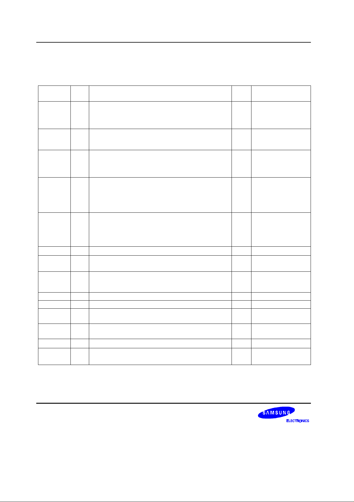
PIN DESCRIPTIONS
Table 1-1. KS86C6308/P6308 Pin Descriptions
Pin
Names
P0.0-P0.7 I/O
I/O Pin
Description
Bit-programmable I/O port for Schmitt trigger input or
Pin
Type
B INT2
open-drain output. Port 0 can be individually configured
as external interrupt inputs. Pull-up resistors are
assignable by software.
P1.0-P1.7 I/O Bit-programmable I/O port for Schmitt trigger input or
B –
open-drain output. Pull-up resistors are assignable by
software.
P2.0-P2.7 I/O Bit-programmable I/O port for Schmitt trigger input or
B INT0
open-drain output. Port 2 can also be individually
configured as external interrupt inputs. Pull-up resistors
are assignable by software.
P3.0-P3.3 I/O Bit-programmable I/O port for Schmitt trigger input, open-
drain output or push-pull output. Port 3 are designed for
to drive LED directly. P3.3 can be used to system clock
output(CLO) pin. P3.2 PLL clock out for PLL Block.
C
P3.3/TACLK/CLO
P3.2/TBCLK/
USB_CLK
P3.1/TBCAP/TAOUT
P3.0/TACAP/TBOUT
P4.0-P4.1 I/O Bit-programmable I/O port for Schmitt trigger input or
D INT1
open-drain output or push-pull output. Port4 can also be
individually configured as external interrupt inputs. In
output mode, pull-up resistors are assignable by
software. But in input mode, pull-up resistors are fixed.
3.3 V
X
X
OUT
INT0
INT1
INT2
OUT
IN
– 3.3 V output from internal voltage regulator – –
–
System clock input and output pin (crystal/ceramic
– –
oscillator, or external clock source)
I External interrupt for bit-programmable port0, port2 and
port4 pins when set to input mode.
– P2.0-P2.7
P4.0/P4.1
P0.0/P0.7
RESET I RESET signal input pin with LVD A –
LPF I Low Pass Filter Pin for PLL – –
TEST I
Test signal input pin (for factory use only; must be
– –
connected to VSS)
TMODE I Test signal input pin (for factory use only, must be
– –
connected to VSS)
V
DD
V
SS
V
SS1
– Power input pin – –
– VSS1 is a ground power for CPU core.
– –
VSS2 is a ground power for I/O and OSC block.
Share
Pins
1-6

KS86C6308/P6308 (Preliminary Spec) PRODUCT OVERVIEW
Table 1-1. KS86C6308/P6308 Pin Descriptions (Continued)
Pin
Names
DP1, DM1
I/O Pin
Description
I/O These pins are an USB Downstream pins. K –
DP2, DM2
DP3, DM3
DP4, DM4
DP0/GPIO
DM0/GPIO
I/O These pins are an USB Upstream pin, programmable
port for USB interface or General purpose I/O interface.
LEDON0 O Root port LED enable. N-channel open-drain output.
= 0 Turn LED ON. HUB not Suspend
= 1 Turn LED OFF. Reset, Suspend, Transfer in
progress
LEDON1-4 O Four downstream port LED enable. N-channel open-
drain output.
= 0 Turn LED ON. Port Enable and HUB not Suspend
= 1 Turn LED OFF. Reset, Suspend, Transfer in
progress
OCDET1-4 I Four downstream power sense
= 0 Over Current Detected
= 1 Power Okay
PWREN1-4 O
Power on/off control signals. PWREN1 - PWREN4 are
active low, N-CH open-drain outputs.
In GANGED mode, all output are swithed together.
GANGED I
Gang or Individual Power Control of downstream ports
= 0 Individual
= 1 Gang
Pin
Type
– –
G –
G –
F –
G –
F –
Share
Pins
1-7
PRODUCT OVERVIEW KS86C6308/P6308 (Preliminary Spec)
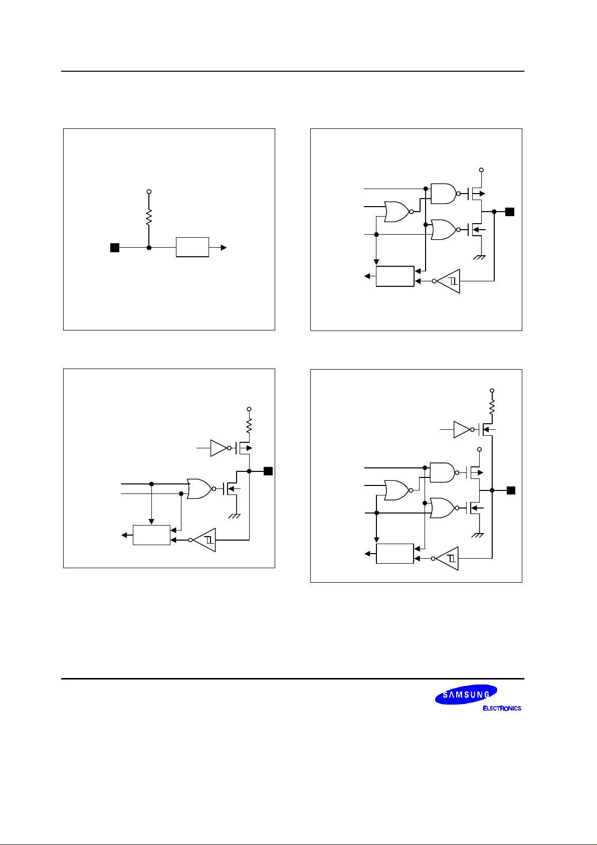
PIN CIRCUIT DIAGRAMS
VDD
V
DD
Output Data
Pull-up
Resistor
Noise
Filter
Figure 1-4. Pin Circuit Type A (RESET)
Pull-up Enable
Output Disable
Open Data
Input Data
D0
MUX D1
Pull-up
Resistor
VSS
VDD
Open Drain
Output
DIsable
Input Data
D0
MUX D1
Figure 1-6. Pin Circuit Type C (Port 3)
Resistor
Pull-up Enable
Output Data
Open Drain
Output
DIsable
Input Data
D0
MUX D1
V
Pull-up
V
V
DD
SS
SS
V
DD
Figure 1-5. Pin Circuit Type B (Port 0, 1, 2)
1-8
Figure 1-7. Pin Circuit Type D (Port 4)

KS86C6308/P6308 (Preliminary Spec) PRODUCT OVERVIEW
V
DD
Pull-up
Resistor
Figure 1-8. Pin Circuit Type F
3.0 V < V <3.6 V
Only on
Upstream Ports
DP
DM
X
X
15 KΩ ± 5 %
or
Equivalent
RXD
RXDP
Only on
Downstream
Ports
RXDM
TXDP
OEN
Speed (Only on Downstream Ports)
TXDM
15 KΩ ± 5 %
Figure 1-9. Pin Circuit Type K
1-9
 Loading...