

Samsung KS86C6104, KS86P6104 Datasheet

KS86C6104/P6104 PRODUCT OVERVIEW
1PRODUCT OVERVIEW
SAM87RI PRODUCT FAMILY
Samsung's SAM87RI family of 8-bit single-chip CMOS microcontrollers offer fast and efficient CPU, a wide range
of integrated peripherals, and supports OTP device.
A dual address/data bus architecture and bit- or nibble-configurable I/O ports provide a flexible programming
environment for applications with varied memory and I/O requirements. Timer/counters with selectable operating
modes are included to support real-time operations.
KS86C6104/P6104 MICROCONTROLLER
The KS86C6104/P6104 microcontroller with USB function can be used in a wide range of general purpose
applications. It is especially suitable for mouse or joystick controller and is available in 20-pin DIP and 24-pin
SOP package.
The KS86C6104/P6104 single-chip 8-bit microcontroller is fabricated using an advanced CMOS process. It is
built around the powerful SAM87RI CPU core.
Stop and Idle power-down modes were implemented to reduce power consumption. To increase on-chip register
space, the size of the internal register file was logically expanded. The KS86C6104/P6104 has 4 Kbytes of
program memory on-chip and 208 bytes of RAM including 16 bytes of working register.
Using the SAM87Ri design approach, the following peripherals were integrated with the SAM87Ri core:
— Two configurable I/O ports (11 pins)
— 7 bit-programmable pins for external interrupts
— 8-bit timer/counter with two operating modes
OTP
The KS86C6104 microcontroller is also available in OTP (One Time Programmable) version, KS86P6104.
KS86P6104 microcontroller has an on-chip 4-Kbyte one-time-programmable EPROM instead of masked ROM.
The KS86P6104 is comparable to KS86C6104, both in function and in pin configuration.
1-1

PRODUCT OVERVIEW KS86C6104/P6104
FEATURES
CPU
• SAM87RI CPU core
Memory
• 4-Kbyte internal program memory (ROM)
• 208-byte RAM
• 16 bytes of working register
Instruction Set
• 41 instructions
• IDLE and STOP instructions added for powerdown modes
Instruction Execution Time
• 1.0 µs at 6 MHz f
OSC
Interrupts
• 12 interrupt sources with one vector
• One level, one vector interrupt structure
Oscillation Circuit Options
• 6 MHz crystal/ceramic oscillator
• External clock source
General I/O
• 11 bit-programmable I/O pins
Timer/Counter
• One 8-bit basic timer for watchdog function and
programmable oscillation stabilization interval
generation function
• One 8-bit timer/counter with Compare/Overflow
counter
USB Serial Bus
• Compatible to USB low speed (1.5 Mbps) device
1.0 specification.
• Serial bus interface engine (SIE)
— Packet decoding/generation
— CRC generation and checking
— NRZI encoding/decoding and bit-stuffing
• Two 8-byte receive/transmit USB buffer
Operating Temperature Range
• – 40°C to + 85°C
Operating Voltage Range
• 4.0 V to 5.25 V
Package Types
• 20-pin DIP
• 24-pin SOP
Comparator
• 4-channel mode, 4-bit resolution
• 3-channel mode, external reference
low EMI design
1-2
KS86C6104/P6104 PRODUCT OVERVIEW
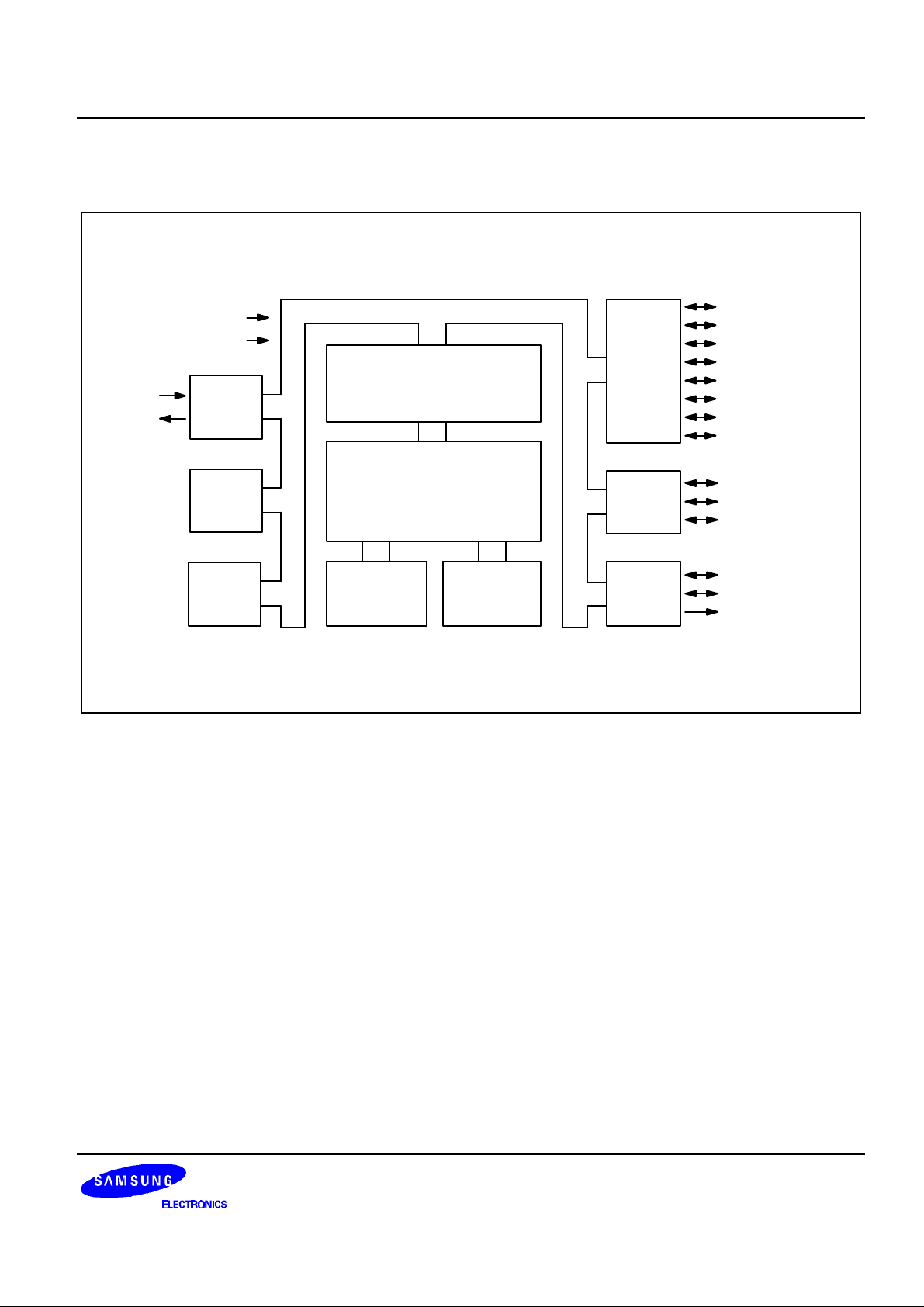
BLOCK DIAGRAM
X
X
IN
OUT
RESET
TEST
OSC
BASIC
TIMER
TIMER 0
I/O PORT AND
INTERRUPT CONTROL
SAM87RI
CPU
4-KB ROM
208-BYTE
REGISTER
Figure 1-1. Block Diagram
PORT 1/
COMPARATOR
PORT 0
USB
SIE
P1.0/CIN0/SCLK
P1.1/CIN1/SDAT
P1.2/CIN2
P1.3/CIN3
P1.4/INT1
P1.5/INT1
P1.6/INT1
P1.7/INT1
P0.0/INT0
P0.1/INT0
P0.2/INT0
D+
D-
3.3Vout
1-3
PRODUCT OVERVIEW KS86C6104/P6104
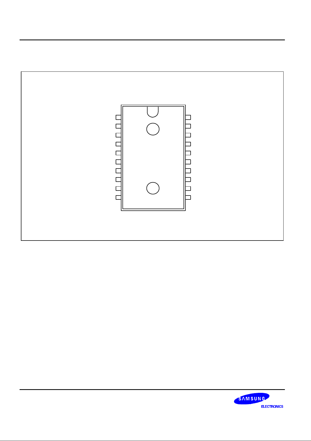
PIN ASSIGNMENTS
V
SS
X
out
X
TEST
P0.0/INT0
P0.1/INT0
RESET
P0.2/INT0
P1.7/INT1
P1.6/INT1
1
2
3
in
4
5
KS86C6104
6
(TOP VIEW)
7
8
9
10
20
19
18
17
16
15
14
13
12
11
V
DD
P1.0/CIN0
P1.1/CIN1
P1.2/CIN2
P1.3/CIN3
P1.4/INT1
P1.5/INT1
3.3V
out
D+
D-
Figure 1-2. Pin Assignment Diagram (20-Pin DIP Package)
1-4
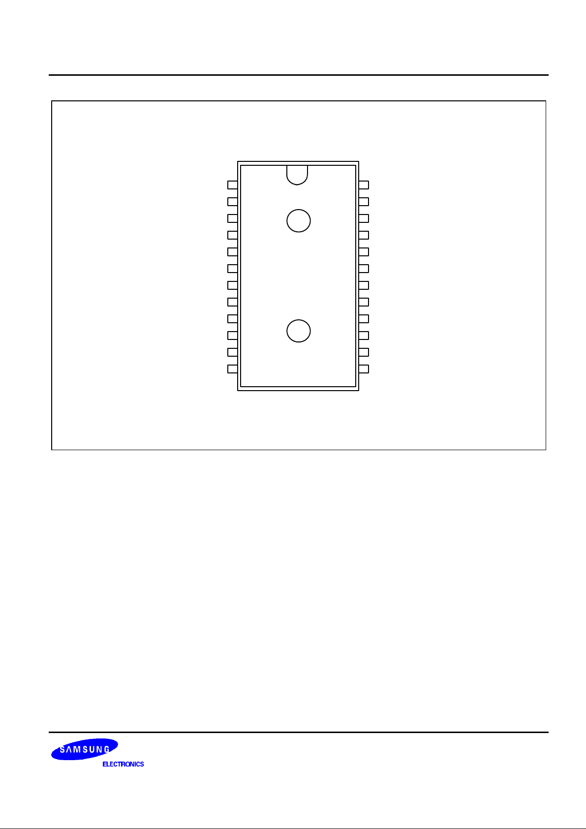
KS86C6104/P6104 PRODUCT OVERVIEW
V
SS
X
out
X
NC
TEST
P0.0/INT0
P0.1/INT0
RESET
NC
P0.2/INT0
P1.7/INT1
P1.6/INT1
1
2
3
in
4
5
6
KS86C6104
(TOP VIEW)
7
8
9
10
11
12
24
23
22
21
20
19
18
17
16
15
14
13
V
DD
P1.0/CIN0
P1.1/CIN1
NC
P1.2/CIN2
P1.3/CIN3
P1.4/INT1
P1.5/INT1
NC
3.3V
out
D+
D-
Figure 1-3. Pin Assignment Diagram (24-Pin SOP Package)
1-5

PRODUCT OVERVIEW KS86C6104/P6104
PIN DESCRIPTIONS
Table 1-1. KS86C6104/P6104 Pin Descriptions
Pin
Names
P0.0–P0.2 I/O Bit-programmable I/O port for Schmitt trigger
Pin
Type
Pin
Description
Circuit
Number
Pin
Numbers
D 5, 6, 8 INT0
input or push-pull output. Pull-up resistors are
individually assignable to input pins by software
and are automatically disable for output pins.
Port0 can be individually configured as external
interrupt inputs.
P1.0–P1.3 I/O Bit-programmable I/O port for Schmitt trigger
F-8 19–16 CIN0–
input or push-pull output. Pull-up resistors are
individually assignable to input pins by software.
Port1.0–1.3 can be configured as comparator
input
P1.4-P1.7 I/O Bit-programmable I/O port for Schmitt trigger
D 15, 14, 10, 9 INT1
input or push-pull output. Pull-up resistors are
individually assignable to input pins by software
and are automatically disabled for output pins.
Port1.4–1.7 can be individually configured as
external interrupt inputs.
D+/D- I/O Only used as USB tranceive/receive port. – 12–11 –
3.3VOUT O Internal regulator 3.3 V output pin for referencing
– 13 –
the voltage
XIN, X
OUT
– System clock input and output pin
– 3–2 –
(crystal/ceramic oscillator, or external clock
source)
INT0 I External interrupt for bit-programmable port0. D 5, 6, 8 Port0
INT1 I External interrupt for bit-programmable port1 D 9, 10, 14, 15 Port1
RESET
TEST I Test signal input pin (for factory use only; must
I RESET signal input pin. – 7 –
– 4 –
be connected to VSS)
Share
Pins
CIN3
1-6
V
DD
V
SS
– Power input pin – 20 –
– VSS is a ground power for CPU core. – 1 –
KS86C6104/P6104 PRODUCT OVERVIEW
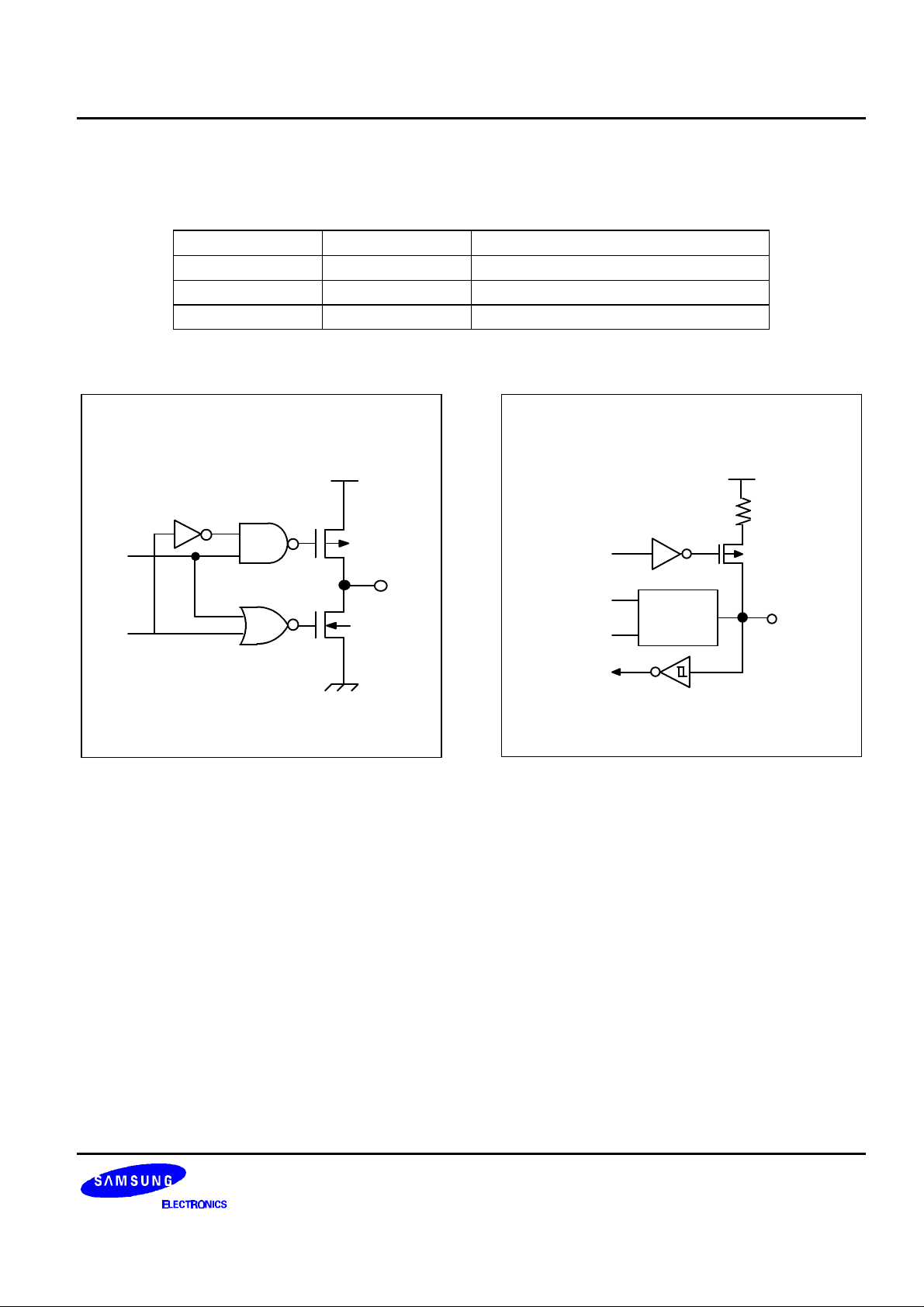
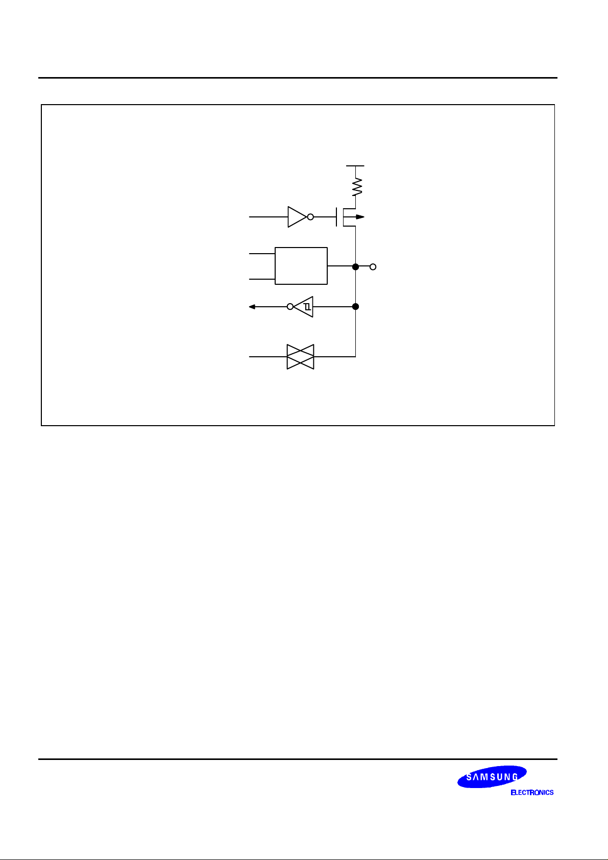
PIN CIRCUITS
Table 1-2. Pin Circuit Assignments for the KS86C6104/P6104
Circuit Number Circuit Type KS86C6104/P6104 Assignments
C O
D I/O Port0, Port1.4–1.7, INT0, INT1
F-8 I/O Port1.0–1.3
NOTE: Diagrams of circuit types C–D, and F-8 are presented below.
DATA
OUTPUT
DISABLE
V
DD
Figure 1-4. Pin Circuit Type C
OUT
V
PULL-UP
ENABLE
DATA
OUTPUT
DISABLE
CIRCUIT
TYPE C
Figure 1-5. Pin Circuit Type D
DD
IN/OUT
1-7
PRODUCT OVERVIEW KS86C6104/P6104
V
DD
PULL-UP
ENABLE
V
DD
DATA
OUTPUT
CIRCUIT
TYPE C
IN/OUT
DISABLE
ANALOG/
EXTERNAL
VREF INPUT
Figure 1-6. Pin Circuit Type F-8
1-8

KS86C6104/P6104 PRODUCT OVERVIEW
Right Button
CON_B
C3
X
X
V
V
IN
OUT
DD
SS
KS86P6104
P0.0/INT0
P0.1/INT0
Button
1 2 3
Left Button
Button
1 2 3
USB Cable
5
4
3
2
1
C4
R1
R2
C1 R3
C2
V3.3
D-
D+
RESET
P0.2/INT0
P1.7/INT1
P1.3/CIN3
P1.2/CIN2
P1.1/CIN1
P1.0/CIN0
5
4
3
Array 4
2
1
2
1
2
3
+
1
2
1
2
3
+
1
Figure 1-7. USB Mouse Circuit Diagram
1-9
 Loading...