

Samsung KS86C4302, KS86C4304, KS86P4304 Datasheet

KS86C4302/C4304/P4304 PRODUCT OVERVIEW
1 PRODUCT OVERVIEW
SAM87RI PRODUCT FAMILY
Samsung's SAM87Ri family of 8-bit single-chip CMOS microcontrollers offers a fast and efficient CPU, a wide
range of integrated peripherals, and various mask-programmable ROM sizes.
A address/data bus architecture and a large number of bit-configurable I/O ports provide a flexible programming
environment for applications with varied memory and I/O requirements. Timer/counters with selectable operating
modes are included to support real-time operations.
KS86C4302/C4304 MICROCONTROLLER
The KS86C4302/C4304 single-chip 8-bit microcontroller is fabricated using an advanced CMOS process. It is
built around the powerful SAM87Ri CPU core. The KS86C4302/C4304 is a versatile microcontroller, with its A/D
converter, timer, PWM, and SIO it can be used in a wide range of general purpose applications.
Stop and Idle power-down modes were implemented to reduce power consumption. To increase on-chip register
space, the size of the internal register file was logically expanded. The KS86C4302/C4304 have 2-Kbytes or 4Kbytes of program memory on-chip (ROM) and 112-bytes of general purpose register area RAM.
Using the SAM87Ri design approach, the following peripherals were integrated with the SAM87Ri core:
— Three configurable I/O ports (13 pins)
— Five interrupt sources with one vector and one interrupt level
— One 8-bit timer/counter with time interval mode
— Analog to digital converter with five input channels and 10-bit resolution
— One synchronous SIO module
— One 12-bit PWM output
The KS86C4302/C4304 microcontroller is ideal for use in a wide range of electronic applications requiring simple
timer/counter, PWM, ADC, and SIO. KS86C4302/C4304 is available in a 20/18/16-pin DIP and a 20-pin SOP
package.
OTP
The KS86P4304 is an OTP (One Time Programmable) version of the KS86C4302/C4304 microcontroller. The
KS86P4304 has on-chip 4-Kbyte one-time-programmable EPROM instead of masked ROM. The KS86P4304 is
fully compatible with the KS86C4302/C4304, in function, in D.C. electrical characteristics and in pin configuration.
1-1

PRODUCT OVERVIEW KS86C4302/C4304/P4304
FEATURES
CPU
• SAM87RI CPU core
Memory
• 2/4-Kbyte internal program memory (ROM)
• 112-byte general purpose register area (RAM)
Instruction Set
• 41 instructions
• The SAM87RI core provides all the SAM87 core
instruction except the word-oriented instruction,
multiplication, division, and some one-byte
instruction.
Instruction Execution Time
• 600 ns at 10 MHz f
• 375 ns at 16 MHz f
(minimum cycles)
OSC
(minimum cycles)
OSC
Interrupts
• 5 interrupt sources with one vector and one level
interrupt structure
Timer/Counters
• One 8-bit basic timer for watchdog function
• One 8-bit timer/counter for the time interval
mode
PWM Module
• 12-bit PWM 1-ch (Max: 250 kHz)
• 6-bit base + 6-bit extension frame
A/D Converter
• Five analog input pins
• 10-bit conversion resolution
Buzzer Frequency Range
• 200 Hz to 20 kHz signal can be generated
Oscillation Frequency
• 1 MHz to 16 MHz external crystal oscillator
• Maximum 16 MHz CPU clock
• 4 MHz RC oscillator
General I/O
• Two I/O ports (Toatal 13 pins)
• One output only port (port 2)
• Bit programmable ports
Serial I/O
• One synchronius serial I/O module
• Selectable transmit and receive rates
Built-in reset Circuit (LVD)
• Low voltage detector for safe reset
Operating Temperature Range
• - 40°C to + 85°C
Operating Voltage Range
• 3.0 V to 5.5 V
OTP Interface Protocol Spec
• Serial OTP
Package Types
• 20-pin DIP-300
• 20-pin SOP-375
• 18-pin DIP-300
• 16-pin DIP-300
1-2
KS86C4302/C4304/P4304 PRODUCT OVERVIEW
SCK (P1.3 or P2.0)
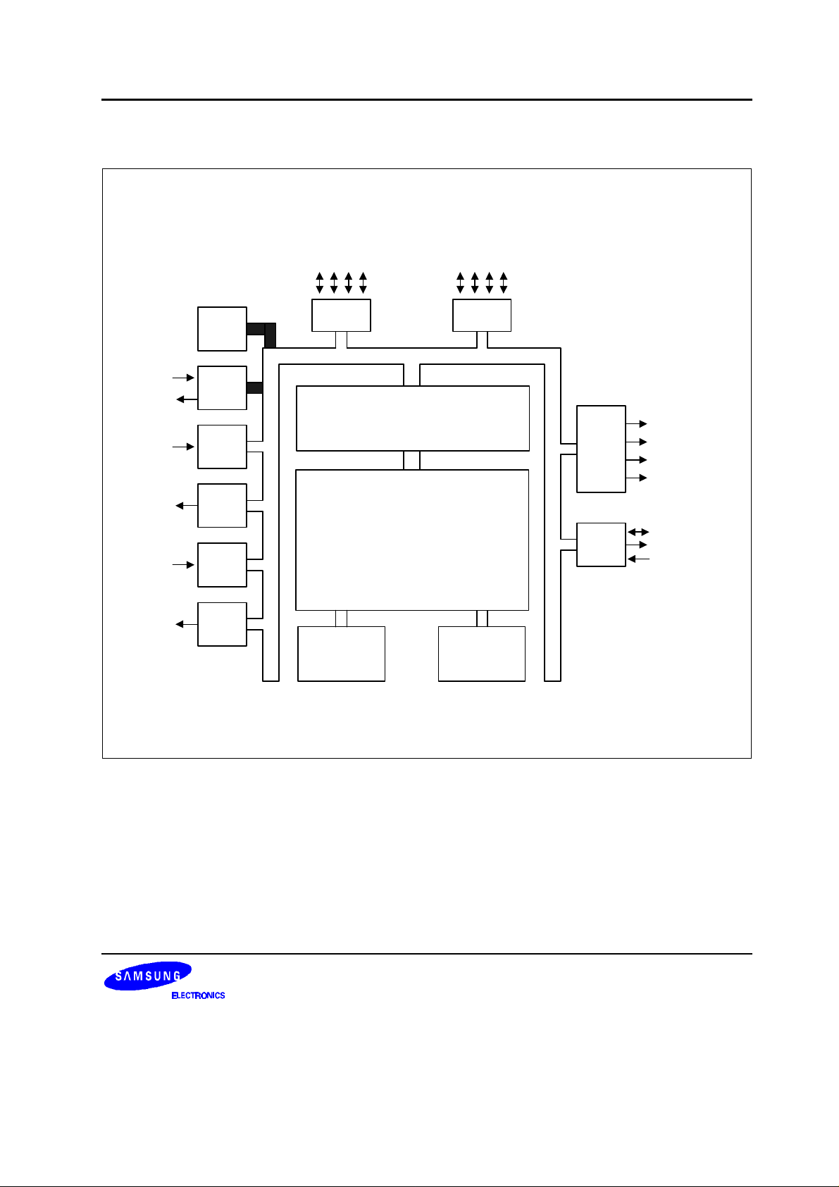
BLOCK DIAGRAM
X
X
OUT
P0.2/T0CK
P0.0/BUZ
ADC0-ADC4
P0.1/PWM
P0.0-P0.3
BUZ, PWM, INT0, INT1
Basic
Timer
IN
OSC
Port 0 Port 1
P1.0-P1.4
ADC0-ADC4
SCK, SO, SI, CLO
I/O Port and
P2.0/SCK
P2.1/SO
P2.2
P2.3
SO (P1.2 or P2.1)
SI (P1.1)
Timer 0
BUZ
ADC
PWM
2-KB ROM
4-KB ROM
Interrupt Control
SAM87RI CPU
Port 2
SIO
112-Byte
Register File
Figure 1-1. Block Diagram
1-3
PRODUCT OVERVIEW KS86C4302/C4304/P4304
PIN ASSIGNMENTS
V
V
SS
X
X
OUT
TEST
P0.2/T0CK/INT0
P0.1/PWM
RESET
P0.0/BUZ
P2.0/SCK
1
IN
2
3
4
5
KS86C4302/
6
4304
20
19
18
17
16
15
(TOP VIEW)
7
8
9
14
13
12
DD
P0.3/INT1
P1.0/ADC0
P1.1/ADC1/SI
P1.2/ADC2/SO
P1.3/ADC3/SCK
P1.4/ADC4/CLO
AV
REF
P2.1/SO
P2.3
P2.2
10
11
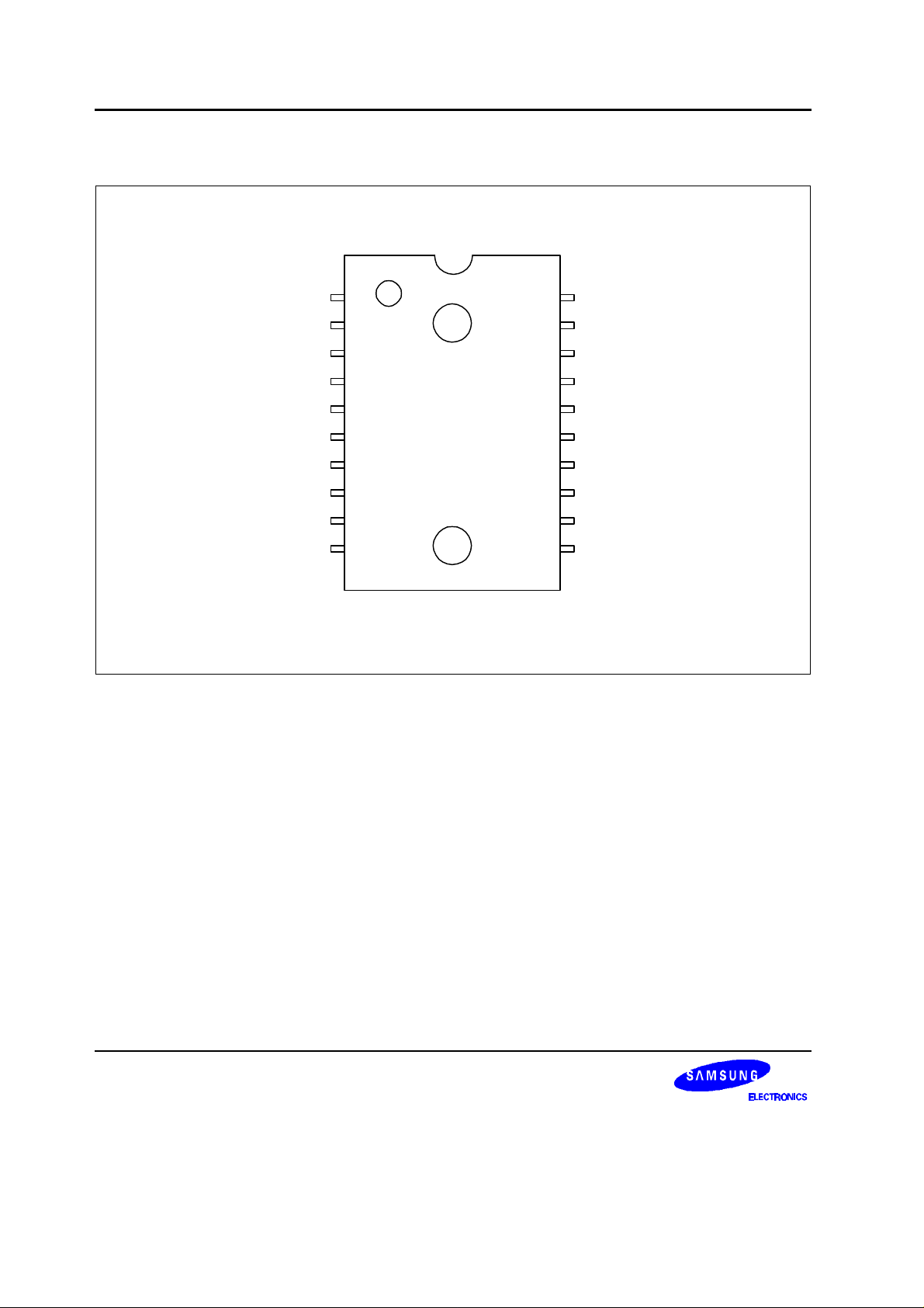
Figure 1-2. Pin Assignment Diagram (20-Pin DIP Package)
1-4
KS86C4302/C4304/P4304 PRODUCT OVERVIEW
V
SS
V
X
OUT
X
TEST
P0.2/T0CK/INT0
P0.1/PWM
1
IN
2
3
4
5
KS86C4302/
6
4304
20
19
18
17
16
15
DD
P0.3/INT1
P1.0/ADC0
P1.1/ADC1/SI
P1.2/ADC2/SO
P1.3/ADC3/SCK
(TOP VIEW)
P1.4/ADC4/CLO
RESET
P0.0/BUZ
P2.0/SCK
P2.2
7
8
9
10
14
13
12
11
REF
AV
P2.1/SO
P2.3
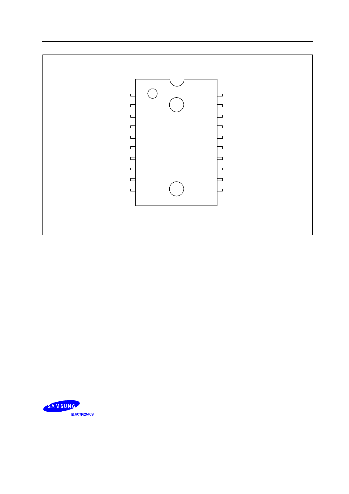
Figure 1-3. Pin Assignment Diagram (20-Pin SOP Package)
1-5
PRODUCT OVERVIEW KS86C4302/C4304/P4304
V
SS
V
X
OUT
X
TEST
P0.2/T0CK/INT0
P0.1/PWM
RESET
P0.0/BUZ
P2.0/SCK
1
IN
2
3
4
KS86C4302/
5
6
4304
(TOP VIEW)
7
8
9
18
17
16
15
14
13
12
11
10
DD
P0.3/INT1
P1.0/ADC0
P1.1/ADC1/SI
P1.2/ADC2/SO
P1.3/ADC3/SCK
P1.4/ADC4/CLO
AV
REF
P2.1/SO
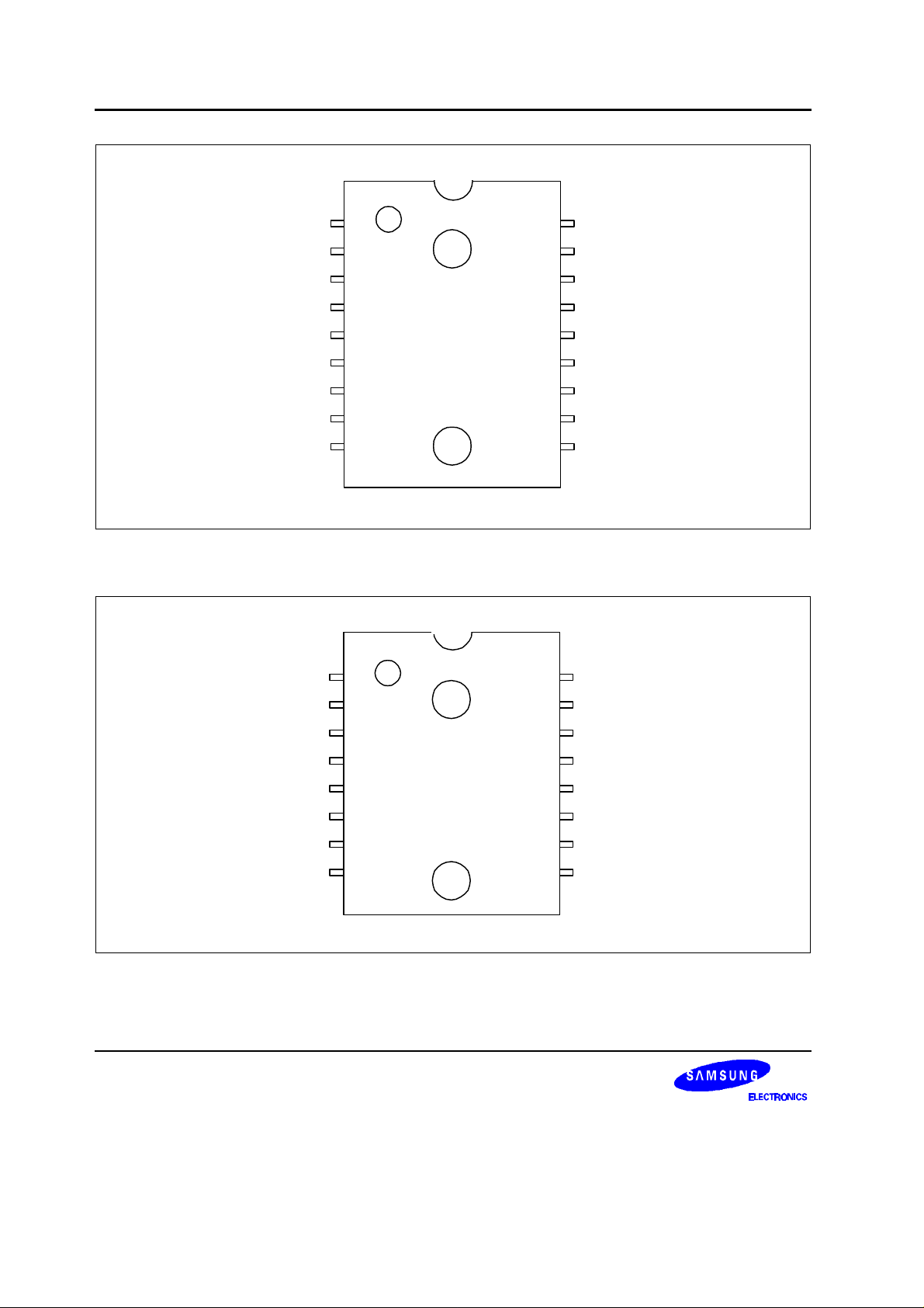
Figure 1-4. Pin Assignment Diagram (18-Pin DIP Package)
V
SS
X
X
OUT
TEST
1
IN
2
3
KS86C4302/
4
16
15
14
13
4304
P0.2/T0CK/INT0
P0.1/PWM
RESET
P0.0/BUZ
5
(TOP VIEW)
6
7
8
Figure 1-5. Pin Assignment Diagram (16-Pin DIP Package)
12
11
10
9
V
DD
P0.3/INT1
P1.0/ADC0
P1.1/ADC1/SI
P1.2/ADC2/SO
P1.3/ADC3/SCK
P1.4/ADC4/CLO
AV
REF
1-6
KS86C4302/C4304/P4304 PRODUCT OVERVIEW
PIN DESCRIPTIONS
Table 1-1. KS86C4302/C4304 Pin Descriptions
Pin
Names
P0.0-P0.3 I/O
P1.0-P1.4 I/O Bit-programmable I/O port for Schmitt trigger
Pin
Type
Pin
Description
Bit-programmable I/O port for Schmitt trigger
input or push-pull, open-drain output. Pull-up
resistors are assignable by software. Port 0 pins
can also be used as alternative function.
input or push-pull, open-drain output. Pull-up
resistors are assignable by software. Port 1 pins
can also be used as alternative function.
Circuit
Type
Share
Pins
E BUZ
PWM
INT0/T0CK
INT1
E-1 ADC0-ADC4
SI
SO
SCK
CLO
P2.0-P2.3 O Push-pull or open-drain output port. Pull up
resistors are assignable by software. Port 2.0-2.1
E-2 SCK
SO
pins can also be used as alternative function.
XIN, X
OUT
–
Crystal/ceramic, or RC oscillator signal for
– –
system clock.
RESET
TEST I Test signal input pin (for factory use only: must be
I System RESET signal input pin. B –
– –
connected to VSS)
V
DD, VSS
AV
REF
AV
SS
SCK I/O Serial interface clock I/O E-1
SO O Serial data output E-1
– Voltage input pin and ground – –
– A/D converter reference voltage input and ground – –
Bonded to VSS internally
P1.3 or
E-2
P2.0
P1.2 or
E-2
P2.1
SI I Serial data input E-1 P1.1
CLO O System clock output port E-1 P1.4
BUZ O 200 Hz- 20 kHz frequency output for buzzer sound E P0.0
PWM O 12-bit PWM output E P0.1
INT0-INT1 I External interrupt input port E P0.2
P0.3
T0CK I Timer 0 external clock input E P0.2
ADC0-ADC4 I A/D converter input E-1 P1.0-P1.4
1-7
PRODUCT OVERVIEW KS86C4302/C4304/P4304
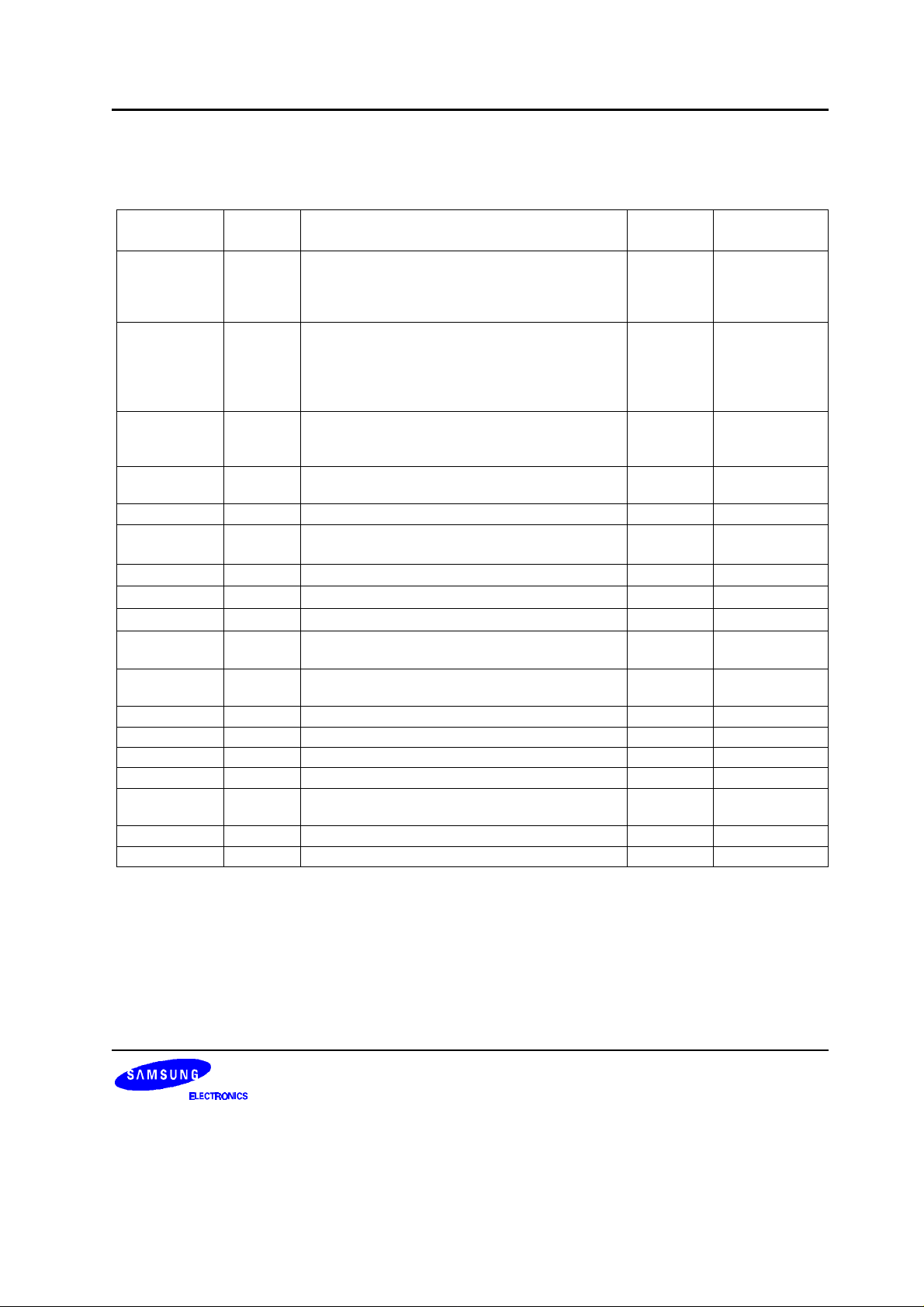
PIN CIRCUITS
V
DD
V
DD
P-Channel
In
N-Channel
Figure 1-6. Pin Circuit Type A
DD
V
Pull-Up
Resistor
In
Data
Output
DIsable
Pull-up
Enable
Output
DIsable
Figure 1-8. Pin Circuit Type C
V
DD
Data
Circuit
Type C
P-Channel
Out
N-Channel
P-Channel
I/O
1-8
Figure 1-7. Pin Circuit Type B
Data
Figure 1-9. Pin Circuit Type D
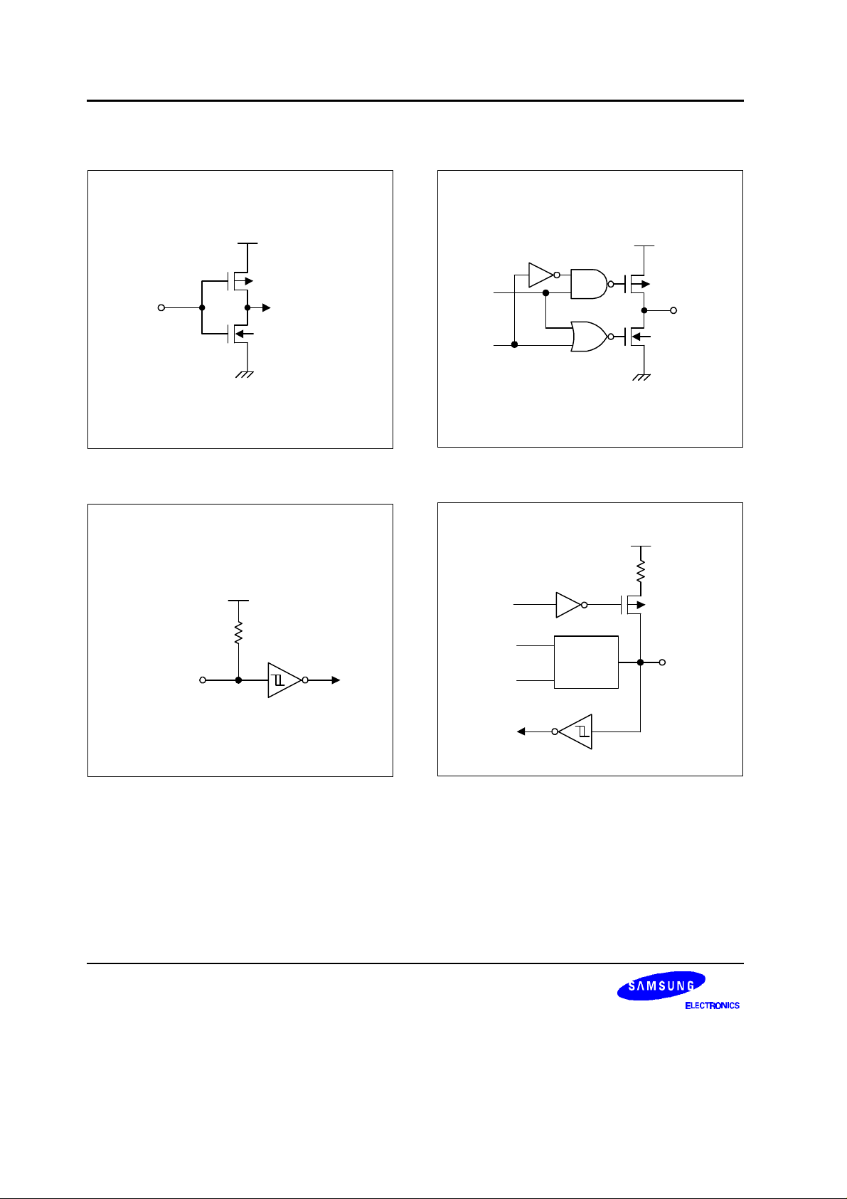
KS86C4302/C4304/P4304 PRODUCT OVERVIEW
DIsable
DIsable
DIsable
V
DD
DD
Open-Drain
Pull-up
V
DD
Resistor
Open-Drain
V
Pull-up
DD
V
Resistor
Output
Data
Output
Input
Open-Drain
Output
Data
Output
P-CH
N-CH
Figure 1-10. Pin Circuit Type E
DD
V
V
DD
P-CH
N-CH
Pull-up
Enable
I/O
Pull-up
Resistor
Pull-up
Enable
I/O
Output
Data
Output
P-CH
N-CH
Figure 1-12. Pin Circuit Type E-2
Pull-up
Enable
I/O
Digital
Input
Analog
Input
Figure 1-11. Pin Circuit Type E-1
1-9

PRODUCT OVERVIEW KS86C4302/C4304/P4304
NOTES
1-10

KS86C4302/C4304/P4304 ELECTRICAL DATA
14 ELECTRICAL DATA
OVERVIEW
In this section, the following KS86C4302/C4304 electrical characteristics are presented in tables and graphs:
— Absolute maximum ratings
— D.C. electrical characteristics
— A.C. electrical characteristics
— Input Timing Measurement Points
— Oscillator characteristics
— Oscillation stabilization time
— Operating Voltage Range
— Schmitt trigger input characteristics
— Data retention supply voltage in Stop mode
— Stop mode release timing when initiated by a RESET
— A/D converter electrical characteristics
— LVD circuit characteristics
— LVD reset Timing
— Serial I/O timing characteristics
— Serial data transfer timing
14-1
 Loading...