Samsung KS8630D Datasheet

PRELIMINARY
ENHANCED CALLING LINE IDENTIFIER WITH CALL WAITING KS8630D
BRIEF DESCRIPTION
16-SOP-225
KS8630D is a Low power mixed signal CMOS integrated circuit
for receiving a physical layer signals used in the Calling Line
Identification Presentation (CLIP) of British Telecom system,
the Calling Identity Delivery(CID) of Bellcore system, and
similar evolving systems before the call is put through. It can
also satisfy the requirements of CIDCW (Calling Identity
Delivery on Call Waiting) services including very high precision
detection of CAS (CPE Alerting Signal) tone and the signals
used in similar services when the call has already been put
through.
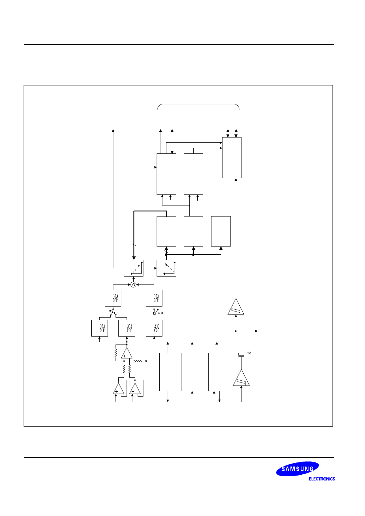
KS8630D carries out the following features : Ring or Line-reversal detection, CAS ( 2130Hz and 2750Hz) Tone
detection, and 1200-baud FSK demodulation which simultanesouly satisfies the BELL202 and the CCITT ( ITU-T )
V.23 specification. The demodulated data for Caller Identification is transmitted serially to the related u-controller.
KS8630D using a patented digital algorithm to detect demodulated FSK signals and CAS signal detection.
The device also has a built-in Automatic Gain Control circuitry which is capable of very high precision detection of
CAS tone. It is suitable for use in Adjunct Boxes or Feature Phones with CID / CIDCW applications.
FEATURES
• CID and CIDCW System Operation
• High Performance CAS Detection and Loop State Tone Alert signal detection
• Internal Automatic Gain Control circuitry for the high precision CAS detection
• Digital Logic FSK demodulator
• Ring or Line-polarity reversal detection
• Low power consumption in standby mode
• 3.58MHz crystal oscillator
• 3.3V ~ 5V Operation
• 16-SOP package ( 225Mil )
APPLICATIONS
• CID / CIDCW Adjunct Boxes and Feature Phones
• A system for British Telecom, Bellcore, CCA
• Computer Telephone Integrated system
• Call Logging Systems
• Voice-Mail Equipment
ORDERING INFORMATION
Device Package Operating Temperature
KS8630 16-SOP-225 0°C ~ 70°C
1

PRELIMINARY
RTB
XOUT
KS8630D ENHANCED CALLING LINE IDENTIFIER WITH CALL WAITING
BLOCK DIAGRAM
TO/FROM MICROCONTROLLER
OFFHOOK
AGC_VB
5
AGC
DATA
DCLK
FSK
DEMODULATOR
GAIN
CONTROL
8
ADC
TONE
DISCRIMINATOR
PEAK
DETECTOR
MODE
MODE &
INTERRUPT
LEVEL
DETECTOR
INTB
GENERATOR
BPF
LPF
INN
BPF
INP
LPF
BPF
BIAS
GENERATOR
VREF
BLOCK
SENSING
VOLTAGE
PD
Figure 1. KS8630D Block Diagram
CLOCK GEN
OSCILLATOR &
XIN
RD
2

PRELIMINARY
ENHANCED CALLING LINE IDENTIFIER WITH CALL WAITING KS8630D
PIN DIAGRAM
V
DD
AGC_VB
I
NN
I
NP
V
REF
RD
RTB
PD
1
2
3
16
15
14
KS8630D
4
5
6
7
8
Figure 2. KS8630D Pin Diagram
13
12
11
10
9
XOUT
XIN
INTB
DCLK
OFFHOOK
MODE
DATA
V
SS
3

PRELIMINARY
KS8630D ENHANCED CALLING LINE IDENTIFIER WITH CALL WAITING
PIN DESCRIPTION
Pin No. Pin Name Type Description
1 V
DD
P Positive Power Supply.
2 AGC_VB O AGC block bias terminal. Usually a 0.47uF capacitor is connected between this
3 I
4 I
5 V
NN
NP
REF
pin and V
I Inverting input of the on-chip input signal amplifier.
I Non-inverting input of the on-chip input signal amplifier.
O Reference Voltage. Typically 0.1 ~ 1uF is connected to GND.
pin to reduce a dc offset produced by internal circuitry.
REF
6 RD I(S) Schmitt trigger input to detect the ringing signal, ring-burst signal, Line-polarity
reversal signal.
7 RTB I(S)/O Open drain output/Schmitt trigger input.
An external resistor to V
and a capacitor to VSS should be connected with
DD
RTB to filter and to extend the RD input signal. Each components value is
related to the schmitt trigger input threshold and input signal frequency.
8 PD I(S) Power Down. Schmitt trigger & voltage sensing input.
If set to high level, all circuitry goes to power down mode except ring detection
& mode selection block. In order to satisfy the BT or Bellcore specification, it is
recommended to add a different application circuits.
All digital block can be resetted by this pin control. Whenever the u-controller
unmutes handset and enables keypad in Off-Hook state, KS8630D must
receive a reset pulse by this pin from microcontroller.
9 V
SS
P Negative Power Supply.
10 DATA B Demodulated FSK data output. Default state is a logic high level.
DATA is tranmitted serially to the microcontroller ( 8bit /unit, LSB first ).
DCLK is used for sync clock of this DATA.
In case of using this pin as input, it is used for testing of KS8630D functionality.
11 MODE B Mode output signal to show the current status ( Ring / Dual Tone / FSK signal
receiving). Default state is a logic high level.
If detects a CAS tone, this MODE pin will be set to logic low level during a pre-
determined timming. If detects a Ring or FSK signal, this pin will be set to high
level. With the INTB pin, it can be informed current status to microcontroller.
In case of using this pin as input, it is used for testing of KS8630D functionality.
12 OFFHOOK I Hook Status Input. If set to high level, the operation condition of KS8630D go
to the Off-Hook state. If set to low level, it goes to the On-Hook state.
13 DCLK B Synchronous clock output of DATA. Default state is logic high level.
The right data is in falling edge of this clock. In case of using this pin as input,
it is used for testing of KS8630D functionality
4

PRELIMINARY
ENHANCED CALLING LINE IDENTIFIER WITH CALL WAITING KS8630D
PIN DESCRIPTION (Continued)
Pin No. Pin Name Type Description
14 INTB O Interrupt output signal. It is an active low output that may be used as an
Interrupt Request / Wake-up signal to the microcontroller.
In case of ringing or line polarity reversal detection, dual tone detection and the
mark signal detection of FSK data, it will be activated.
With the MODE pin, it indicates current status to the microcontroller.
15 XIN I The input of the 3.58MHz on-chip crystal oscillator inverter.
16 XOUT O The output to the 3.58MHz on-chip crystal oscillator inverter.
NOTES:
I = Input
I(S) = Schmitt trigger Input
O = Output
B = Bidirectional I/O
5

PRELIMINARY
TO/FROM MICROCONTROLLER
KS8630D ENHANCED CALLING LINE IDENTIFIER WITH CALL WAITING
TYPICAL APPLICATION CIRCUIT
VDD
16
15
14
13
12
11
10
9
XOUT
XIN
INTB
DCLK
OFFHOOK
MODE
DATA
VSS
C1
X1
C2
TIP
RING
C7
C8
R1
R2
D3
D4
C3
C4
D1
D2
VDD
R3
R5
R6
C10
R4
C9
VDD
1
C6C5
R10
R7
AGC_VB
VDD
R8
VREF
R9
INN
INP
RD
RTB
PD
2
3
4
5
6
7
8
KS8630D
Note 1
C11
Note 2
R11
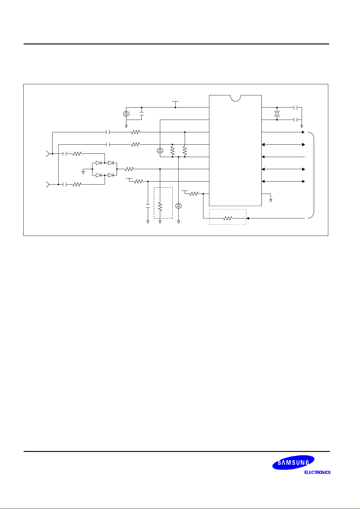
Figure 3. Recommended Typical Application Circuit Components
R1, R2, R3 470kΩ C1, C2 10pF
R4 150kΩ C3, C4 22nF
R5, R6, R7, R8 100kΩ C5 10µF
R9 82kΩ C6, C7, C8 100nF
R10 56kΩ C9 0.47µF
(Note 1) C10 220nF
R11 47kΩ
C11 0.1µF
(Note 2.)
X1 3.579545MHz
D1, D2, D3, D4 1N4004
NOTES:
1. When applying to the BT system, change R10 to 330kΩ to detect the Line Reversal signal.
2. When applying to the BT system, insert a resistance between the MCU’s PD related pin and KS8630D PD pin
(Refer to Section 1.6).
6

PRELIMINARY
ENHANCED CALLING LINE IDENTIFIER WITH CALL WAITING KS8630D
GENERAL DESCRIPTION
KS8630D is suitable for use in both system to British Telecom specificatios and BELLCORE specifications.
KS8630D to be used in different systems, the predetermined signals must be applied to the PD (pin#8) and the
OFFHOOK ( pin#12), which are defined by the application circuits or the microcontroller.
All detection modes related to the PD pin and the OFFHOOK pin are listed below:
PD OFFHOOK DETECTION MODE (Note1) REMARK
L L FSK Demodulation BELLCORE
L H Dual Tone Detection →
FSK Demodulation
SYSTEM
(Note2)
1/3 * V
1/3 * V
DD
DD
L Dual Tone Detection →
FSK Demodulation
H Dual Tone Detection →
BT SYSTEM
(Note3)
FSK Demodulation
H L Ringing or Line reversal Detection
H H −
Table 1. A Status of each detection mode
NOTES:
1. If a false reponse (talk-off) occurs or microcontroller receives FSK data, microcontroller should send low edge pulse
(with 10us duration timming approximately) to the PD pin.
Then, KS8630D will be re-initialized to the dual tone(CAS) detection mode.
2. If KS8630D is used in the BELLCORE system, a pull-up resistor should be inserted between the PD pin and VDD.
3. If KS8630D is used in the BT system, a pull-up resistor should be inserted between the PD pin and VDD.
In this case, a resistor should be inserted between KS8630D’s PD pin and microcontroller’s PD related pin.
Then, the voltage level of KS8630D’s PD pin will be 1/3*VDD when microcontroller's PD related pin set to low state.
7
 Loading...