

Samsung KS8620N, KS8620D Datasheet
KS8620
1 Chip CODEC for Digital Answering phone
INTRODUCTION
The KS8620 consists of on-chip PCM encoders, decoders
(PCM CODECs) and PCM line filter. This device
provide all the functions required to interface a fullduplex voice telephone circuit, digital answering phone.
This device is designed to perform the transmit encoding
and receive decoding as well as the transmit and receive
filtering function in PCM system. Also it is intended to be
used at the analog termination of a PCM line / trunk.
This device provide the Band pass filtering of the analog
signals prior to encoding and after decoding. This
combination device performs the encoding and decoding
of voice and call progress tones as well as the signaling
and supervision information.
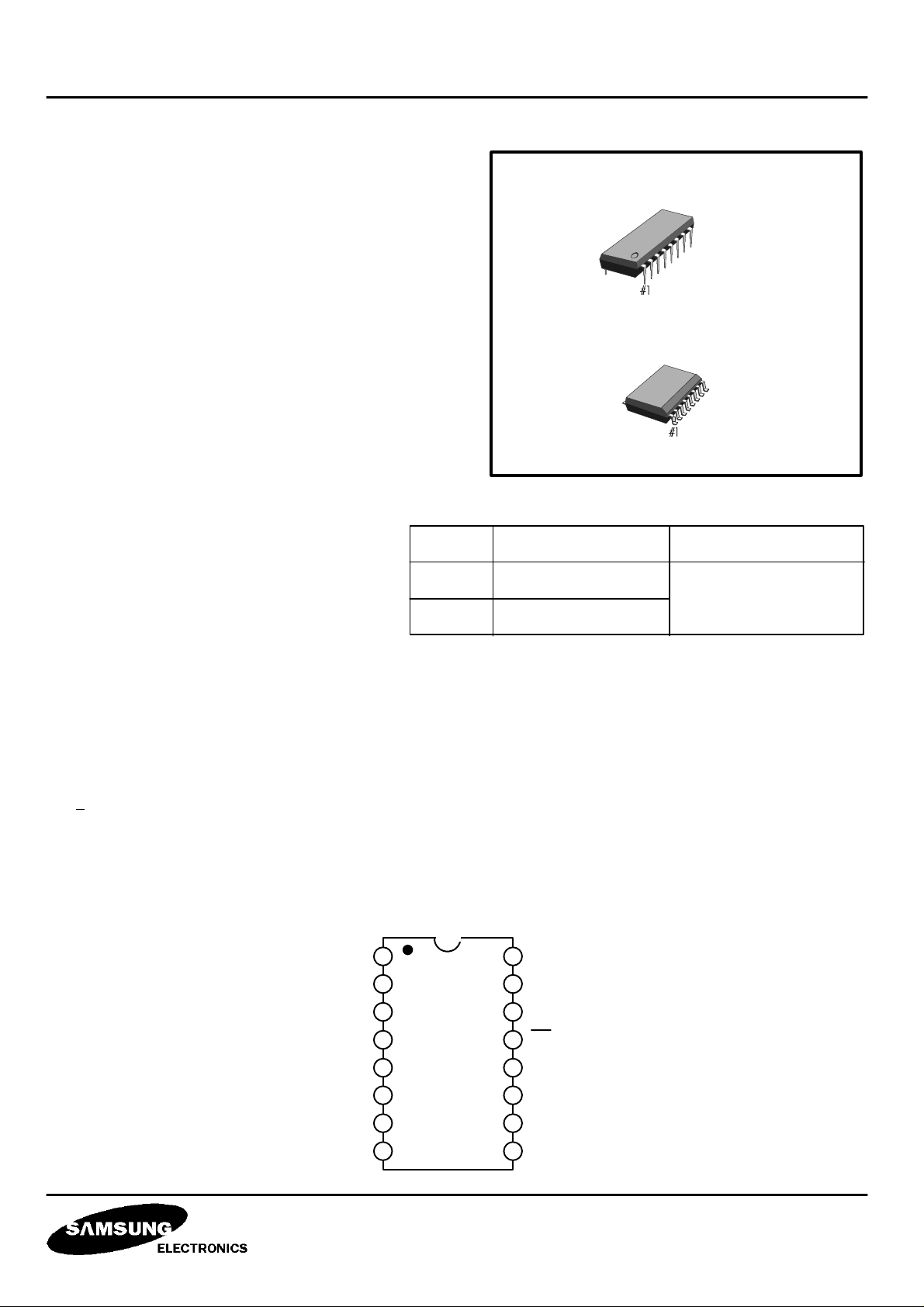
ORDERING INFORMATION
16-DIP-300
16-SOP-BD300 - SG
FEATURES
• Complete CODEC and filtering system
• Encoding / Decoding : 8 bits µ-law PCM
• On-chip auto zero, sample and hold,
and precision voltage references
• Low power dissipation : 60mW ( operating )
3mW ( standby )
• + 5V operation
• TTL or CMOS compatible
• Automatic power down
PIN CONFIGURATION
V
GNDA
BB
1
2
Device Package Operating Temperature
KS8620N
16-DIP-300
0oC ~ + 70oC
KS8620D
16-SOP- BD300 - SG
16
VFIXI+
15
VFXI-
VFRO
V
FS
D
BCLKR/CLKSEL
MCLKR/PDN
CC
3
4
5
R
6
R
7
8
KS8620
14
13
12
11
10
GS
X
TS
X
FS
X
D
X
BCLK
X
9
MCLK
X
KS8620
BLOCK DIAGRAM
R1
Analog In
15
16
R2
VFxI-
VFxI+
1 Chip CODEC for Digital Answering phone
14
GSx
+
RC Active
Filter
Switched
Capacitor
B.P.F
comparator
Auto-zero
logic
Sample & Hold
DAC
11
Dx
VFRO
Voltage
Reference
3
Power
Amplifier
RC Active
Filter
Switched
Capacitor
L.P.F
A/D
Control
Logic
Sample & Hold
DAC
Timing and Control
X’it
register
DE
Receive
register
CLK
6
13
DR
/TSx
4
Vcc
1
2
9 8
10 7
VBB
GNDA
MCLKx
MCLKR /
BCLKx
PDN
BCLKR /
CLKSEL
5
FSR
12
FSx
Fig 1. Block Diagram
KS8620
1 Chip CODEC for Digital Answering phone
PIN DESCRIPTION
Pin No Symbol Description
10
11
12
13
14
1
2
3
4
5
6
7
V
BB
GNDA
VFRO
V
CC
FS
R
D
R
BCLKR /
CLKSEL
VBB = -5V + 5%
Analog ground
Analog output of the receiver filter
Vcc = +5V + 5%
Receive frame sync pulse. 8KHz pulse train.
PCM data input
Logic input which selects either 1.536MHz / 1.544MHz or 2.048MHz for master
clock in normal operation and BCLKx is used for both TX and RX directions.
Alternately direct clock input available, vary from 64KHz to 2.048MHz.
8
MCLKR /
PDN
When MCLKR is connected continuously high, the device goes powered down .
Normally connected continuously low, MCLKx is selected for all DAC timing.
Alternately direct 1.536MHz / 1.544MHz or 2.048MHz clock input is available.
9
MCLK
BCLK
X
X
1.536MHz / 1.544MHz or 2.048MHz clock input is available
May be vary from 64KHz 2.048MHz, but BCLKx is externally tied with MCLKx
in normal operation.
D
FS
TS
GS
X
X
X
X
PCM data output.
TX frame sync pulse. 8KHz pulse train.
Changed from high to low during the encoder timeslot. Open drain output.
Analog output of the TX input amplifier.
Used to set gain through external resistor between pin 14 to pin 15.
15
16
VFXIVFXI+
Inverting input stage of the TX analog signal.
Non-inverting input stage of the TX analog signal.
ABSOLUTE MAXIMUM RATINGS ( Ta = 25 oC)
Characteristic
Positive Supply Voltage
Negative Supply Voltage
Voltage at any Analog Input or Output
Voltage at any Digital Input or Output
Operating Temperature Range
Storage Temperature Range
Lead Temperature Range ( soldering , 10 sec )
Symbol Value Unit
Vcc
VBB
V I (A)
V I (D)
Ta
TSTG
TLEAD
Vcc + 0.3 to VBB - 0.3
Vcc + 0.3 to GNDA - 0.3
+7
-7
0 to 70
-65 to +150
300
V
V
V
V
o
o
o
C
C
C
 Loading...