

Samsung KS7212 Datasheet
KS7212 TIMING & SYNC. GENERATOR FOR B/W CCD
ORDERING INFORMATION
GENERAL DESCRIPTION
The KS7212 is a CMOS integrated circuit designed for
making various timing pulses for B/W CCD camera.
FEATURES
- Compatible with both EIA and CCIR mode
(EIA : KC73125(U)-M, CCIR : KC73129(U)-M)
- Built in auto iris function (Electronic Exposure)
- Mirror mode timing generation
- Field interlace mode only
- Timing and sync one chip IC
- Oscillation frequency
EIA : 19.06992MHz, CCIR : 18.93750MHz
APPLICATION
- B/W CCD Camera
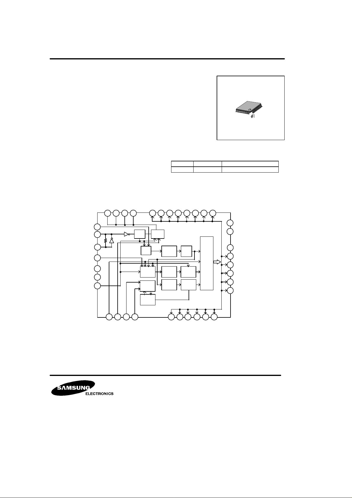
BLOCK DIAGRAM
ϕH4
ϕH3
ϕH1
ϕH2
38 37 36 35 30 29 28 27 26 25 2433
CL
43
1/2
1/606
High/Low
Control
1/525
or
1/625
Shutter
Speed
ROM
TS2
TS1
TS0
PWR
41
X2
40
X1
45
46
47
48
RG
GATE1
48-QFP-0707
Device Package Operating Temperature
KS7212 48-QFP-0707
XSUB
XV2
XV1
XSG1
Horizontal
ROM
Vertical
ROM
Shutter
Speed
Count
F/F
F/F
Shutter
Speed
Control
XV3
XSG3
GATE2
XV4
-20~75°C
22
SHP
21
SHD
CLP1
18
CLP2
17
CLP3
16
DFDO
15
CLEN
14
WIN
13
2 3 41 127 8 9 10 11
EE1
MD2
MD1
EE2
FLD
PBLK
CSYNC
CBLK
VD
HD

KS7212 TIMING & SYNC. GENERATOR FOR B/W CCD
PIN DESCRIPTIONS
No Symbol I/O Description Remark
1 MD2 I CCIR/EIA mode selection * Information (1)
2 MD1 I NORMAL/MIRROR mode selection * Information (1)
3 EE1 I EE mode control input 1 * Information (2)
4 EE2 I EE mode control input 2 * Information (2)
5 VSS1 - Ground
6 VDD1 - +5V
7 FLD O Field separation pulse
8 PBLK O Pre - blanking pulse
9 CSYNC O Composite Sync.pulse
10 CBLK O Composite Blanking pulse
11 VD O Vertical driving pulse
12 HD O Horizontal driving pulse
13 WIN O Window pulse
14 CLEN O 1/2 HD frequency pulse
15 DFDO O 1/2 VD frequency pulse
16 CLP3 O Clamp pulse 3 (Dummy black level)
17 CLP2 O Clamp pulse 2 (Optical black level)
18 CLP1 O Clamp pulse 1 (Optical black level)
19 VSS2 - Ground
20 VDD2 - +5V
21 SHD O Data Sample & Hold pulse
22 SHP O Pre - Charge Sample & Hold pulse
23 VSS3 - Ground
24 XV4 O Vertical transfer clock 4
25 XSG3 O Read out Pulse 3
26 V3 O Vertical transfer clock 3
27 XSG1 O Read out Pulse 1
28 XV1 O Vertical transfer clock 1
29 XV2 O Vertical transfer clock 2
30 XSUB O Shutter speed control for auto Iris
31 VDD3 - +5V
32 VSS4 - Ground
33
34 VDD4 - +5V
35
36
37
38
39 VSS5 - Ground
40 X1 I
41 X2 O Oscillation clock Output
42 VDD5 O +5V
43 CL O
44 VSS6 - Ground
45 TS2 I Test Input 2
46 TS1 I Test Input 1
47 TS0 I Test Input 0
48 PWR - Power On Reset
ϕRG
ϕH2
ϕH1
ϕH3
ϕH4
O Reset gate pulse
O Horizontal transfer pulse 2 ( Mirror mode)
O Horizontal transfer pulse 1 ( Normal mode’H’)
O Horizontal transfer pulse 3 ( Normal mode’H2’)
O Horizontal transfer pulse 4 ( Mirror mode )
Oscillation clock Input EIA : 19,069928MIHz
CCIR : 18.93750MHz
1/2 Oscillation clock EIA : 9.953496Mhz
CCIR : 9.46875MHz

KS7212 TIMING & SYNC. GENERATOR FOR B/W CCD
Information 1) MD2 and MD1 mode selection ( Pull - down )
MD2 MD1 MODE
L
H
Information 2 ) EE2 and EE1 shutter speed mode selection ( Pull- up )
L EIA NORMAL
H EIA MIRROR
L CCIR NORMAL
H CCIR MIRROR
EE2 EE1 MODE
L
H
L SHUTTER SPEED STOP
H SHUTTER SPEED UP
L SHUTTER SPEED DOWN
H SHUTTER SPEED STOP
ABSOLUTE MAXIMUM RATINGS
Characteristics Symbol Value Unit
Supply Voltage V
Input Voltage V
Output Voltage V
Operating Temperature T
Storage Temperature T
CC
I
O
OPR
STG
7 V
VSS-0.5 ~ VDD+0.5 V
VSS-0.5 ~ VDD+0.5 V
-20 ~ +75
-55 ~ +150
ELECTRICAL CHARACTERISTICS
(VDD=5V, Ta=25°C, unless otherwise specified)
Characteristics Symbol Test Condition Min Typ Max Unit
Supply Voltage V
Input Voltage
Output Voltage 1
Output Voltage 2 V
(CL, RG, SHP, SHD) V
Output Voltage 3 V
(H1, H2, H3, H4) V
DD
V
IH
V
IL
V
OH1
V
OL1
OH2
OL2
OH3
OL3
- 4.75 5.0 5.25 V
- 0.7V
DD
- - V
- - - 0.3V
IOH1=-2mA VDD-0.5 - - V
ICL1=4mA - - 0.4 V
ICH2=-4mA VDD-0.5 - - V
IOL2=3mA - - 0.4 V
ICH3=-8mA VDD-0.5 - - V
ICL3=8mA - - 0.4 V
°C
°C
DD
V

KS7212 TIMING & SYNC. GENERATOR FOR B/W CCD
AC CHARACTERISTICS
tr
90%
PULSES
XSG1 , XSG3
XV1 , XV2 , XV3 , XV4
H1 , H2 , H3 , H4
RG
XSUB
SHP , SHD , CLP1 ,
CLP2 , CLP3 , DFD0 ,
CLEN , WIN , HD , VD ,
CBLK , CSYNC , FLD
tf
twh
twl
twh twl tr tf
2.3
26
11
1.5
2.5
32
13
2.0
26 32
51
13
0.5
0.015
11
5
14
12
0.5
16 13
0.9VDD
0.1VDD10%
12
0.5
16
Unit
us
us
ns
ns
us
ns
Min. Typ. Max.Min. Typ. Max.Min. Typ. Max.Min. Typ. Max.
0.5
0.24
11
5
14
KS7212 TIMING & SYNC. GENERATOR FOR B/W CCD
OPERATING PRINCIPLES & METHOD
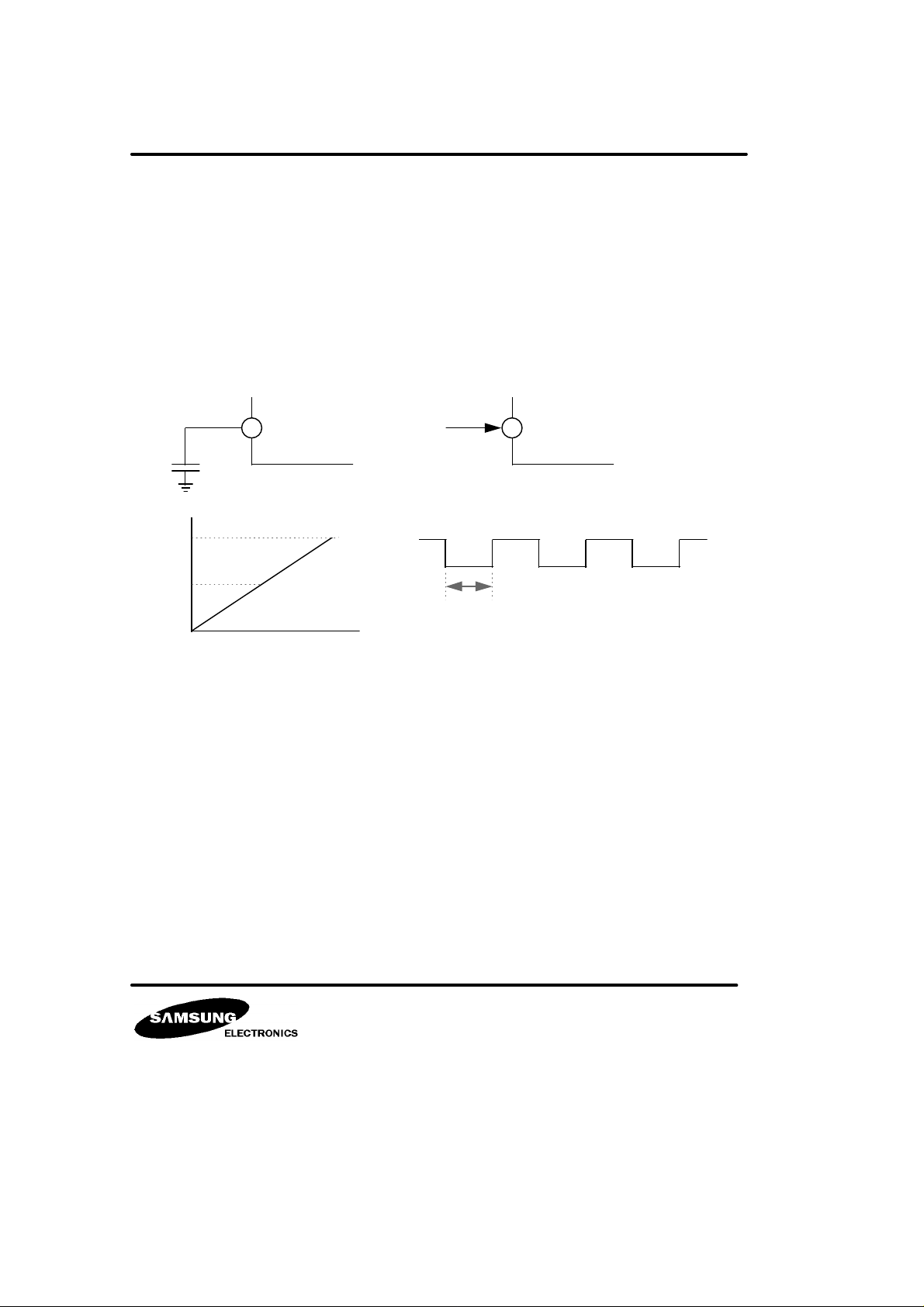
POWER ON RESET
KS7212 has two reset methods. The one is power on reset and the other is normal reset.
When user wants to use power on reset , which generates automatical reset signal that is needed to initialize the KS7212
internal system when power is on, user should be connect 1000pF capacitor at PWR ( pin 48 ) termial.
Power on reset system has internal 100Kohm pull up resister. So , user can control reset signal timing when user changes
value of capacitor , which is connected to PWR terminal.
When user wants to use normal reset , user should be remove capacitor from PWR terminal , and supplies reset signal to
PWR terminal.
KS7212
48 48
1000pF
2.4 ~
2.6 V
Fig. 1 POWER ON RESET Fig. 2 NORMAL RESET
When use u-Com system , reset signal can be supplied three times and times of 1 signal
should be larger than four times of CL clock.
RESET
SIGNAL
KS7212
840ns

KS7212 TIMING & SYNC. GENERATOR FOR B/W CCD
APPLICATION CIRCUIT ( EIA , NORMAL mode )
TO VERTICAL
TO CCD
252627282930313233343536
DRIVER
VDD
37
38
39
19.0699MHz
X-tal
VDD
* Application circuit for normal mode
EIA : 19.06992MHz
CCIR : 18.93750MHz
40
41
42
43
44
45
46
47
48
1 2 3 4 5 6 7 8 9 10 11 12
KS7212
TIMING & SYNC GEN
24
23
22
21
20
19
18
17
16
15
14
13
TO SIGNAL
PROCESSOR
 Loading...