

Page 1
Samsung Electronics 7-1
Schematic Diagram
This Document can not be used without Samsung’s authorization.
7. Schematic Diagram
7-1 Overall Block Diagram ..................................................................................... 7-2
7-2 FRONT ............................................................................................................... 7-3
7-3 BLUETOOTH ..................................................................................................... 7-4
7-4 AMP ................................................................................................................... 7-5
7-5 MAIN .................................................................................................................. 7-6
7-6 MICOM ............................................................................................................... 7-7
7-7 ANALOG ........................................................................................................... 7-8
7-8 HDMI .................................................................................................................. 7-9
7-9 SMPS ................................................................................................................. 7-10
Page 2
7-2 Samsung Electronics
Schematic Diagram
This Document can not be used without Samsung’s authorization.
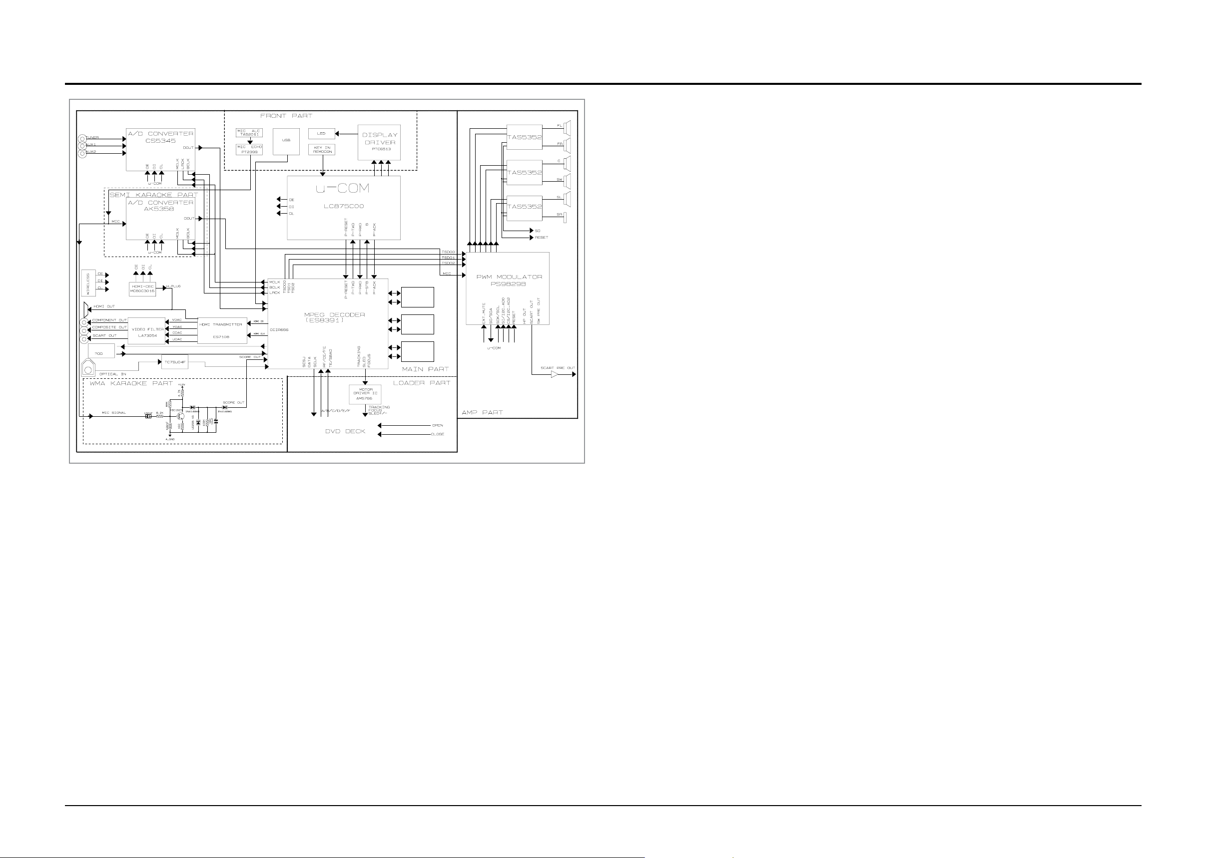
7-1 Overall Block Diagram
DRAM
M12L12816B
FLASH
AT26DF161A
ROM
24C08A
The main system uses the MPEG (ES8391). The HDMI Tx IC is ES7108S. The main system consists of major circuit
blocks such as HDMI, POWER, CEC, FRONT, KARAOKE, etc.
The Main system includes the functional blocks such as FM-TUNER, AUX INPUT, ADC, Sub_Micom, etc.
The information about the main system operation is displayed on the VFD of Front Board.
Audio signal is transmitted through Analog 2V between the main body and the speaker, and is input to the AMP through
ADC (CS5345).
First, MPEG (ES8391) receives RF signal from the PICK_UP and decodes Video and audio signal.
HDMI IC is implemented by the I2C. The Micom and MPEG control each other through RXD and TXD communication.
The Power supplies voltages for each component using the SMPS. The Power can be switched turned on or off through
the Micom port. The functions and DPL2 function can be controlled by the front keypad and remote control.
Page 3
Samsung Electronics 7-3
Schematic Diagram
This Document can not be used without Samsung’s authorization.
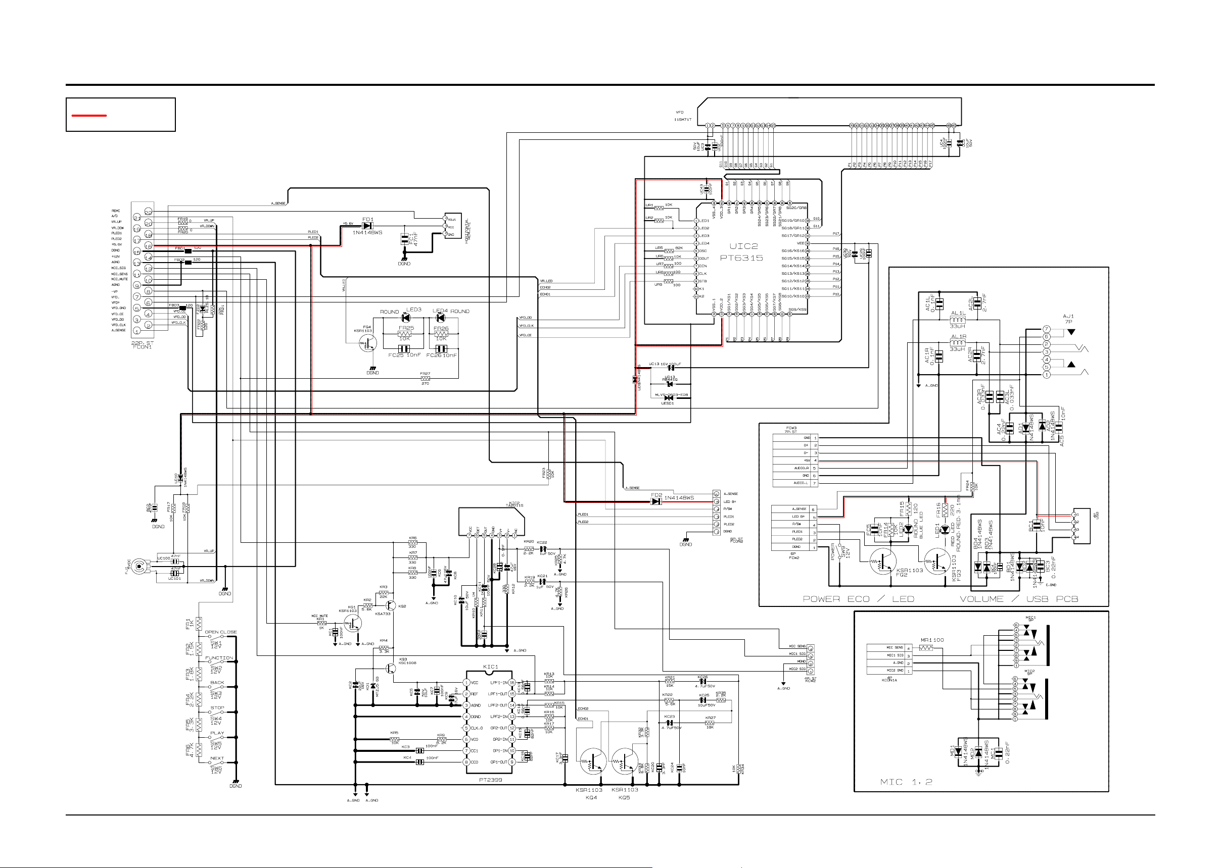
7-2 FRONT
POWER
Page 4

7-4 Samsung Electronics
Schematic Diagram
This Document can not be used without Samsung’s authorization.
7-3 BLUETOOTH
POWER
Page 5

Samsung Electronics 7-5
Schematic Diagram
This Document can not be used without Samsung’s authorization.
7-4 AMP
TP6
TP7
TP8
TP6
TP7
TP8
TP7
TP7
Page 6

7-6 Samsung Electronics
Schematic Diagram
This Document can not be used without Samsung’s authorization.
7-5 MAIN
POWER
AUDIO
VIDEO
TP2
TP9
TP10
TP11
TP12
TP13
TP2
TP13
TP12
TP11
TP10
TP9
TP15
TP16
TP15
TP16
Page 7

Samsung Electronics 7-7
Schematic Diagram
This Document can not be used without Samsung’s authorization.
7-6 MICOM
POWER
TP2
TP3
TP4
TP5
TP3
TP2
TP4 TP5
Page 8

7-8 Samsung Electronics
Schematic Diagram
This Document can not be used without Samsung’s authorization.
7-7 ANALOG
TP1
TP9
TP2
TP3
TP4
TP5
POWER
AUDIO
VIDEO
TP1
TP3
TP2
TP1
TP4TP5
TP9
TP10
TP11
TP10
TP11 TP12
TP12
Page 9

Samsung Electronics 7-9
Schematic Diagram
This Document can not be used without Samsung’s authorization.
7-8 HDMI
IC31
ES7108S
TP13
TP14
POWER
AUDIO
VIDEO
HDMI OUT
TP14
TP13
Page 10

7-10 Samsung Electronics
Schematic Diagram
This Document can not be used without Samsung’s authorization.
7-9 SMPS
1T 6
16-PTR
O
7
004
FU
1SD
F
u7
.
4
/V0
01
1
S
C
3SDZ
4BD
M 301
2
S
C
8
A8
22CA
M
2
S
U
2
T
6
1
6
-PTR
O
Hu51
17
L
3SR
K
7
4
W
2
5
S
R
07
4
0
01 W
2
6
S
R
Hu
9
.
2
19L
V
8
+
DNG
V5+
V5+
V3
.3+
V3
.3
+
DN
G
D
NG
S
/
P
NO/
P
V
6
.5+
DNG
V3.4
+ DF
V
V3.4-
DFV
PV-
1
S
R
K033W1
V03
2 B4-
U
1
A
S
3
0
1
/
V
0
3
6
3
S
C
B
0574
N
1
1SDZ
2SR
K9.
3
2SD
Z
B0574
N
1
4SR
K
22
 Loading...