

GSM TELEPHONE
GT-S5570
GSM TELEPHONE
CONTENTS
Safety Precautions
1.
Specification
2.
Product Function
3.
Exploded View and Parts list
4.
MAIN Electrical Parts List
5.
Level1Repair
6.
Level2Repair
7.
Level3Repair
8.
Reference data
9.
Notice
All functionality, features, specifications and other
product information provided in this document inclu
ding, but not limited to, the benefits, design, pricing,
components, performance, availability, and capabiliti
es of the product are subject to change without
-
notice or obligation. Samsung reserves the right to
make changes to this document and the product
described herein, at anytime, without obligation on
Samsung to provide notification of such change.
:

This Service Manual isaproperty of Samsung Electronics Co.,Ltd.
Any unauthorized use of Manual can be punished under applicable
International and/or domestic law.
Samsung Electronics Co.,Ltd.
ⓒ
2010. 12.
Rev.1.0

Specification
2.
GSM General Specification
2-1.
GSM850
Phase 1
Freq.
Band[MHz]
Uplink/Downlin
k
ARFCN range 128~251
Tx/Rx spacing 45MHz 45MHz 95MHz 80MHz 190MHz 45MHz
Mod. Bit rate/
Bit Period
Time Slot
Period/Frame
Period
824~849
869~894
270.833kbp
s
3.692us
576.9us
4.615ms
EGSM 900
Phase 2
880~915
925~960
0~124 &
975~1023
270.833kbp
s
3.692us
576.9us
4.615ms
DCS1800
Phase 1
1710~1785
1805~1880
512~885 512~810
270.833kbp
s
3.692us
576.9us
4.615ms
PCS1900
1850~1910
1930~1990
270.833kbp
s
3.692us
576.9us
4.615ms
WCDMA210
0
1922~1977
2112~2167
UL:9612~98
88DL:10562
~10838
3.84Mcps 3.84Mcps
FrameLengt
h:
10ms
Slotlength:
0.667ms
WCDMA900
880~915
925~960
UL:2712~28
63,DL:2937
~3088
FrameLengt
h:
10ms
Slotlength:
0.667ms
Modulation 0.3GMSK 0.3GMSK 0.3GMSK 0.3GMSK
MS Power
Power Class
Sensitivity -102dBm -102dBm -100dBm -100dBm -106.7dBm -106.7dBm
TDMA Mux 8 8 8 8
Cell Radius 35Km 35Km 2Km 2Km 2Km 2Km
33dBm~5dBm33dBm~5dBm30dBm~0dBm30dBm~0dBm24dBm~-
5pcl ~
19pcl
pcl
5
~19
pcl0pcl
~15
2-1
pcl
pcl
0
~15
QPSKHQPSKQPSKHQPS
24dBm~-
pcl
50dBm
max+24dB
3(
m)
8
50dBm
max+24dB
3(
K
m)
8
Specification
GSM Tx Power Class
2-2.
TX Power
control
GSM850
level
533±2
631±2
729±2
827±2
925±2
10 23±2
11 21±2
12 19±2
dBm
dBm
dBm
dBm
dBm
dBm
dBm
dBm
TX Power
control
EGSM900
level
533±2
631±2
729±2
827±2
925±2
10 23±2
11 21±2
12 19±2
dBm
dBm
dBm
dBm
dBm
dBm
dBm
dBm
TX Power
control
DCS1800
level
030±3
128±3
226±3
324±3
422±3
520±3
618±3
716±3
dBm
dBm
dBm
dBm
dBm
dBm
dBm
dBm
TX Power
control
PCS1900
level
030±3
128±3
226±3
324±3
422±3
520±3
618±3
716±3
dBm
dBm
dBm
dBm
dBm
dBm
dBm
dBm
13 17±2
14 15±2
15 13±2
16 11±3
17 9±3
18 7±3
19 5±3
dBm
dBm
dBm
dBm
dBm
dBm
dBm
13 17±2
14 15±2
15 13±2
16 11±3
17 9±3
18 7±3
19 5±3
dBm
dBm
dBm
dBm
dBm
dBm
dBm
2-2
814±3
912±4
10 10±4
11 8±4
12 6±4
13 4±4
14 2±5
15 0±5
dBm
dBm
dBm
dBm
dBm
dBm
dBm
dBm
814±3
912±4
10 10±4
11 8±4
12 6±4
13 4±4
14 2±5
15 0±5
dBm
dBm
dBm
dBm
dBm
dBm
dBm
dBm

Operation Instruction and Installation
3.
Main Function
GSM(2G EDGE/GPRS)
•
•
HSDPA
•
3.14”
Music player, Voice Recorder
•
•
A-GPS/BT v3.0/USB v2.0/WiFi
•3M
•
•
•
•
•
Camera
FM Radio Receiver
Bluetooth v3.0
USB
Sensors: Accelerometer, Compass
TouchWiz
Mbps
7.2
QVGA TFT Full Touch(c-type
FS/Wi-Fi
2.0
Light for Android(Multiple SNS(Facebook, Myspace, Twitter)
3.0
Multiple IM(Parling: AOL, G-talk))
850/900/1800/1900
)
(802.11
802.11n /
GPS
b/n/g)
Touch WIZ
•
SMS/MMS/Email
•
UI,Application store
3.0
3-1
SAMSUNG Proprietary-Contents may change without notice
This Document can not be used without Samsung's authorization
Level
6.
Software Download
6-1.
1
Repair
6-1-1.
ㆍ
ㆍ
ㆍ
ㆍ
ㆍ
ㆍ
ㆍ
ㆍ
-
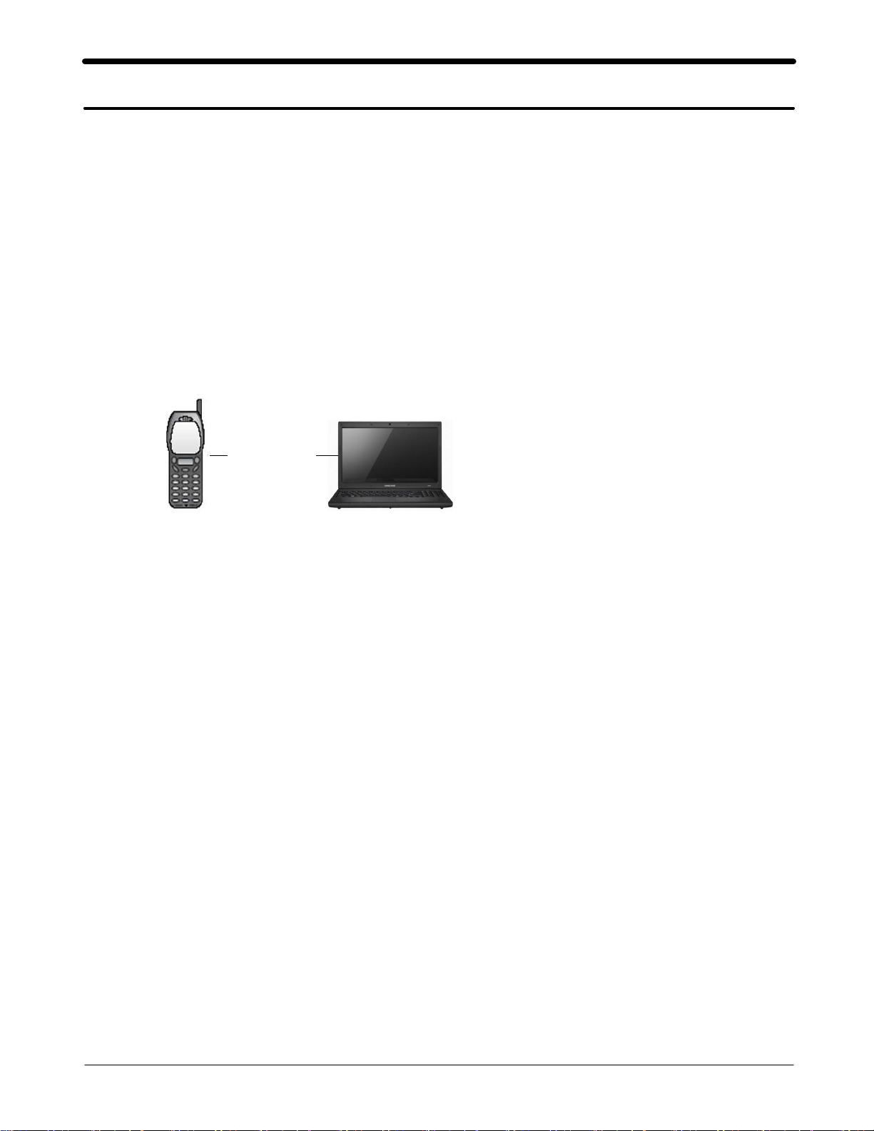
Pre-requisite for Download
Downloader Program
GT-S5570 Mobile Phone
Data Cable
JIG BOX(GH99-36900A)
RF Test Cable(GH39-00985A)
JIG Cable(GH39-01160A)
Adapter(GH99-38251A)
Binary files
Diagram of Connection:
Mobile Phone(with Battery)
(
Odin Multi Downloader v4.
Data Cable
PC
38
)
6-1
SAMSUNG Proprietary-Contents may change without notice
This Document can not be used without Samsung's authorization
Level1Repair
6-1-2.
S/W Download Process
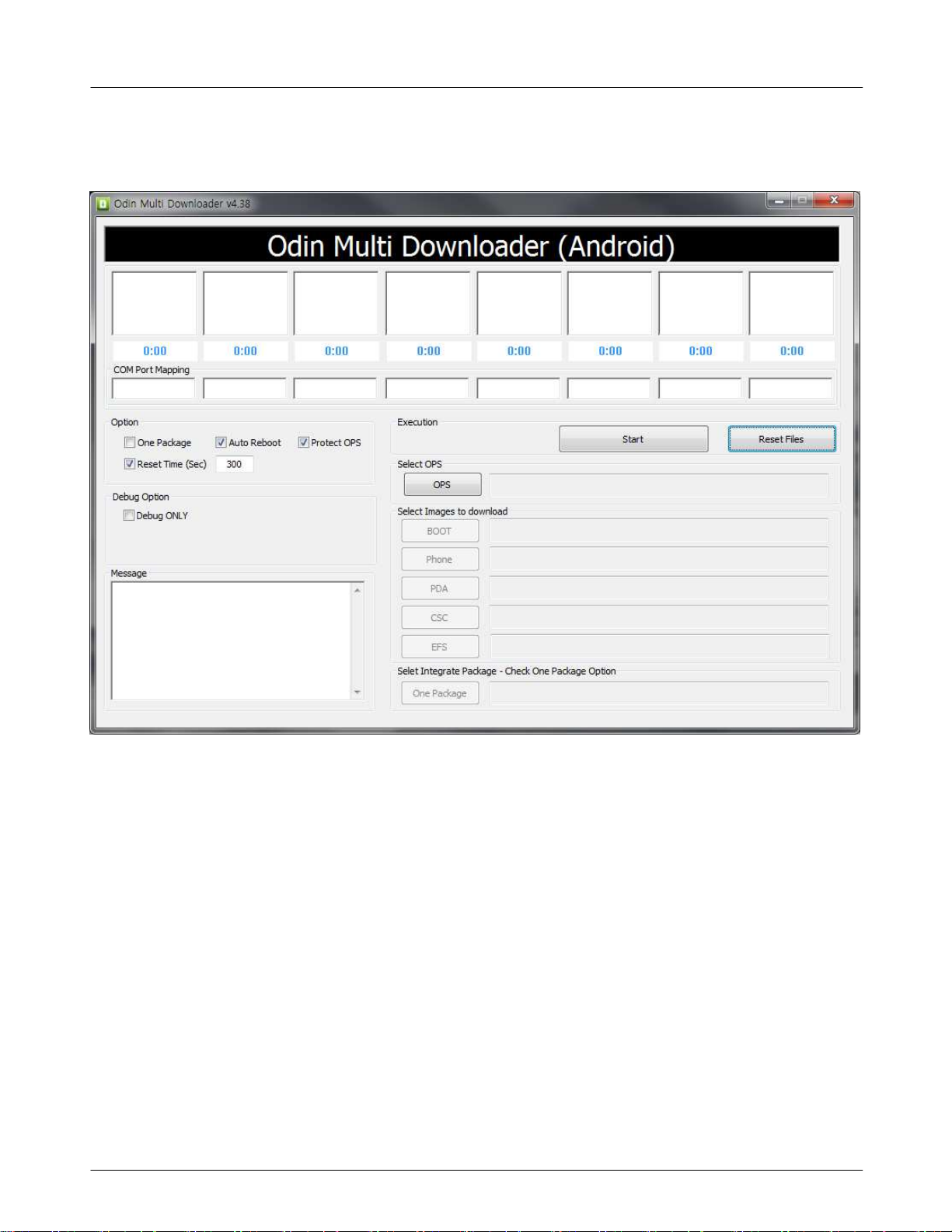
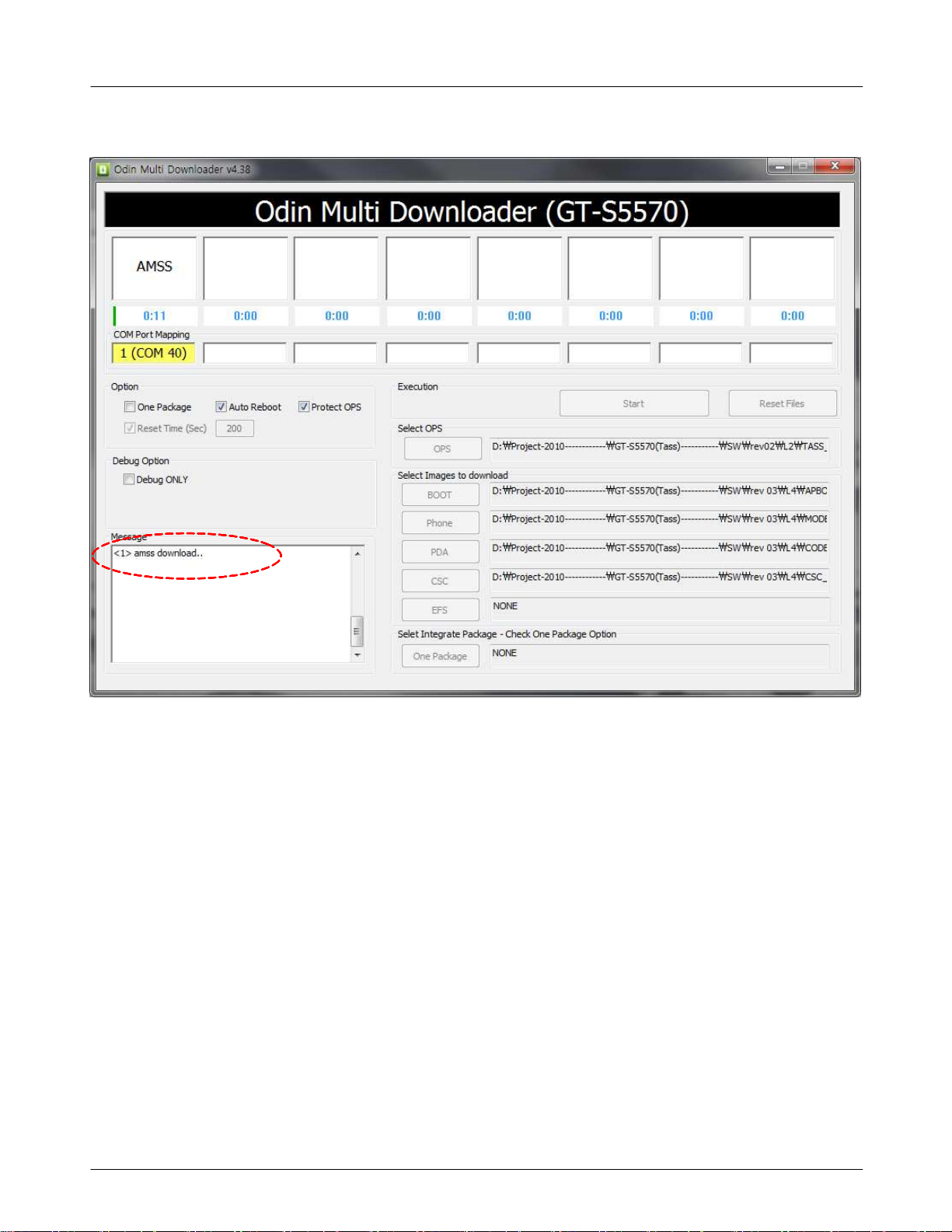
Load the binary download program by executing the
1.
"
Odin Multi Downloader v4.
38
"
6-2
SAMSUNG Proprietary-Contents may change without notice
This Document can not be used without Samsung's authorization
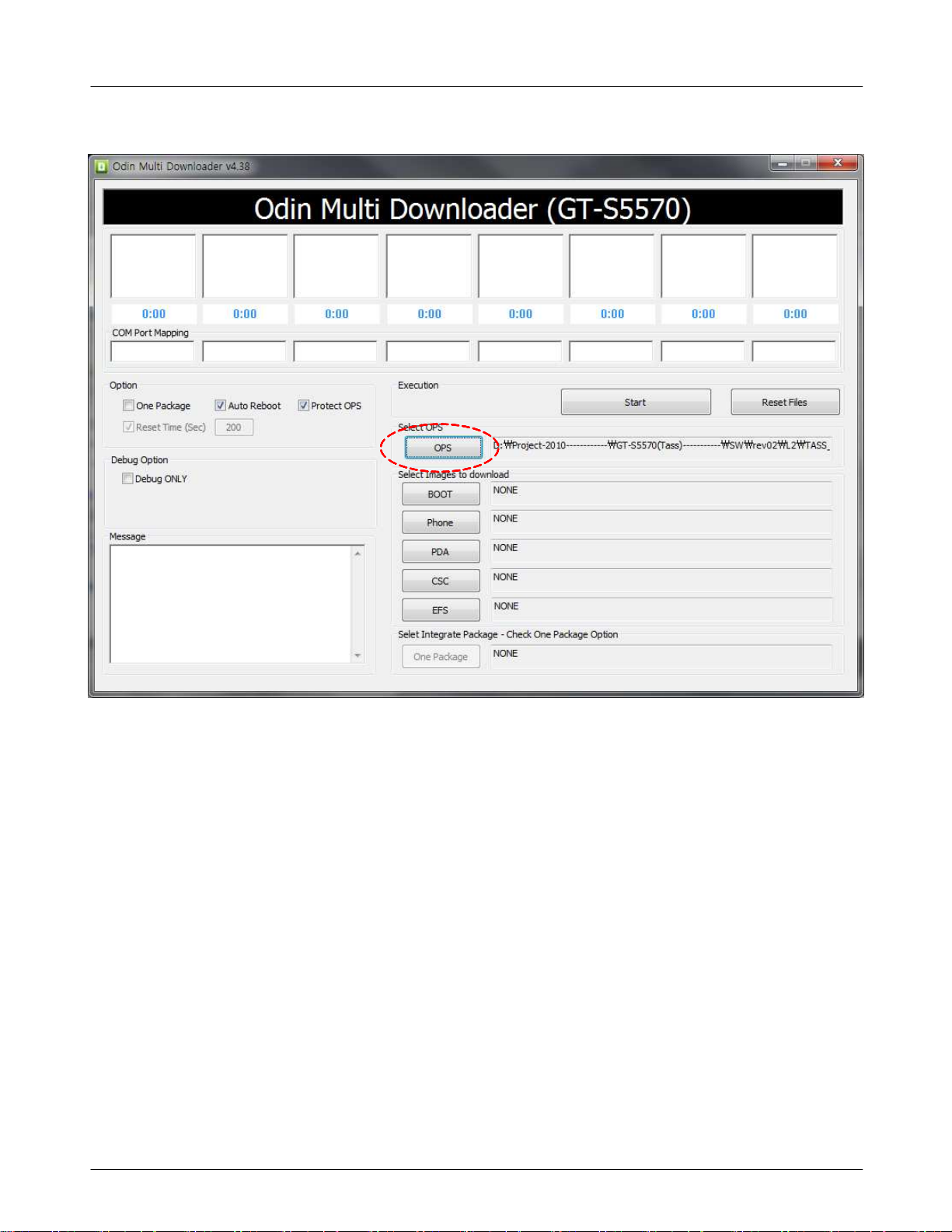
Select OPS file(TASS_v1.0.ops) from the folder that you saved the binary files.
2.
Level1Repair
6-3
SAMSUNG Proprietary-Contents may change without notice
This Document can not be used without Samsung's authorization
Level1Repair
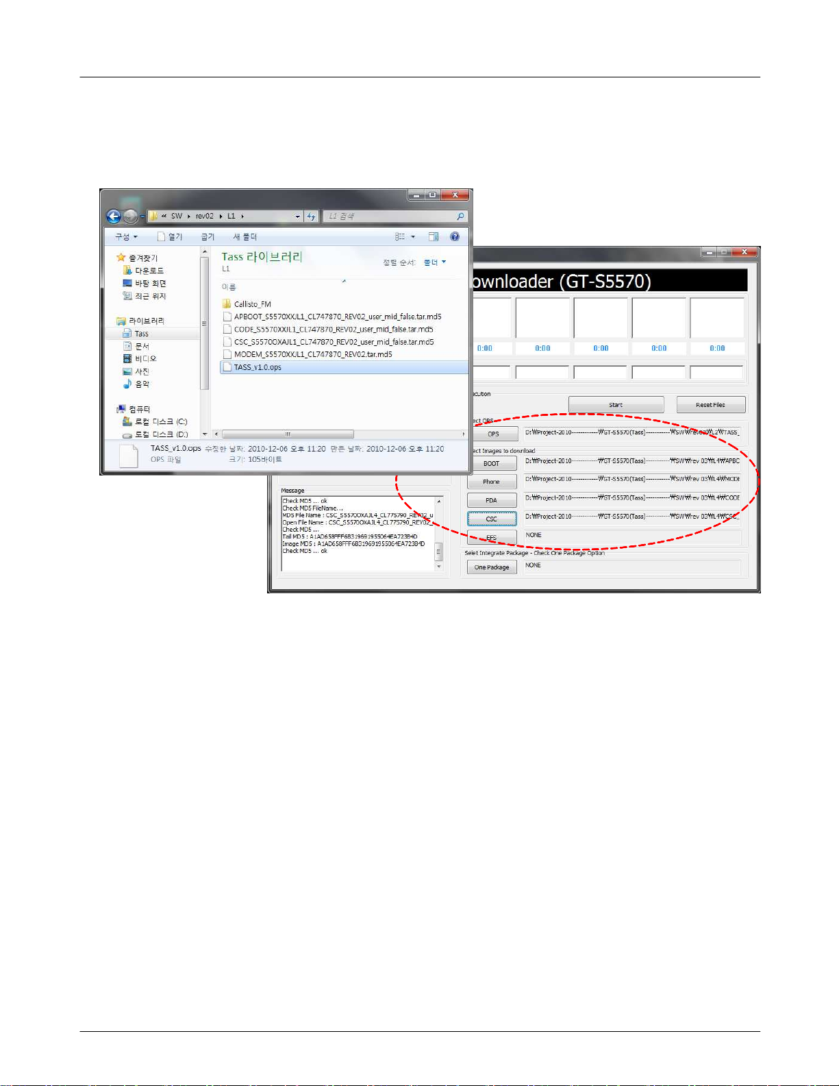
Load the file of Bootloader, Amss, PDA, CSC files from the folder that you saved the binary
4.
files.
6-4
SAMSUNG Proprietary-Contents may change without notice
This Document can not be used without Samsung's authorization
Level1Repair
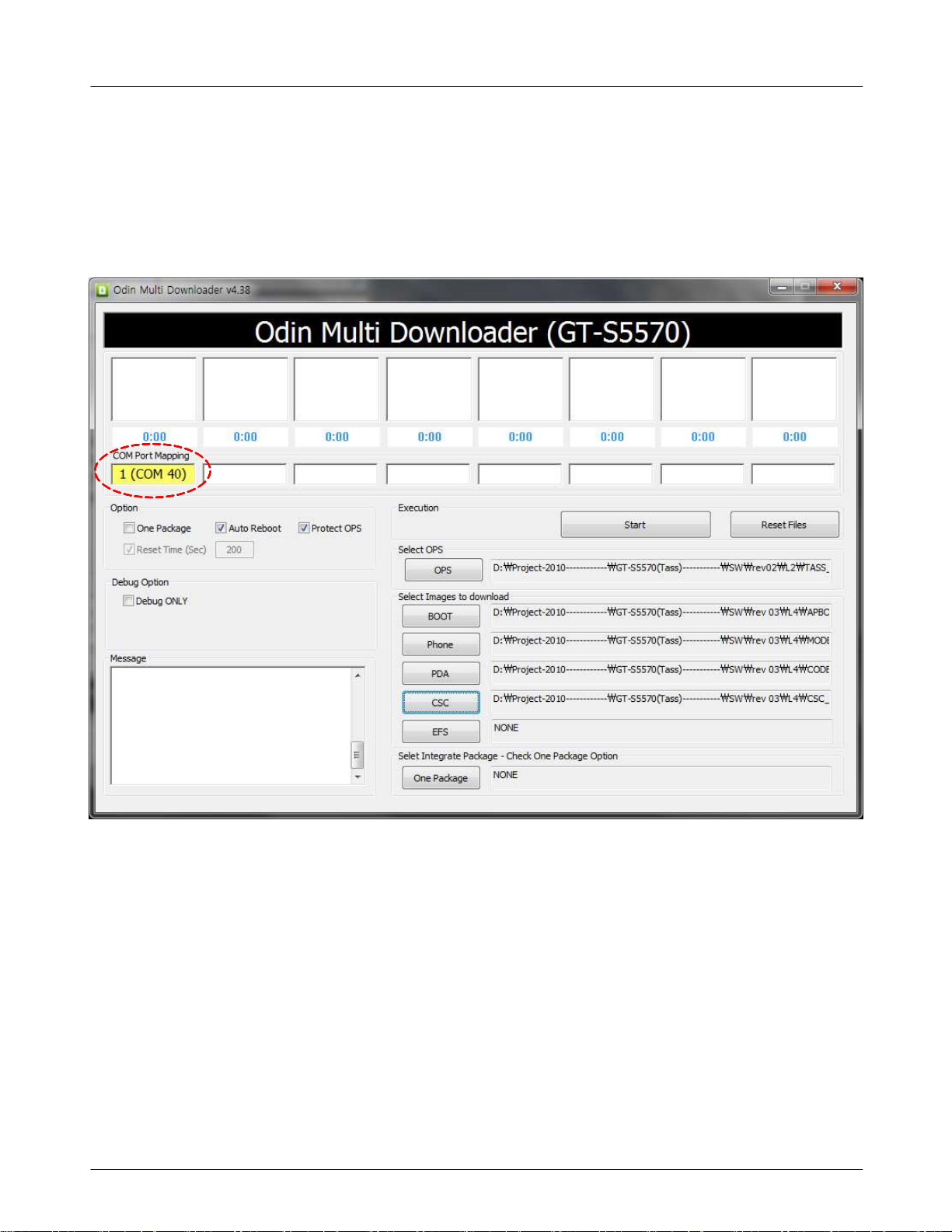
COM Port Mapping change to
5.
yellow
colour when the phone with download mode is
connected to PC by data cable.
cf. You have to set the phone asadownload mode by pressing Volume down
Key(Home Key)+Power key simultaneously before connecting to PC
.
Then, the port would be searched.
Middle
+
6-5
SAMSUNG Proprietary-Contents may change without notice
This Document can not be used without Samsung's authorization
Level1Repair
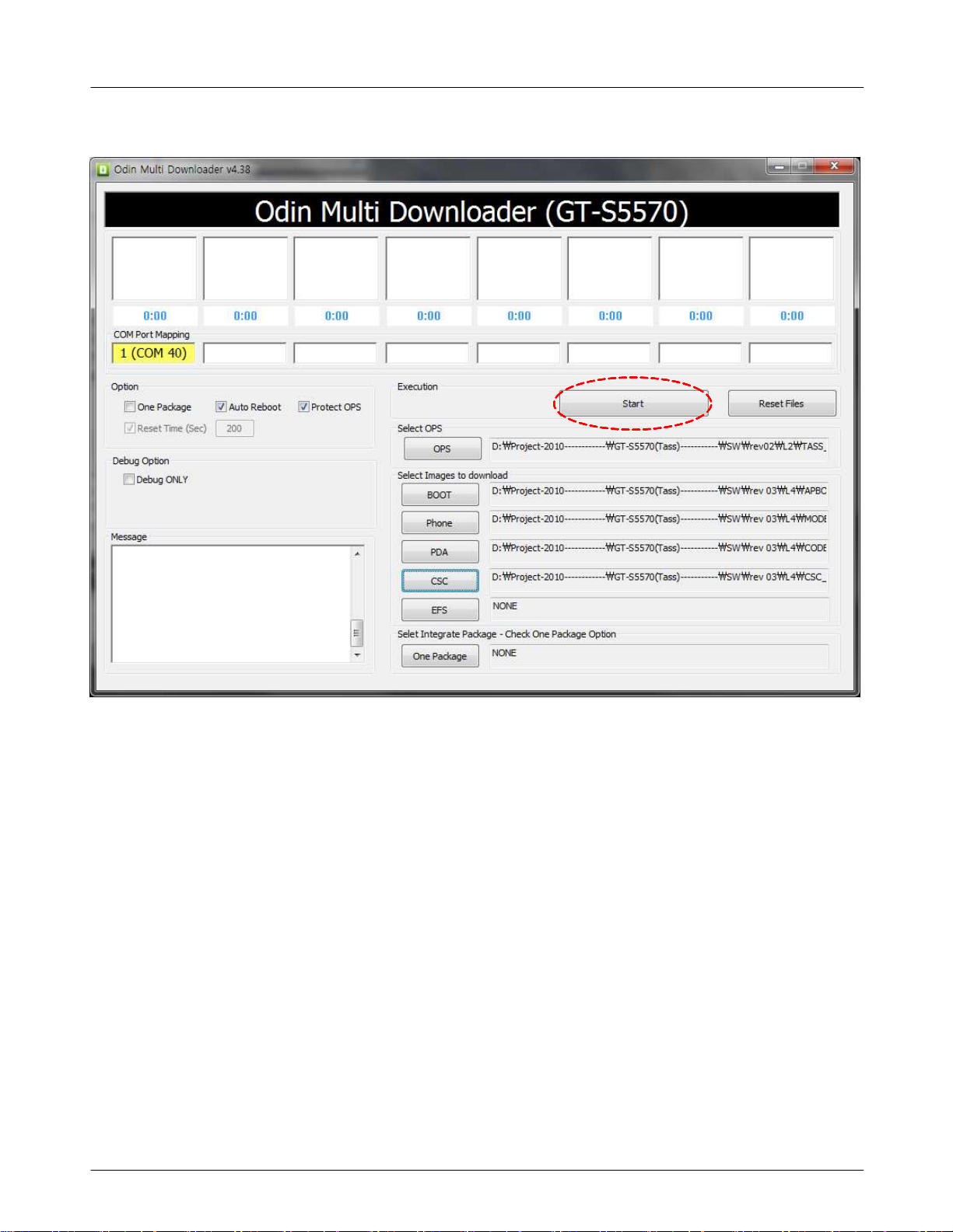
Click the
5.
Start
buttonwhen the Port searched.
6-6
SAMSUNG Proprietary-Contents may change without notice
This Document can not be used without Samsung's authorization
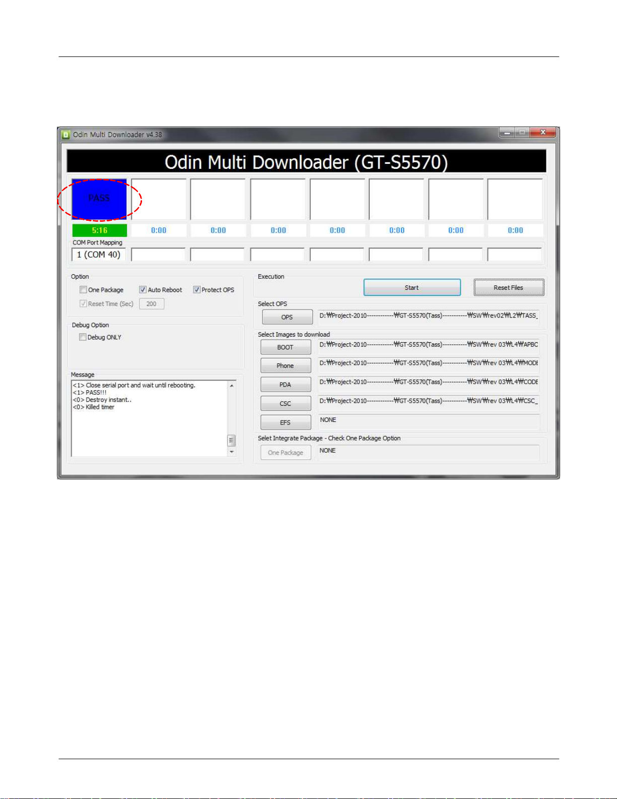
It will start to download.
Level1Repair
6-7
SAMSUNG Proprietary-Contents may change without notice
This Document can not be used without Samsung's authorization
Level1Repair
When downloading is finished successfully, there is
6.
a"
PASS
message.
"
Confirm the downloaded version name and etc.
7.
*#1234#
SAMSUNG Proprietary-Contents may change without notice
This Document can not be used without Samsung's authorization
:
6-8

Reference Abbreviate
9.
Reference Abbreviate
Advanced Audio Coding.
AAC:
―
―
―
―
―
―
―
―
―
―
―
―
―
―
―
―
―
―
―
AVC :
BER :
BPSK:
CA :
CDM :
C/I :
DMB :
EN
ES
ETSI:
MPEG:
PN :
PS :
QPSK:
RS :
SI :
TDM :
TS
Advanced Video Coding.
Bit Error Rate
Binary Phase Shift Keying
Conditional Access
Code Division Multiplexing
Carrier to Interference
Digital Multimedia Broadcasting
European Standard
:
Elementary Stream
:
European Telecommunications Standards Institute
Moving Picture Experts Group
Pseudo-random Noise
Pilot Symbol
Quadrature Phase Shift Keying
Reed-Solomon
Service Information
Time Division Multiplexing
Transport Stream
:
9-1
SAMSUNG Proprietary-Contents may change without notice
This Document can not be used without Samsung's authorization

Safety Precautions
1.
Repair Precaution
1-1.
Repair in Shield Box, during detailed tuning. Take specially care of tuning or test, because
―
specipicty of cellular phone is sensitive for surrounding interference(RF noise).
Be careful to useakind of magnetic object or tool, because performance of parts is damaged by
―
the influence of magnetic force.
Surely useastandard screwdriver when you disassemble this product, otherwise screw will be
―
worn away.
Useathicken twisted wire when you measure level.
―
thicken twisted wire has low resistance, therefore error of measurement is few.
A
Repair after separate Test Pack and Set because for short danger(for example an overcurrent
―
and furious flames of parts etc) when you repair board in condition of connecting Test Pack and
tuning on.
Take specially care of soldering, because Land of PCB is small and weak in heat.
―
Surely tune on/off while using AC power plug, becausearepair of battery charger is dangerous
―
when tuning ON/OFF PBA and Connector after disassembling charger.
Don't use as you pleases after change other material than replacement registered on SEC System.
―
Otherwise engineer in charge isn't charged with problem that you don't keep this rules.
1-1
SAMSUNG Proprietary-Contents may change without notice
This Document can not be used without Samsung's authorization

Safety Precautions
ESD(Electrostatically Sensitive Devices) Precaution
1-2.
Several semiconductor may be damaged easily by static electricity. Such parts are called by ESD
Electrostatically Sensitive Devices), for example IC,BGA chip etc. Read Precaution below.
(
You can prevent from ESD damage by static electricity.
Remove static electricity remained your body before you touch semiconductor or parts with
―
semiconductor. There are ways that you touch an earthed place or wear static electricity prevention
string on wrist.
Use earthed soldering steel when you connect or disconnect ESD.
―
Use soldering removing tool to break static electricity.,otherwise ESD will be damaged by static
―
electricity.
Don't unpack until you set up ESD on product. Because most of ESD are packed by box and
―
aluminum plate to have conductive power,they are prevented from static electricity.
You must maintain electric contact between ESD and place due to be set up until ESD is
―
connected completely to the proper place oracircuit board.
1-2
SAMSUNG Proprietary-Contents may change without notice
This Document can not be used without Samsung's authorization
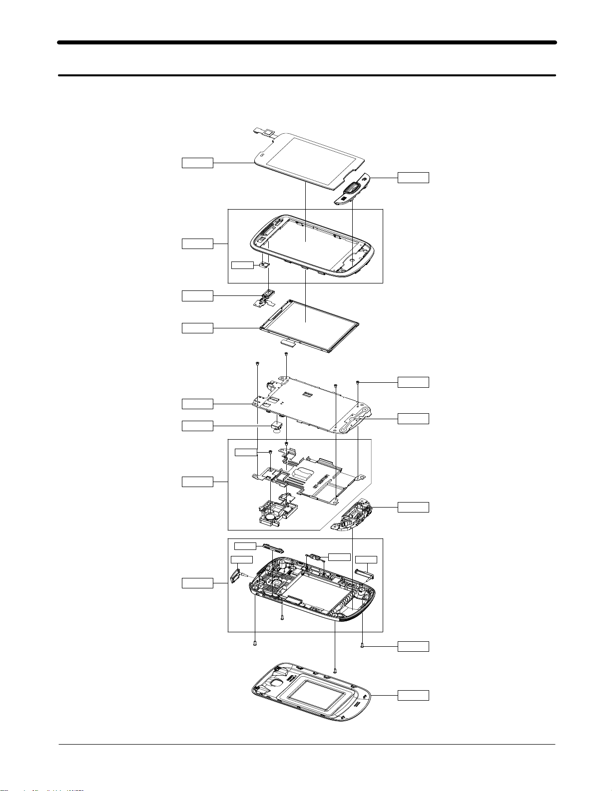
Exploded View and Parts List
4.
Cellular phone Exploded View
4-1.
QME03
QFR01
QMI03
QAR01
QLC01
QKP01
QMP01
QCA01
QMO01
QRE01
QCR92
QVO01
QRF03 QSD01
QCK02
QCR92
QME01
QSP01
QCR67
QBC00
4-1
SAMSUNG Proprietary-Contents may change without notice
This Document can not be used without Samsung's authorization

Exploded View and Parts List
Cellular phone Parts list
4-2.
Design LOC Description SEC CODE
QCR67 SCREW-MACHINE
QCR92 SCREW-MACHINE
QCA01 CAMERA MODULE-GT-S5330
3M
6001-002083
6001-002261
GH59-09906A
QAR01 ASSY ETC-RCV+SENSOR FPCB(GT_S5570) GH59-10625A
QME01 DOME SHEET-GT_S5570 GH59-10628A
QME03 TOUCH/PANEL-GT_S5570(EU/BLACK) GH59-10651A
QSP01 MODULE-SPK+INT GH59-10663A
QMP01 A/S ASSY-PBA MAIN(COMM) GH82-05484A
QLC01 ELA MODULE-LCD(GT_S5570) GH96-05032A
QKP01 ASSY KEYPAD-GT-S5570 GH98-19187A
QBC00 ASSY COVER-BATT GH98-19190A
QMO01 MODULE-MOT+BRACKET+SHIELD CAN(GT_S557 GH59-10768A
QCR92 SCREW-MACHINE
6001-002261
QFR01 ASSY CASE-FRONT GH98-19183A
QMI03 ASSY RUBBER-MIC UP GH98-19272A
QRE01 ASSY CASE-REAR GH98-19189A
QVO01 PMO COVER-VOL_KEY GH72-62658A
QCK02 PMO COVER-POWER_KEY GH72-62659A
QSD01 PMO COVER-SD GH72-62660A
QRF03 PMO COVER-USB GH72-62661A
4-2
SAMSUNG Proprietary-Contents may change without notice
This Document can not be used without Samsung's authorization

MAIN Electrical Parts List (2010.12.22)
5.
Design LOC SEC CODE Description
D600
U637
ZD501
ZD502
D400,D500
Q601
Q600
U619
U301
U303
U609
U500,U635
UME300
PAM102
PAM101
U200
PAM100
U508
U503
U501
U615
U101
UCP300
U202
U201
C522
U509
TH300
U614,V500,V503,V504
V505,V600,V601,V602
VR500,VR501,VR502
R116,R325,R509
R100,R322,R326,R500
R506,R527,R606
R4112,U628
R119
0403-001870
0404-001646
0406-001286
0406-001329
0407-001002
0504-001138
0505-001325
0505-002341
0801-003265
0801-003383
1001-001645
1001-001655
1108-000411
1201-002967
1201-003088
1201-003168
1201-003210
1202-001068
1203-006331
1203-006346
1203-006732
1205-003297
1205-004035
1205-004076
1205-004113
1209-002023
1209-002030
1404-001221
1405-001298
1405-001298
1405-001298
2007-000137
2007-000138
2007-000138
2007-000140
2007-000141
DIODE-ZENER
DIODE-SCHOTTKY
DIODE-TVS
DIODE-TVS
DIODE-ARRAY
TR-DIGITAL
FET-SILICON
FET-SILICON
IC
IC
IC
IC
MEMORY
IC
IC
IC
IC
IC
IC
IC
IC
IC
IC
IC
IC
IC
IC
THERMISTOR
VARISTOR
VARISTOR
VARISTOR
R-CHIP
R-CHIP
H
IP
R-C
R-CHIP
R-CHIP
5-1
SAMSUNG Proprietary-Contents may change without notice
This Document can not be used without Samsung's authorization

Main Electrical Parts List
Design LOC SEC CODE Description
R400
R501,R526,R600,R607
R615
R605
R616,R617
U617
R608,R609,R610,R611
R612
R300,R318,R324,R327
R409,R505,U638
R516,U616
R614,U618
R502
U639
R329,R404,R405
R109,R401
R521
R613
R507
U630
R603,R604
U629
R406
R204
R309,R313
R110
R402
R408
R407
R410
R105
R106,R107
R302,R319,R321,R335
R301
R111,R303
R308
2007-000144
2007-000148
2007-000148
2007-000149
2007-000151
2007-000153
2007-000157
2007-000157
2007-000162
2007-000162
2007-000165
2007-000168
2007-000170
2007-000172
2007-001292
2007-001298
2007-001333
2007-001339
2007-002796
2007-003004
2007-003015
2007-003030
2007-007107
2007-007132
2007-007139
2007-007309
2007-007334
2007-007468
2007-007480
2007-007573
2007-008044
2007-008045
2007-008055
2007-008298
2007-008419
2007-008516
R-CHIP
R-CHIP
R-CHIP
R-CHIP
R-CHIP
R-CHIP
R-CHIP
R-CHIP
R-CHIP
R-CHIP
R-CHIP
R-CHIP
R-CHIP
R-CHIP
R-CHIP
R-CHIP
R-CHIP
R-CHIP
R-CHIP
R-CHIP
R-CHIP
R-CHIP
R-CHIP
R-CHIP
R-CHIP
R-CHIP
R-CHIP
R-CHIP
R-CHIP
R-CHIP
R-CHIP
R-CHIP
R-CHIP
HIP
R-C
R-CHIP
R-CHIP
5-2
SAMSUNG Proprietary-Contents may change without notice
This Document can not be used without Samsung's authorization

Design LOC SEC CODE Description
R121
R332
R304,R305,R306,R307
R314,R315,R316,R317
R323
R120
R330
R403
R205
C109,C127,C154,C215
C434,L111
C103,C110,C205
C200,C204,C214,C230
C511
R200
C237
L116
C530
C101,C104,C114,C218
C519,C520
C328
C432,C433
C427
C322,L119
C102,C105,C203,C206
C210,C220,C221,C324
C506,C516,C517,C606
R104
C235
C329,C428
C406,C407
C108
C224,C226,C227,C229
C232,C233,C243,C305
C318,C524,C527,C603
U302
2007-008531
2007-008564
2007-008588
2007-008588
2007-008766
2007-008774
2007-008806
2007-008812
2007-009794
2203-000233
2203-000233
2203-000254
2203-000278
2203-000278
2203-000311
2203-000330
2203-000386
2203-000425
2203-000438
2203-000438
2203-000489
2203-000550
2203-000585
2203-000696
2203-000812
2203-000812
2203-000812
2203-000812
2203-000940
2203-000995
2203-001405
2203-002668
2203-002709
2203-002709
2203-002709
2203-002709
R-CHIP
R-CHIP
R-CHIP
R-CHIP
R-CHIP
R-CHIP
R-CHIP
R-CHIP
R-CHIP
C-CERAMIC,CHIP
C-CERAMIC,CHIP
C-CERAMIC,CHIP
C-CERAMIC,CHIP
C-CERAMIC,CHIP
C-CERAMIC,CHIP
C-CERAMIC,CHIP
C-CERAMIC,CHIP
C-CERAMIC,CHIP
C-CERAMIC,CHIP
C-CERAMIC,CHIP
C-CERAMIC,CHIP
C-CERAMIC,CHIP
C-CERAMIC,CHIP
C-CERAMIC,CHIP
C-CERAMIC,CHIP
C-CERAMIC,CHIP
C-CERAMIC,CHIP
C-CERAMIC,CHIP
C-CERAMIC,CHIP
C-CERAMIC,CHIP
C-CERAMIC,CHIP
C-CERAMIC,CHIP
C-CERAMIC,CHIP
ERAMIC,CHIP
C-C
C-CERAMIC,CHIP
C-CERAMIC,CHIP
Main Electrical Parts List
5-3
SAMSUNG Proprietary-Contents may change without notice
This Document can not be used without Samsung's authorization

Main Electrical Parts List
Design LOC SEC CODE Description
C167,C211
C234,C236
C512
C238
C219
C325
C131,C144,C145,C148
C158
C149,C151,C164
C132,C133
C165
C153
C100,C244,C300,C301
C303,C326,C435,C436
C441,C442,C501,C502
C507,C508,C514,C515
C518,C528,C532,C604
U632
C121,C122
C400
C608
C201,C202,C216,C217
C223,C302,C304,C306
C307,C317,C319,C320
C321,C408,C409,C415
C416,C417,C418,C422
C423,C425,C426,C429
C431,C444,C503,C601
C602,U602,U603,U608
U610
C147,C150,C160,C163
C207,C208,C308,C309
C311,C312,C313,C314
C315,C323,C327
C330
C424,C430,C443,C500
2203-005052
2203-005056
2203-005057
2203-005444
2203-005450
2203-005480
2203-005682
2203-005682
2203-005725
2203-005732
2203-005736
2203-005806
2203-006048
2203-006048
2203-006048
2203-006048
2203-006048
2203-006048
2203-006187
2203-006260
2203-006348
2203-006399
2203-006399
2203-006399
2203-006399
2203-006399
2203-006399
2203-006399
2203-006399
2203-006399
2203-006423
2203-006423
2203-006423
2203-006423
2203-006556
2203-006562
C-CERAMIC,CHIP
C-CERAMIC,CHIP
C-CERAMIC,CHIP
C-CERAMIC,CHIP
C-CERAMIC,CHIP
C-CERAMIC,CHIP
C-CERAMIC,CHIP
C-CERAMIC,CHIP
C-CERAMIC,CHIP
C-CERAMIC,CHIP
C-CERAMIC,CHIP
C-CERAMIC,CHIP
C-CERAMIC,CHIP
C-CERAMIC,CHIP
C-CERAMIC,CHIP
C-CERAMIC,CHIP
C-CERAMIC,CHIP
C-CERAMIC,CHIP
C-CERAMIC,CHIP
C-CERAMIC,CHIP
C-CERAMIC,CHIP
C-CERAMIC,CHIP
C-CERAMIC,CHIP
C-CERAMIC,CHIP
C-CERAMIC,CHIP
C-CERAMIC,CHIP
C-CERAMIC,CHIP
C-CERAMIC,CHIP
C-CERAMIC,CHIP
C-CERAMIC,CHIP
C-CERAMIC,CHIP
C-CERAMIC,CHIP
C-CERAMIC,CHIP
ERAMIC,CHIP
C-C
C-CERAMIC,CHIP
C-CERAMIC,CHIP
5-4
SAMSUNG Proprietary-Contents may change without notice
This Document can not be used without Samsung's authorization

Design LOC SEC CODE Description
L101,L103
C135,C138,C155,C159
C119,C120
C401,C402,C403,C404
C405,C437,C438,C439
C440,U612
C209,C222,C225,C228
C231,C241
C152,C162
C504,U502
C505
C242,C410,C411,C412
C413,C414,C420,C421
C609,C610
C111,C310,C316,C523
C161
C124,C134
U620
C525,C605
BAT400
L104
L105
C137,L107
L118
C107,C128
C106,C130
L112
L109,L110
C129,C213
C113
C126
C125
L122
L124
L120
L123
2203-006604
2203-006665
2203-006707
2203-006824
2203-006824
2203-006824
2203-006872
2203-006872
2203-006979
2203-007133
2203-007240
2203-007271
2203-007271
2203-007271
2203-007279
2203-007317
2203-007393
2203-007687
2203-007701
2404-001506
2703-001729
2703-001733
2703-001737
2703-002170
2703-002199
2703-002205
2703-002207
2703-002208
2703-002267
2703-002314
2703-002365
2703-002369
2703-002842
2703-002858
2703-002901
2703-002907
C-CERAMIC,CHIP
C-CERAMIC,CHIP
C-CERAMIC,CHIP
C-CERAMIC,CHIP
C-CERAMIC,CHIP
C-CERAMIC,CHIP
C-CERAMIC,CHIP
C-CERAMIC,CHIP
C-CERAMIC,CHIP
C-CERAMIC,CHIP
C-CERAMIC,CHIP
C-CERAMIC,CHIP
C-CERAMIC,CHIP
C-CERAMIC,CHIP
C-CERAMIC,CHIP
C-CERAMIC,CHIP
C-CERAMIC,CHIP
C-CERAMIC,CHIP
C-CERAMIC,CHIP
C-TA,CHIP
INDUCTOR-SMD
INDUCTOR-SMD
INDUCTOR-SMD
INDUCTOR-SMD
INDUCTOR-SMD
INDUCTOR-SMD
INDUCTOR-SMD
INDUCTOR-SMD
INDUCTOR-SMD
INDUCTOR-SMD
INDUCTOR-SMD
INDUCTOR-SMD
INDUCTOR-SMD
DUCTOR-SMD
IN
INDUCTOR-SMD
INDUCTOR-SMD
Main Electrical Parts List
5-5
SAMSUNG Proprietary-Contents may change without notice
This Document can not be used without Samsung's authorization

Main Electrical Parts List
Design LOC SEC CODE Description
R510
L502
L508
L400,L401,L402,L403
L106,L108,L115
C115,C118,L102
OSC400
OSC200
OSC100
F600,F601,F602,F603
F604,F605
F607,F608
F102
F104
F100
F101
DUF100
DUF101
F200
MIC500
L203
L200,L201
L100,L601,L602
L512
L600
L500,L501,L503,L504
L505,L507,L513,L514
L515
L516
R202,R203
L510,L511
TACT500,TAC_DN
TAC_UP
RFS100
CD600
SIM600
2703-003064
2703-003121
2703-003485
2703-003686
2703-003915
2703-004024
2801-004551
2801-005045
2809-001277
2901-001424
2901-001424
2901-001469
2904-001847
2904-001864
2904-001889
2904-001920
2910-000099
2910-000117
2911-000158
3003-001136
3301-001438
3301-001659
3301-001756
3301-001762
3301-001789
3301-001885
3301-001885
3301-001885
3301-002062
3301-002065
3301-002078
3404-001303
3404-001303
3705-001731
3709-001575
3709-001645
INDUCTOR-SMD
INDUCTOR-SMD
INDUCTOR-SMD
INDUCTOR-SMD
INDUCTOR-SMD
INDUCTOR-SMD
CRYSTAL-UNIT
CRYSTAL-UNIT
OSCILLATOR-VCTCXO
FILTER-EMI SMD
FILTER-EMI SMD
FILTER-EMI SMD
FILTER-SAW
FILTER-SAW
FILTER-SAW
FILTER-SAW
FILTER
FILTER
FILTER
MIC-CONDENSOR
CORE-FERRITE BEAD
CORE-FERRITE BEAD
CORE-FERRITE BEAD
CORE-FERRITE BEAD
CORE-FERRITE BEAD
CORE-FERRITE BEAD
CORE-FERRITE BEAD
CORE-FERRITE BEAD
CORE-FERRITE BEAD
CORE-FERRITE BEAD
CORE-FERRITE BEAD
SWITCH-TACT
SWITCH-TACT
NNECTOR-COAXIAL
CO
CONNECTOR-CARD EDGE
CONNECTOR-CARD EDGE
5-6
SAMSUNG Proprietary-Contents may change without notice
This Document can not be used without Samsung's authorization
Main Electrical Parts List
Design LOC SEC CODE Description
HDC600
SOC600
HDC601
BTC600
ANT100,ANT101,ANT200
ANT201,MOT500,MOT501
SPK500,SPK501
IFC600
EAR1
Please consult the GSPN website (Samsung Portal) for the most recent version of the product's part list.
3710-002632
3710-003306
3711-006843
3711-007393
3712-001332
3712-001332
3712-001332
3722-003115
3722-003221
CONNECTOR-SOCKET
CONNECTOR-SOCKET
CONNECTOR-HEADER
CONNECTOR-HEADER
CONNECTOR
CONNECTOR
CONNECTOR
JACK-PHONE
JACK-PHONE
5-7
SAMSUNG Proprietary-Contents may change without notice
This Document can not be used without Samsung's authorization
Level
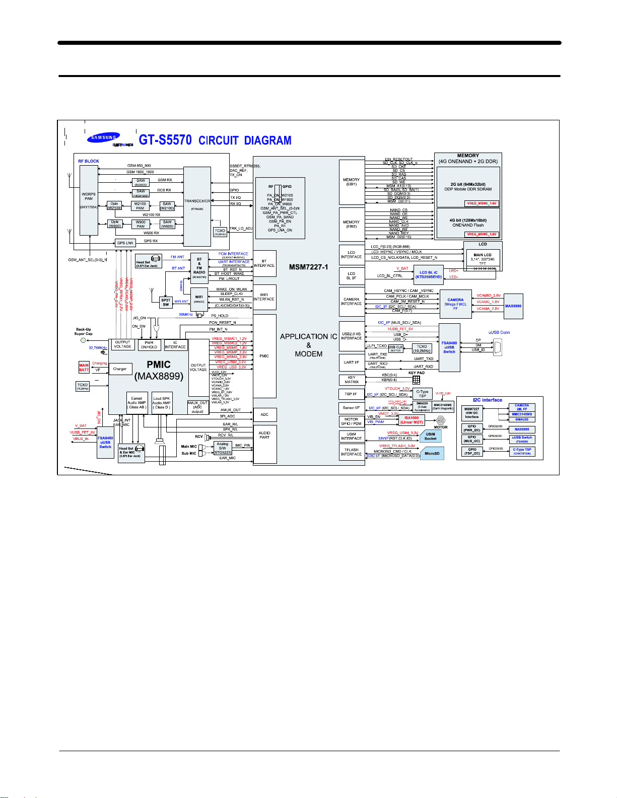
8.
Block Diagram
8-1.
Repair
3
8-1
SAMSUNG Proprietary-Contents may change without notice
This Document can not be used without Samsung's authorization
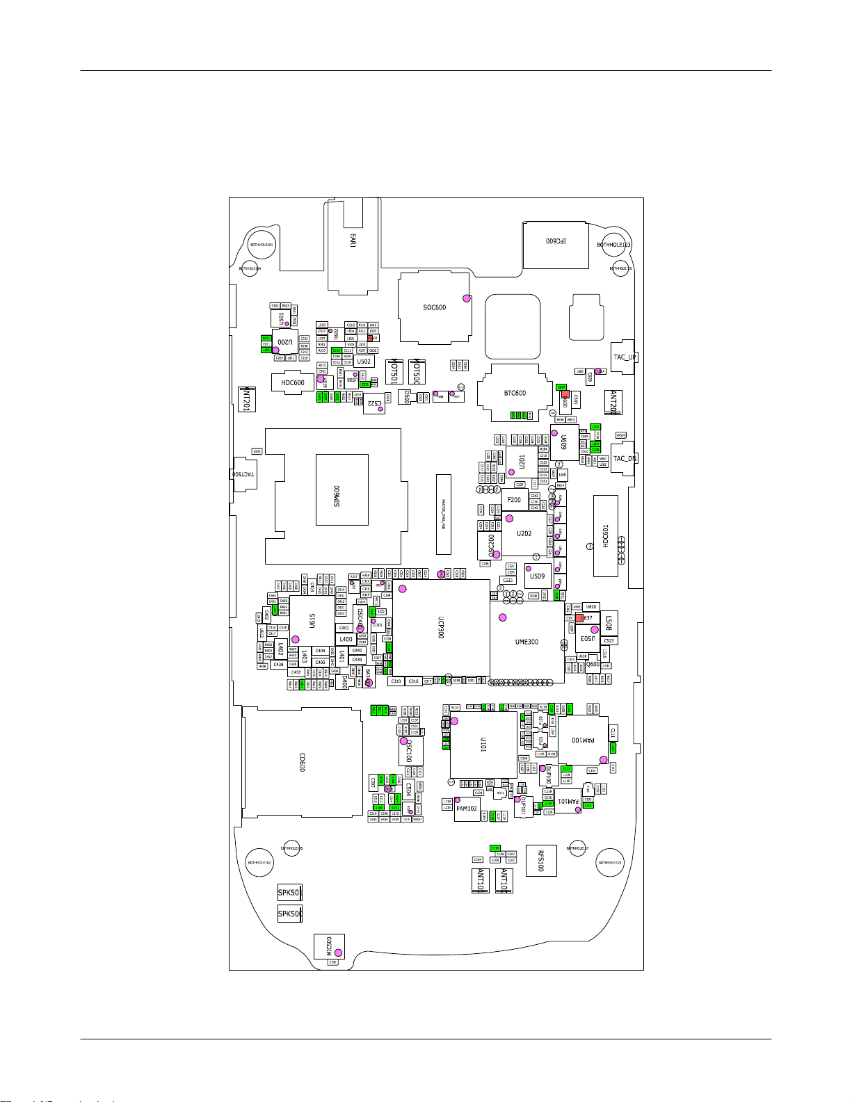
Level3Repair
PCB Diagrams (2010.12.22 Rev0.3)
8-2.
8-2-1.
Top
8-2
SAMSUNG Proprietary-Contents may change without notice
This Document can not be used without Samsung's authorization
 Loading...