

Page 1

9. Flow Chart of Troubleshooting
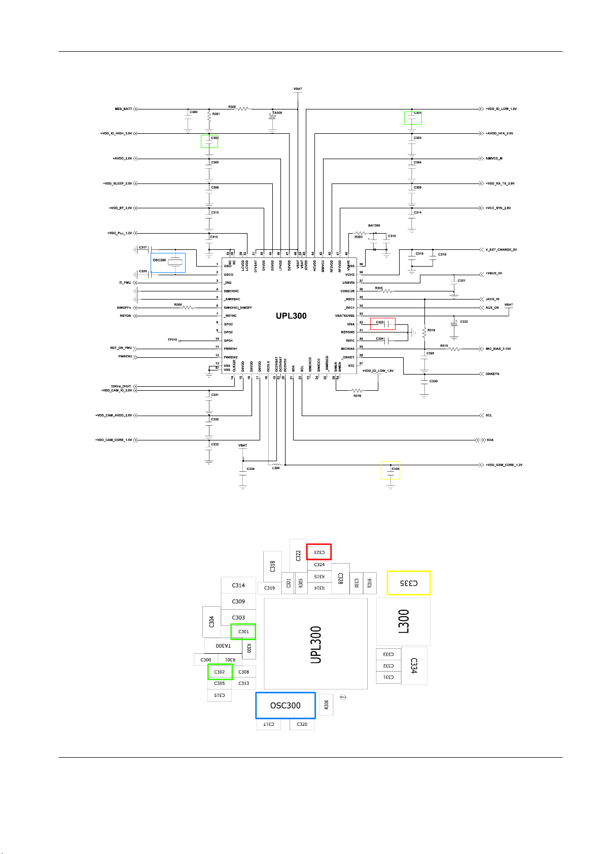
9-1. Power On
' Power On ' does not work
Yes
Check the Battery Voltage
is more than 3.4V
Yes
C323(VISA) = 2.7V?
Yes
Check the Clock at
OSC300=32KHZ
Yes
C301(+VDD_IO_LOW_1.8V) &
C302(+VDD_IO_HIGH_2.9V) =
"H"?
No
No
Change the Battery
Check the PMU related to VINT
No
Resolder OSC300
No
Check the related circuit
Yes
C335(+VDD_GSM_CORE_1.2V)
=1.2V?
Yes
Check the initial operation
Yes
END
No
9-1
SAMSUNG Proprietary-Contents may change without notice
This Document can not be used without Samsung's authorization
Check the +VDD_GSM_CORE_1.2V
circuit
Page 2
Flow Chart of Troubleshooting
9-2
SAMSUNG Proprietary-Contents may change without notice
This Document can not be used without Samsung's authorization
Page 3

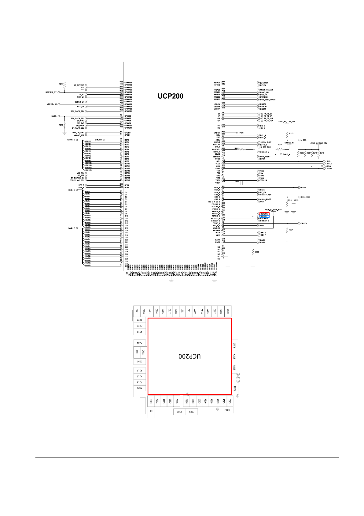
9-2. Initial
Flow Chart of Troubleshooting
Initial Failure
Yes
UCP200 pin C11 (RSTON) ="H"?
Yes
UCP200 pin F1(RSTEXTn) ="H"?
Yes
Check the 16bit data signal
&memoryCE
Yes
END
No
Check the circuit related to reset
No
Change UCP200
9-3
SAMSUNG Proprietary-Contents may change without notice
This Document can not be used without Samsung's authorization
Page 4
Flow Chart of Troubleshooting
9-4
SAMSUNG Proprietary-Contents may change without notice
This Document can not be used without Samsung's authorization
Page 5

9-3. Charging Part
Abnormal charging part
Flow Chart of Troubleshooting
Yes
Check the UPL300 pin 38
>4.9V
Yes
UPL300 pin 34(AUX_ON)
="L"?
Yes
Check the UPL300 pin 46
≒1.4V
Yes
END
No
No
No
Check the circuit related to
V_EXT_CHARGE_5V
Check the circuit related to
AUX_ON signal
Resolder or replace UPL300
9-5
SAMSUNG Proprietary-Contents may change without notice
This Document can not be used without Samsung's authorization
Page 6

Flow Chart of Troubleshooting
9-6
SAMSUNG Proprietary-Contents may change without notice
This Document can not be used without Samsung's authorization
Page 7
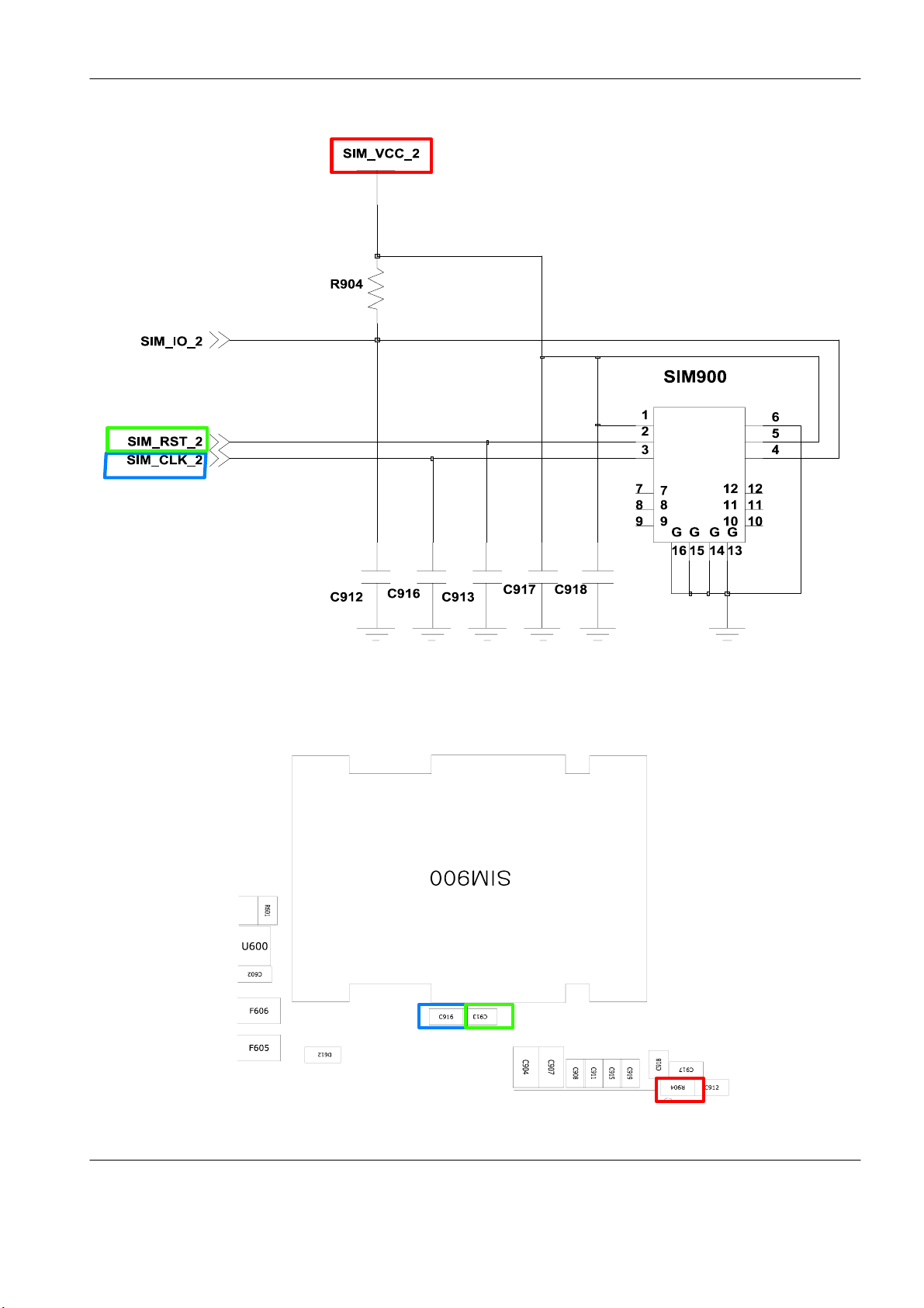
9-4. Sim Part
1)Master
Phone can't access SIM Card (slot1)
Yes
SIM300 pin 1,5 = "H"?
Yes
Flow Chart of Troubleshooting
No
Resolder or replace UPL300
After Power ON,
Check SIM_CLK_1 Signal on
pin3 of SIM300 in a few second
Yes
After SIM card insert,
SIM300 pin 2 = "H(SIM_RST_1)"?
Yes
Check the SIM Card
Yes
END
No
Check the Clock
No
Replace PBA
9-7
SAMSUNG Proprietary-Contents may change without notice
This Document can not be used without Samsung's authorization
Page 8

Flow Chart of Troubleshooting
9-8
SAMSUNG Proprietary-Contents may change without notice
This Document can not be used without Samsung's authorization
Page 9
2)Slave
Phone can't access SIM Card (slot2)
Yes
SIM900 pin 1,5 = "H"?
Yes
Flow Chart of Troubleshooting
No
Resolder or replace UPL900
After Power ON,
Check SIM_CLK_2 Signal on
pin3 of SIM900 in a few second
Yes
After SIM card insert,
SIM900 pin 2 = "H(SIM_RST_2)"?
Yes
Check the SIM Card
Yes
END
No
Check the Clock
No
Replace PBA
9-9
SAMSUNG Proprietary-Contents may change without notice
This Document can not be used without Samsung's authorization
Page 10
Flow Chart of Troubleshooting
9-10
SAMSUNG Proprietary-Contents may change without notice
This Document can not be used without Samsung's authorization
Page 11
9-5. Microphone Part
Microphone does not work
Flow Chart of Troubleshooting
Yes
Check the connection
fromMICtoAnalogs/w
Yes
Check the circuit
from UCP200 to MIC
Yes
Check the circuit
from UCP800 to MIC
Yes
Check the MIC
No
No
No
No
Resolder Analog s/w
(U401, U400)
Resolder the R400, R402, C401, C403,
R401, C402
Resolder the R411, R413, C406, C410,
R412, C409
Replace MIC
(Main Key PBA, HEA600)
Yes
END
9-11
SAMSUNG Proprietary-Contents may change without notice
This Document can not be used without Samsung's authorization
Page 12

Flow Chart of Troubleshooting
9-12
SAMSUNG Proprietary-Contents may change without notice
This Document can not be used without Samsung's authorization
Page 13

9-6. Speaker Part(Melody)
Speaker does not work
Yes
Flow Chart of Troubleshooting
U408 pin 7 = 2.9V?
Yes
Check input signal is ok ?
(When related function
operate)
Yes
Check output signal is ok ?
(When related function
operate)
Yes
Is Speaker working?
No
No
No
No
Check the PMU related to
+VDD_IO_HIGH_2.9V
Resolder C426, C430, L403, L404,
R419, R421, C427, C431
Resolder L401, L402
Change the Speaker(U407)
Yes
END
9-13
SAMSUNG Proprietary-Contents may change without notice
This Document can not be used without Samsung's authorization
Page 14

Flow Chart of Troubleshooting
9-14
SAMSUNG Proprietary-Contents may change without notice
This Document can not be used without Samsung's authorization
Page 15

9-7. Key Data Input
Check Initial Operation
Flow Chart of Troubleshooting
Yes
When one of the keys is
pushed,
is it displayed on LCD?
Yes
When one of the keys is
pushed,
KEY_COL(0:4),
KEY_ROW(0:4)
signal is OK?
Yes
END
No
Check the Key PBA, Dome sheet
&KeyPad
No
Replace the PBA
9-15
SAMSUNG Proprietary-Contents may change without notice
This Document can not be used without Samsung's authorization
Page 16

Flow Chart of Troubleshooting
9-8. Receiver Part
Receiver does not work
Is Receiver working?
Is Receiver working?
Yes
No
Resolder UCP200 or Change PBA
Yes
No
Replace the Receiver
END
Yes
9-16
SAMSUNG Proprietary-Contents may change without notice
This Document can not be used without Samsung's authorization
Page 17

9-9. Back Light (for Color Main LCD)
Backlight does not work
Yes
Flow Chart of Troubleshooting
Is LCD Contrast set on high
level in the Menu?
Yes
HEA601 pin 11 = H ?
Yes
Check I2C data is OK?
Yes
END
No
Set LCD Contrast on high level
No
Resolder HEA601 or change PBA
No
check related circuit from UCP200
9-17
SAMSUNG Proprietary-Contents may change without notice
This Document can not be used without Samsung's authorization
Page 18

Flow Chart of Troubleshooting
9-18
SAMSUNG Proprietary-Contents may change without notice
This Document can not be used without Samsung's authorization
Page 19

9-10. Key Back Light
Main Key LED does not work
Flow Chart of Troubleshooting
Yes
U600 pin 3(KEY_ON) = "H"?
Yes
U600 pin 1(VDD_KEY_3.3V)
=3.3V?
Yes
END
No
Check the UCP200 related to
"KEY_ON(GPIOA29)"
No
Change the U600
9-19
SAMSUNG Proprietary-Contents may change without notice
This Document can not be used without Samsung's authorization
Page 20

Flow Chart of Troubleshooting
9-20
SAMSUNG Proprietary-Contents may change without notice
This Document can not be used without Samsung's authorization
Page 21

9-11. Camera part
"Camera" function does not work
Flow Chart of Troubleshooting
Yes
Check the Camera
connector (CN500)
on LCD module
Yes
CN500 Pin 12 and Pin 14
=2.8V
Yes
CN500 Pin 16 = 1.5V
Yes
R518 or CN500 pin 3
=36MHz
Yes
Replace the camera
module
No
No
No
No
Reconnect the Camera module
Check the UPL300 related to
"VDD_CAM_IO_2.8V" and
"VDD_CAM_AVDD_2.8V"
Check the UPL300 related to
"VDD_CAM_CORE_1.5V"
Check U503 related to 36MHz
Yes
END
9-21
SAMSUNG Proprietary-Contents may change without notice
This Document can not be used without Samsung's authorization
Page 22

Flow Chart of Troubleshooting
9-22
SAMSUNG Proprietary-Contents may change without notice
This Document can not be used without Samsung's authorization
Page 23

9-12. GSM Receiver
1)Master
Flow Chart of Troubleshooting
RF input : CH center freq : +67.7kHz
RX ON
Cell Power : -60dBm
Yes
F101 pin13
≥ -65dBm
Yes
F101 pin1,2
≥ -68dBm
Yes
U100
pin24,25 ≥ -70dBm
Yes
U100 pin 4,5,6,7
≥0.2Vp_p
No
No
No
No
Resolder RFS100,C107,R101,R100
Check F101 pin9,12
Resolder C113, C121 L106
U100 pin11,12,16,
=L
32,33≥2.8V
pin10≥1.8V
Yes
No
No
Check ANT Switch
control circuit
Resolder F101
Check & Resolder
C128,C126,C125,C129
And PMU Part
Yes
Check UCP200
END
Yes
Resolder U100
9-23
SAMSUNG Proprietary-Contents may change without notice
This Document can not be used without Samsung's authorization
Page 24

Flow Chart of Troubleshooting
2)Slave
RF input : CH center freq : +67.7kHz
pinD6(PON_PA_S)=Low,
RX ON
Cell Power : -60dBm
Yes
PAM700 pin11
≥ -65dBm
Yes
PAM700 pin7
≥ -68dBm
Yes
U700
pin17,18≥ -70dBm
Yes
UCP800
pinC6(MOD_STANDBY
_S)=High,
pinA6(BAND_SEL_S)
=Low
No
No
No
No
RFS700,C705,L700,C711,
Resolder
L702,L704,R701,R702
Resolder PAM700
Resolder U700
Resolder UCP800
Yes
Check UCP200
END
9-24
SAMSUNG Proprietary-Contents may change without notice
This Document can not be used without Samsung's authorization
Page 25

9-13. GSM Transmitter
1)Master
TX ON (5Level)
Yes
F101 pin13
≥ 30dBm
Yes
F101 pin10
≥ 30dBm
No
No
Resolder RFS100,C107,R101,R100
Check F101
pin12 = H (2.6V),
Pin9 = L
Flow Chart of Troubleshooting
No
Check ANT Switch
control circuit
Yes
PAM100 pin11
≥ 30dBm
Yes
PAM100 pin7
≥-4dBm
Yes
U100 pin 4,5,6,7
≥0.2Vp_p
Yes
Check UCP200
No
No
No
Yes
Resolder or Change L109
Check PAM100
pin2,3,4,5,8 is ok?
Yes
U100 pin 11,12,16,
32,33≥2.8V
pin10≥1.8V
Yes
No
Change or Resolder F101
No
Resolder or Change PAM100
Check VBAT or PAM
control signal
Check U100
C128,C126,C125,C129
And PMU Part
Resolder U100
END
9-25
SAMSUNG Proprietary-Contents may change without notice
This Document can not be used without Samsung's authorization
Page 26

Flow Chart of Troubleshooting
2)Slave
TX ON (5Level)
Yes
PAM700 pin11
≥ 30dBm
Yes
PAM700 pin17
≥0dBm
Yes
U700pin 3,4,5,6
≥0.2Vp_p
Yes
Check UCP200
END
No
No
No
RFS700,C705,L700,C711,
Resolder
L702,L704,R701,R702
Resolder PAM700
Resolder U700
9-26
SAMSUNG Proprietary-Contents may change without notice
This Document can not be used without Samsung's authorization
Page 27

9-14. DCS Receiver
1)Master
Flow Chart of Troubleshooting
RF input : CH center freq : +67.7kHz
RX ON
Cell Power : -60dBm
Yes
F101 pin13
≥ -65dBm
Yes
F101 pin3,4
≥ -68dBm
Yes
U100
pin22,23 ≥ -70dBm
Yes
U100 pin 4,5,6,7
≥0.2Vp_p
No
No
No
No
Resolder RFS100,C107,R101,R100
Check F101 pin9,12
Resolder C110, C112, L105
=L
Yes
U100 pin11,12,16,
32,33≥2.8V
pin10≥1.8V
No
No
Check ANT Switch
control circuit
Resolder F101
Check & Resolder
C128,C126,C125,C129
And PMU Part
Yes
Check UCP200
END
Yes
Resolder U100
9-27
SAMSUNG Proprietary-Contents may change without notice
This Document can not be used without Samsung's authorization
Page 28

Flow Chart of Troubleshooting
2)Slave
RF input : CH center freq : +67.7kHz
RX ON
Cell Power : -60dBm
Yes
PAM700 pin11
≥ -65dBm
Yes
PAM700 pin6
≥ -68dBm
Yes
U700
pin15,16 ≥ -70dBm
Yes
No
No
No
RFS700,C705,L700,C711,
Resolder
L702,L704,R701,R702
Resolder PAM700
Resolder U700
UCP800
pinC6(MOD_STANDBY
_S)=High,
pinD6(PON_PA_S)=Low,
pinA6(BAND_SEL_S)
=High
Yes
Check UCP200
END
No
Resolder UCP800
9-28
SAMSUNG Proprietary-Contents may change without notice
This Document can not be used without Samsung's authorization
Page 29

9-15. DCS Transmitter
1)Master
TX ON (0Level)
Yes
Flow Chart of Troubleshooting
F101 Pin13
≥ 25dBm
Yes
F101 pin8
≥ 25dBm
Yes
PAM100 pin17
≥ 25dBm
Yes
PAM100 pin1
≤-4dBm
Yes
U100 pin 4,5,6,7
≥0.2Vp_p
No
No
No
No
No
Resolder RFS100,C107,R101,R100
Check F101
pin9= H (2.6V),
pin12 = L
Yes
Resolder or Change
C137
Check PAM100
pin2,3,4,5,8 is ok?
Yes
U100 pin11,12,17,
32,33 ≥2.8V
pin 10≥1.8V
No
No
No
Check ANT Switch
control circuit
Change or Resolder F101
Resolder or Change PAM100
Check +VBAT or PAM
control signal
Check & Resolder
C128,C126,C125,C129
And PMU Part
Yes
Check UCP200
END
Yes
9-29
SAMSUNG Proprietary-Contents may change without notice
This Document can not be used without Samsung's authorization
Resolder U100
Page 30

Flow Chart of Troubleshooting
2)Slave
TX ON (5Level)
Yes
PAM700 pin11
≥ 30dBm
Yes
PAM700 pin19
≥0dBm
Yes
U700pin 3,4,5,6
≥0.2Vp_p
Yes
Check UCP200
END
No
No
No
RFS700,C705,L700,C711,
Resolder
L702,L704,R701,R702
Resolder PAM700
Resolder U700
9-30
SAMSUNG Proprietary-Contents may change without notice
This Document can not be used without Samsung's authorization
Page 31

9-16. PCS Receiver
- Master only
Flow Chart of Troubleshooting
RF input : CH center freq : +67.7kHz
RX ON
Cell Power : -60dBm
Yes
F101 pin13
≥ -65dBm
Yes
F101 pin5,6
≥ -68dBm
Yes
U100
pin 20 ,21
≥ -70dBm
Yes
U100 pin 4,5,6,7
≥0.2Vp_p
No
No
No
Resolder RFS100,C107,R101,R100
Check F101 pin9,12
Resolder C105, C106, L101
=L
Yes
U100 pin11,12,17,
32,33≥2.8V
pin10≥1.8V
NoNo
Check ANT Switch
control circuit
Resolder F101
No
Check & Resolder
C128,C126,C125,C129
And PMU Part
Yes
Check UCP200
END
Yes
Resolder U100
9-31
SAMSUNG Proprietary-Contents may change without notice
This Document can not be used without Samsung's authorization
Page 32

Flow Chart of Troubleshooting
9-17. PCS Transmitter
- Master only
TX ON (0Level)
Yes
F101 pin13
≥ 25dBm
Yes
F101 pin8
≥ 25dBm
Yes
PAM100 pin17
≥ 25dBm
No
PAM100 pin1
≤-4dBm
Yes
U100 pin 4,5,6,7
≥0.2Vp_p
No
No
Yes
No
No
Resolder RFS100,C107,R101,R100
Check F101
pin9 = H (2.6V),
pin12 = L
Yes
Resolder or Change
C137
Check PAM100
pin2,3,4,5,8 is ok?
No
U100 pin11,12,16,
32,33≥2.8V
pin10≥1.8V
Yes
No
No
Check ANT Switch
control circuit
Change or Resolder F101
Resolder or Change PAM100
Check +VBAT or PAM
control signal
Check & Resolder
C128,C126,C125,C129
And PMU Part
Yes
Check UCP200
END
Yes
9-32
SAMSUNG Proprietary-Contents may change without notice
This Document can not be used without Samsung's authorization
Resolder U100
Page 33

[Master] Rx, Tx
Flow Chart of Troubleshooting
9-33
SAMSUNG Proprietary-Contents may change without notice
This Document can not be used without Samsung's authorization
Page 34

Flow Chart of Troubleshooting
9-34
SAMSUNG Proprietary-Contents may change without notice
This Document can not be used without Samsung's authorization
Page 35

[Slave] Rx, Tx
Flow Chart of Troubleshooting
9-35
SAMSUNG Proprietary-Contents may change without notice
This Document can not be used without Samsung's authorization
Page 36

Flow Chart of Troubleshooting
9-36
SAMSUNG Proprietary-Contents may change without notice
This Document can not be used without Samsung's authorization
Page 37

9-18. Bluetooth part
Bluetooth does not work
Flow Chart of Troubleshooting
Yes
F100 pin 2 ≥ -4dB
Yes
C100 (+position),
is ≥ 1.8V
Yes
C101, C102 is ≥ 3.0V
Yes
TP107, TP100, TP101
≥1.8V
BT100 pin A5
≥1.7V(32kHz)
No
No
No
No
Resolder or replace
C148, ANT100
Resolder C100 and
check the PMU part
Resolder C101, C102 check
or Replace BT100
Check or Replace BT100
Yes
Check UCP200
Yes
END
9-37
SAMSUNG Proprietary-Contents may change without notice
This Document can not be used without Samsung's authorization
Page 38

Flow Chart of Troubleshooting
9-38
SAMSUNG Proprietary-Contents may change without notice
This Document can not be used without Samsung's authorization
Page 39

9-19. FM Radio part
Radio does not work
C135, C136 = 2.9V
C131, L107 is OK?
Yes
Yes
No
No
Flow Chart of Troubleshooting
Resolder C135, C136 and
check the PMU part
Resolder C131, L107
Yes
Check UCP200
Yes
END
9-39
SAMSUNG Proprietary-Contents may change without notice
This Document can not be used without Samsung's authorization
Page 40

Flow Chart of Troubleshooting
9-40
SAMSUNG Proprietary-Contents may change without notice
This Document can not be used without Samsung's authorization
 Loading...