

Samsung 511-A, 611-A, 711-A, 811-A Service manual
DVD PLAYER
DVD-511A/518A/519A
DVD-611A/612A/615A/618A
DVD-711A/718A
DVD-811A/812A/818A/819A
DVD-518JA/618JA/818JA
DVD-618KA/718KA/818KA
SERVICE
1. Precautions
2. Troubleshooting
3. Exploded Views and Parts List
4. Electrical Parts List
5. Block Diagrams
6. PCB Diagrams
7. Wiring Diagrams
8. Schematic Diagrams
Manual
DVD PLAYER CONTENTS
SERVICE MANUAL DVD-511A/611A/711A/811A/618KA/718KA/818KA
DVD-711A/718A/811A/812A/818A/819A/818JA
DVD-711A (U.S.A/CANADA ONLY)
PLAY/PAUSE
OPEN/CLOSE
SKIPSTOP
STANDBY/ON
PLAY/PAUSE
OPEN/CLOSE
SKIPSTOP
STANDBY/ON
PHONES LEVEL
MIN MAX
OPEN/
CLOSE
SKIPSTOPPLAY/PAUSE
OPEN/CLOSE
DIGITAL VIDEO
STANDBY/ON
DIGITAL VIDEO
OPEN/
CLOSE
SKIPSTOPPLAY/PAUSE
OPEN/CLOSE
STANDBY/ON
DVD-611A/615A/618A
DVD-511A/518A/518JA/519A
DVD-612A/618JA
OPEN/
CLOSE
SKIPSTOPPLAY/PAUSE
OPEN/CLOSE
DIGITAL VIDEO
STANDBY/ON
DIGITAL VIDEO
PHONE
LEVEL
MIN MAX
OPEN/
CLOSE
SKIPSTOPPLAY/PAUSE
OPEN/CLOSE
DIGITAL VIDEO
STANDBY/ON
DIGITAL VIDEO
MIC1 MIC2 VOLUME
MIN MAX
DIGITAL ECHO
MIN MAX
PLAY/PAUSE
OPEN/CLOSE
SKIPSTOP
STANDBY/ON
MIC1 MIC2 VOLUME
MIN MAX
DIGITAL ECHO
MIN MAX
DVD-718KA/818KA
DVD-618KA
ELECTRONICS
© Samsung Electronics Co., Ltd. DEC. 2000
Printed in Korea
AH68-00706A

SERVICE NOTICE
MODEL NUMBER
BUYER NAME
2 CHIP MARKING
◆ This Service Manual is only for 2 chip (Main PCB) Model.
- 2 chip (Super chip) ; RIC1, SIC1
- 3 chip ; RIC1, SIC1, DIC1
◆ It is possible to identify 2 chip model throush the Model N0. on “Label-Rating” of
rear unit as shown below.
How to identify
3 chip Model
2 chip Model
◆ Refer to the Service Manual of 3 chip model for “Product Specification” and
“Disassembly and Reassembly”.

Samsung Electronics 1-1
1. Precautions
1-1 Safety Precautions
1) Before returning an instrument to the customer,
always make a safety check of the entire instrument,
including, but not limited to, the following items:
(1) Be sure that no built-in protective devices are
defective or have been defeated during servicing.
(1)Protective shields are provided to protect both
the technician and the customer. Correctly replace
all missing protective shields, including any
remove for servicing convenience.
(2)When reinstalling the chassis and/or other assembly in the cabinet, be sure to put back in place
all protective devices, including, but not limited to,
nonmetallic control knobs, insulating fish papers,
adjustment and compartment covers/shields, and
isolation resistor/capacitor networks. Do not operate this instrument or permit it to be operated without all protective devices correctly installed and
functioning.
(2) Be sure that there are no cabinet openings through
which adults or children might be able to insert
their fingers and contact a hazardous voltage. Such
openings include, but are not limited to, excessively wide cabinet ventilation slots, and an improperly fitted and/or incorrectly secured cabinet back
cover.
(3) Leakage Current Hot Check-With the instrument
completely reassembled, plug the AC line cord
directly into a 120V AC outlet. (Do not use a isolation transformer during this test.) Use a leakage
current tester or a metering system that complies
with American National Standards institute (ANSI)
C101.1 Leakage Current for Appliances and
Underwriters Laboratories (UL) 1270 (40.7). With
the instrument’s AC switch first in the ON position
and then in the OFF position, measure from a
known earth ground (metal water pipe, conduit,
etc.) to all exposed metal parts of the instrument
(antennas, handle brackets, metal cabinets, screwheads, metallic overlays, control shafts, etc.), especially any exposed metal parts that offer an electrical return path to the chassis.
Any current measured must not exceed 0.5mA.
Reverse the instrument power cord plug in the outlet and repeat the test. See Fig. 1-1.
Any measurements not within the limits specified
herein indicate a potential shock hazard that must
be eliminated before returning the instrument to
the customer.
Fig. 1-1 AC Leakage Test
(4) Insulation Resistance Test Cold Check-(1) Unplug
the power supply cord and connect a jumper wire
between the two prongs of the plug. (2) Turn on the
power switch of the instrument. (3) Measure the
resistance with an ohmmeter between the
jumpered AC plug and all exposed metallic cabinet
parts on the instrument, such as screwheads,
antenna, control shafts, handle brackets, etc. When
an exposed metallic part has a return path to the
chassis, the reading should be between 1 and 5.2
megohm. When there is no return path to the chassis, the reading must be infinite. If the reading is
not within the limits specified, there is the possibility of a shock hazard, and the instrument must be
re-pared and rechecked before it is returned to the
customer. See Fig. 1-2.
Fig. 1-2 Insulation Resistance Test
DEVICE
UNDER
TEST
(READING SHOULD
NOT BE ABOVE
0.5mA)
LEAKAGE
CURRENT
TESTER
EARTH
GROUND
TEST ALL
EXPOSED METER
SURFACES
ALSO TEST WITH
PLUG REVERSED
(USING AC ADAPTER
PLUG AS REQUIRED)
2-WIRE CORD
Antenna
Terminal
Exposed
Melal Part
ohm
ohmmeter

Precautions
1-2 Samsung Electronics
2) Read and comply with all caution and safety related notes non or inside the cabinet, or on the chassis.
3) Design Alteration Warning-Do not alter of add to
the mechanical or electrical design of this instrument. Design alterations and additions, including
but not limited to, circuit modifications and the
addition of items such as auxiliary audio output
connections, might alter the safety characteristics of
this instrument and create a hazard to the user. Any
design alterations or additions will make you, the
service, responsible for personal injury or property
damage resulting therefrom.
4) Observe original lead dress. Take extra care to
assure correct lead dress in the following areas:
(1) near sharp edges, (2) near thermally hot parts (be
sure that leads and components do not touch thermally hot parts), (3) the AC supply, (4) high voltage,
and (5) antenna wiring. Always inspect in all areas
for pinched, out-of-place, or frayed wiring, Do not
change spacing between a component and the
printed-circuit board. Check the AC power cord for
damage.
5) Components, parts, and/or wiring that appear to
have overheated or that are otherwise damaged
should be replaced with components, parts and/ or
wiring that meet original specifications.
Additionally, determine the cause of overheating
and/or damage and, if necessary, take corrective
action to remove any potential safety hazard.
6) Product Safety Notice-Some electrical and mechanical parts have special safety-related characteristics
which are often not evident from visual inspection,
nor can the protection they give necessarily be
obtained by replacing them with components rated
for higher voltage, wattage, etc. Parts that have special safety characteristics are identified by shading,
an ( )or a ( )on schematics and parts lists. Use
of a substitute replacement that does not have the
same safety characteristics as the recommended
replacement part might created shock, fire and/or
other hazards. Product safety is under review continuously and new instructions are issued whenever appropriate.

Precautions
Samsung Electronics 1-3
1-2 Servicing Precautions
CAUTION : Before servicing Instruments covered
by this service manual and its supplements, read and
follow the Safety Precautions section of this manual.
Note : If unforseen circument create conflict between
the following servicing precautions and any of the
safety precautions, always follow the safety precautions. Remember: Safety First.
1-2-1 General Servicing Precautions
(1) a. Always unplug the instrument’s AC power cord
from the AC power source before (1) re-moving
or reinstalling any component, circuit board,
module or any other instrument assembly, (2)
disconnecting any instrument electrical plug or
other electrical connection, (3) connecting a test
substitute in parallel with an electrolytic capacitor in the instrument.
b. Do not defeat any plug/socket B+ voltage inter-
locks with which instruments covered by this
service manual might be equipped.
c. Do not apply AC power to this instrument and
/or any of its electrical assemblies unless all
solid-state device heat sinks are correctly installed.
d. Always connect a test instrument’s ground lead
to the instrument chassis ground before connecting the test instrument positive lead. Always
remove the test instrument ground lead last.
Note : Refer to the Safety Precautions section ground
lead last.
(2) The service precautions are indicated or printed on
the cabinet, chassis or components. When servicing, follow the printed or indicated service precautions and service materials.
(3) The components used in the unit have a specified
flame resistance and dielectric strength.
When replacing components, use components
which have the same ratings. Components i-entified by shading, by( ) or by ( ) in the circuit diagram are important for safety or for the characteristics of the unit. Always replace them with the exact
replacement components.
(4) An insulation tube or tape is sometimes used and
some components are raised above the printed
wiring board for safety. The internal wiring is
sometimes clamped to prevent contact with heating components. Install such elements as they
were.
(5) After servicing, always check that the removed
screws, components, and wiring have been installed correctly and that the portion around the
serviced part has not been damaged and so on.
Further, check the insulation between the blades of
the attachment plug and accessible conductive
parts.
1-2-2 Insulation Checking Procedure
Disconnect the attachment plug from the AC outlet
and turn the power ON. Connect the insulation resistance meter (500V) to the blades of the attachment
plug. The insulation resistance between each blade of
the attachment plug and accessible conductive
parts(see note) should be more than 1 Megohm.
Note : Accessible conductive parts include metal panels, input terminals, earphone jacks, etc.

Precautions
1-4 Samsung Electronics
1-3 ESD Precautions
Electrostatically Sensitive Devices (ESD)
Some semiconductor (solid state) devices can be damaged easily by static electricity.
Such components commonly are called Electrostatically Sensitive Devices(ESD). Examples of typical ESD
devices are integrated circuits and some field-effect
transistors and semiconductor chip components. The
following techniques should be used to help reduce
the incidence of component damage caused by static
electricity.
(1) Immediately before handling any semiconductor
component or semiconductor-equipped assembly,
drain off any electrostatic charge on your body by
touching a known earth ground. Alternatively,
obtain and wear a commercially available discharging wrist strap device, which should be
removed for potential shock reasons prior to applying power to the unit under test.
(2) After removing an electrical assembly equipped
with ESD devices, place the assembly on a conductive surface such as aluminum foil, to prevent electrostatic charge buildup or exposure of the assembly.
(3) Use only a grounded-tip soldering iron to solder or
unsolder ESD devices.
(4) Use only an anti-static solder removal devices.
Some solder removal devices not classified as
“anti-static” can generate electrical charges sufficient to damage ESD devices.
(5) Do not use freon-propelled chemicals. These can
generate electrical charges sufficient to damage
ESD devices.
(6) Do not remove a replacement ESD device from its
protective package until immediately before your
are ready to install it.(Most replacement ESD
devices are packaged with leads electrically shorted together by conductive foam, aluminum foil or
comparable conductive materials).
(7) Immediately before removing the protective ma-
terials from the leads of a replacement ESD device,
touch the protective material to the chassis or circuit assembly into which the device will be
installed.
CAUTION : Be sure no power is applied to the chassis or circuit, and observe all other safety precautions.
(8) Minimize bodily motions when handling unpack-
aged replacement ESD devices. (Otherwise harmless motion such as the brushing together of your
clothes fabric or the lifting of your foot from a carpeted floor can generate static electricity sufficient
to damage an ESD device).

Precautions
Samsung Electronics 1-5
1-4 Handling the optical pick-up
The laser diode in the optical pick up may suffer electrostatic breakdown because of potential static electricity from clothing and your body.
The following method is recommended.
(1) Place a conductive sheet on the work bench (The
black sheet used for wrapping repair parts.)
(2) Place the set on the conductive sheet so that the
chassis is grounded to the sheet.
(3) Place your hands on the conductive sheet(This
gives them the same ground as the sheet.)
(4) Remove the optical pick up block
(5) Perform work on top of the conductive sheet. Be
careful not to let your clothes or any other static
sources to touch the unit.
◆ Be sure to put on a wrist strap grounded to the
sheet.
◆ Be sure to lay a conductive sheet made of copper etc.
Which is grounded to the table.
Fig.1-3
(6) Short the short terminal on the PCB, which is in-
side the Pick-Up ASS’Y, before replacing the PickUp. (The short terminal is shorted when the PickUp Ass’y is being lifted or moved.)
(7) After replacing the Pick-up, open the short termi-
nal on the PCB.
THE UNIT
WRIST-STRAP
FOR GROUNDING
1M
1M
CONDUCTIVE SHEET
Precautions
1-6 Samsung Electronics
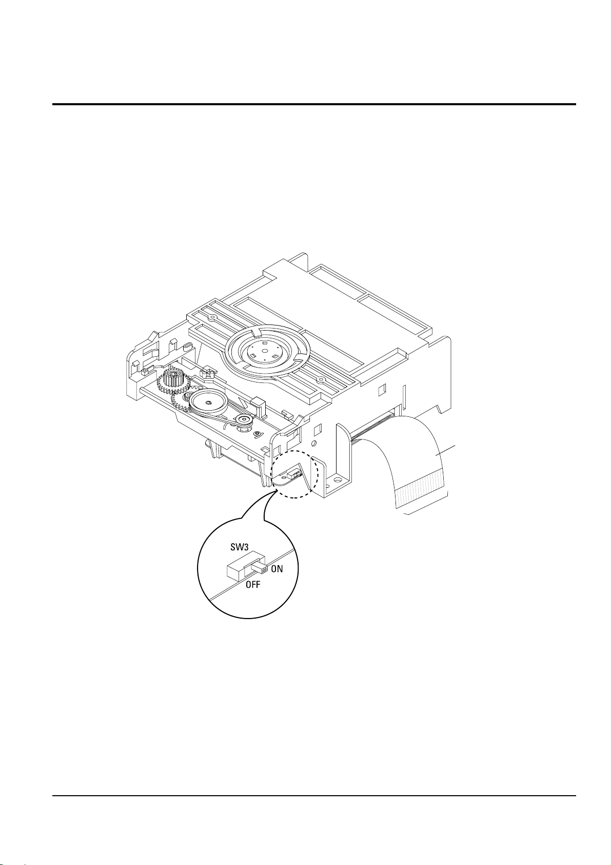
1-5 Pick-up disassembly and reassembly
1-5-1 Disassembly
1) Remove the power cable.
2) Switch SW3 on Deck PCB to “OFF” before
removing the Flat-Cable.
( Inserted into Main PCB DCN1. See Fig. 1-4)
3) Disassemble the Deck.
4) Disassemble the Deck PCB.
1-5-2 Assembly
1) Replace the Pick-up.
2) Assemble the Deck PCB.
3) Reassemble the Deck.
4) Insert Flat-Cable into Main PCB DCN1 and switch
SW3 on Deck PCB to “ON”. (See Fig 1-4)
FLAT-CABLE
TO MAIN PCB
(DCN1)
Note : If the assembly and disassembly are not done in correct sequence, the Pick-up may be damaged.
Fig. 1-4
Samsung Electronics 2-1
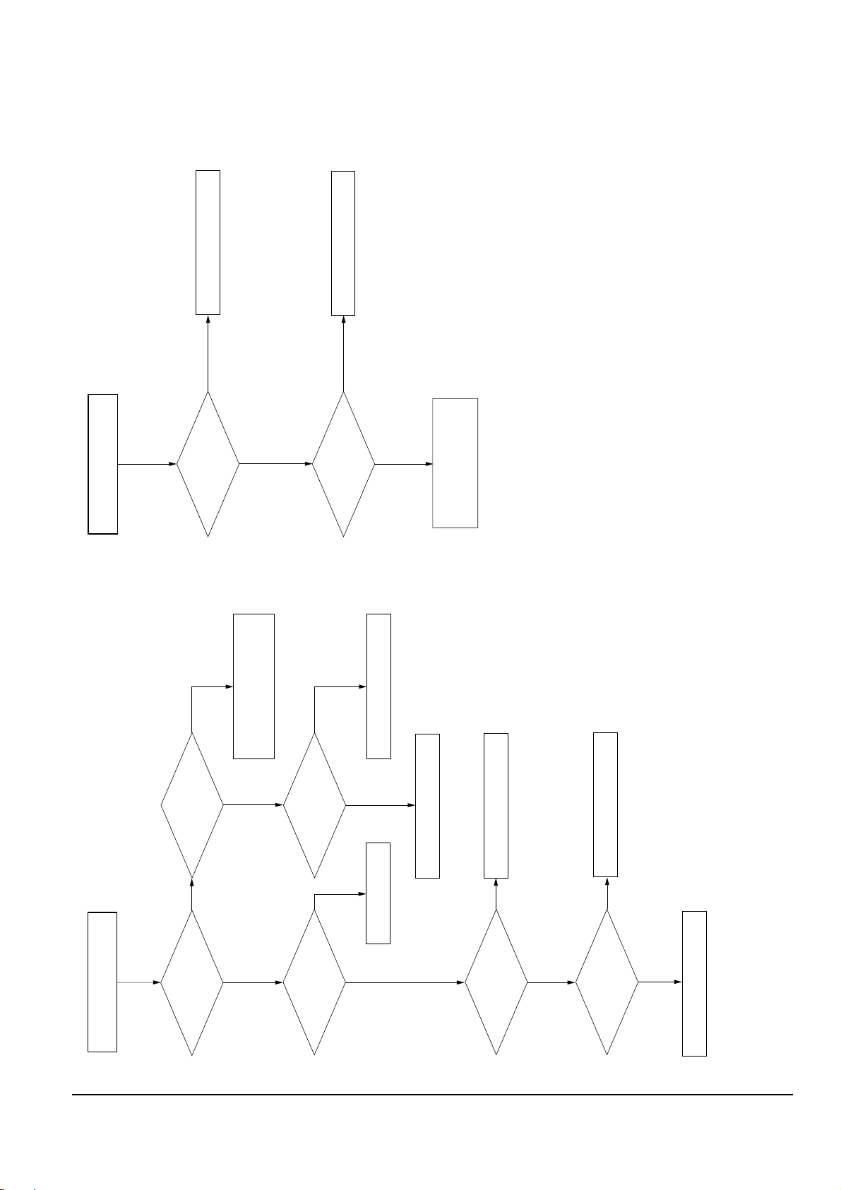
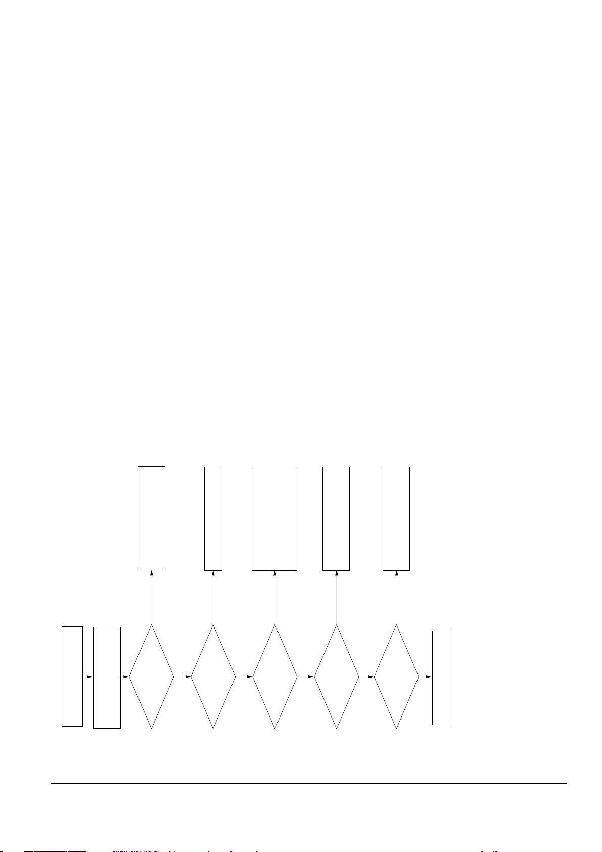
2. Troubleshooting
No Disc recognition
LD is outputted
from object lens at
play key input?
No focus incoming and
no disc occurs.
Yes
No
B
A
No focus incoming
FE in SIC1-25
is within specified range?
SIC3-1, 2 output
are normal?
Check open state from
DRIC4 to pick-up.
Check RIC1 and A, B, C, D input.
Check SIC3
Yes
Yes
No
No
A

Troubleshooting
2-2 Samsung Electronics
No pick-up home positing
SLD, SIC1-34
output is normal?
Check the Sled Motor and connection
Check MIC1
Yes
No
LED+, SLED-
SIC3-32, 33 output are
normal?
Check SIC3
Yes
No
NO LD CD ON
RIC1-21 is 5V?
Current exceeds 0.1A?
LD out pick-up replace.
Open check in related circuit.
Check MIC1
Yes
Yes
Yes
No
No
Divide RQ1 emitter terminal
voltage and 5V real voltage
difference into 10ohm.
B
Troubleshooting
Samsung Electronics 2-3
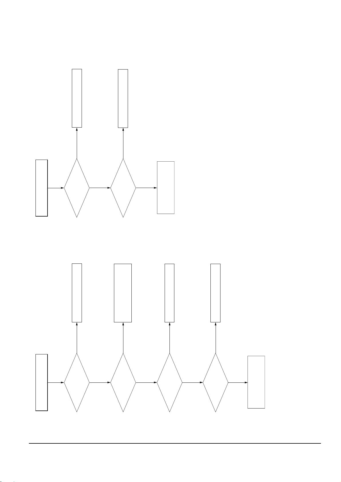
No Search Operation
MIRR, SIC1-157
output is normal?
Actual velocity occurs
at SIC1-34 terminal?
Actual velocity occurs
at SIC4-32, 33 terminal?
Check RIC1 peripheral circuit.
RFAGCO, RIC1-72
output level is normal?
Check SIC1 peripheral circuit.
Check SIC3 peripheral circuit.
No
No
No
No
Yes
TE occurs in
search range?
Focus On?
Yes
Yes
Yes
A
See "Fine Seek Check"
No
Yes
Check pick-up.
No
FINE SEEK Check
FINE SEEK MIRR
signal (RIC1-46) is missing?
TZCO signal
(SIC1-24) is occurs?
Track incomming is
delayed?
TE is within
2V and 3V?
Pick-up transfer smooth.
Check RIC1 Peripheral curcuit.
Check SIC1 Peripheral curcuit.
Time out due to many jump counts.
Check SIC1 peripheral circuit.
SIC1-33 output
is normal?
SIC3-28, 29
terminal outputs are
normal?
Check DCN1 and pick-up.
Check MECHA.
Check RIC1-26 terminal.
Check SIC3 peripheral circuit.
Yes
Yes
Yes
Yes
Yes
Yes
Yes
No
No
No
No
No
No
No
Troubleshooting
2-4 Samsung Electronics
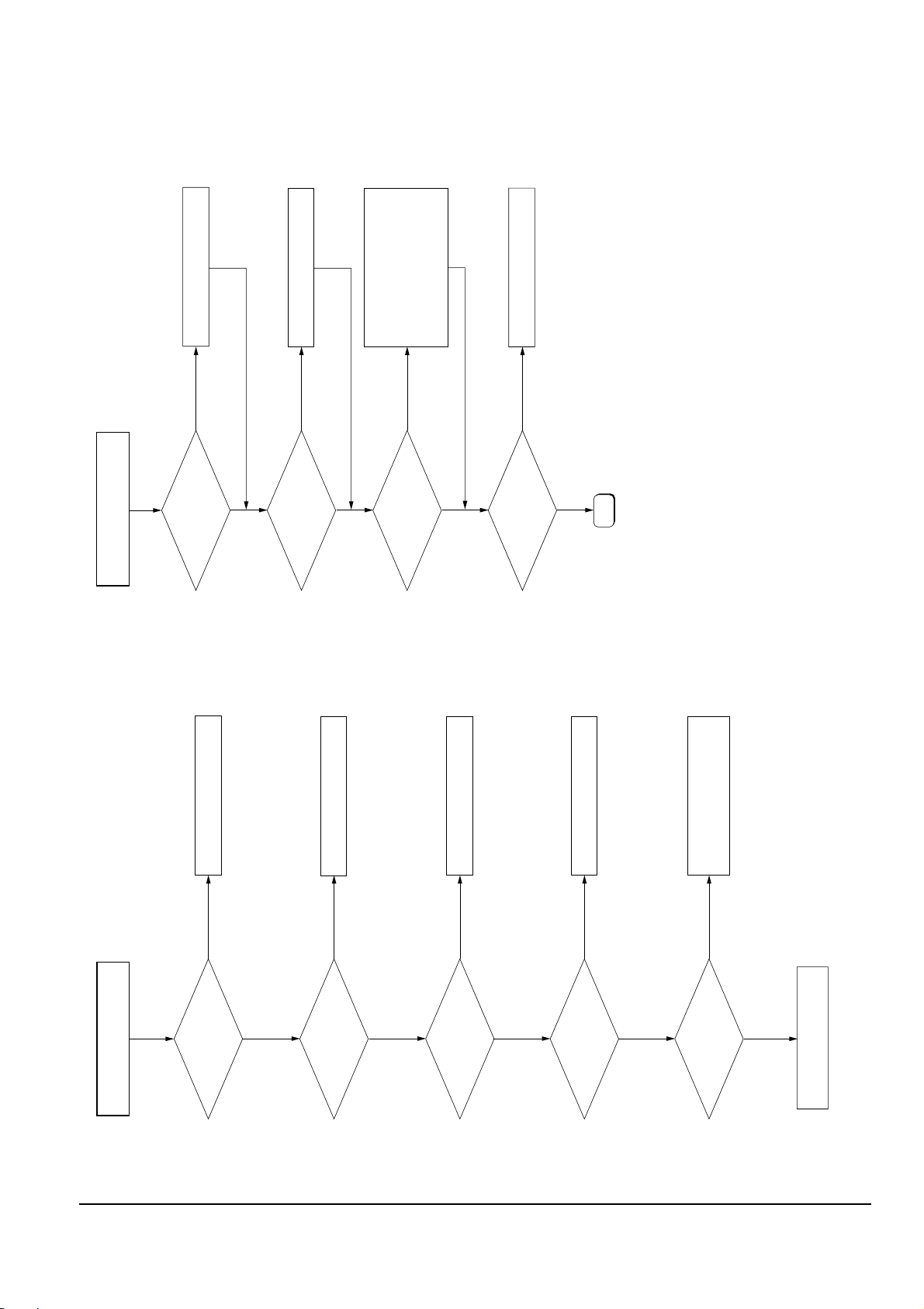
Abnormal rotation of
disc motor
Input of RF signal
is normal? (SIC1-15)
SPD output is normal?
(SIC1-35)
After resoldering SIC1.
SIC3-2 output (FG)
is normal?
SIC3-9 signal
MON is "H" ?
Check or replace disc motor.
Check SIC1, MIC1.
Check SIC3 soldering and power.
Check path to RIC1 and SIC1.
Check RIC1 soldering and power.
RIC1-70 output
are normal?
RIC1-71 output
is normal?
Check RIC1 peripheral
circuit and A, B, C, D.
Yes
Yes
Yes
Yes
Yes
Yes
No
No
No
No
No
No
No Tray open/close
MIC1-84, 85 is
Open ; "L", "L" ?
Close ; "H", "H"?
Check SIC3-35, 36
output at open/close
Check signal line state from
SIC3-35, 36 to tray motor.
Micom (MIC1) error.
Check SIC3.
Yes
Yes
No
No
Troubleshooting
Samsung Electronics 2-5
CD/VCD/DVD L/R output error
(Mixed Audio output)
Normal DATA 0 is
input in AIC1-7?
Analog output of
AIC1-20, 21, 22, 23 is
normal?
Check AVJ2 peripheral
soldering shot.
Check ZIC1-121 output.
Check ZIC1-125
(CD/VCD ; 16.9344MHz,
DVD ; 18.432MHz)
Yes
Yes
No
No
AOP1-1, 7 output
is normal?
Check AOP1 peripheral circuit.
Yes
No
Base terminal level
of AQ1, AQ3
are "L"?
Check FIC1-98 mute.
Yes
No
Digital output error
Output in ZIC1-127 is normal?
Output in
AIC3-6, 8, 10 is
normal?
Check AVJ4, ACJ5 peripheral
soldering shot.
Check ZIC1 peripheral circuit.
Check AIC3.
Yes
No
No
Yes
Troubleshooting
2-6 Samsung Electronics
No Power
(Standby LED OFF)
PFD01 error?
PDS01 voltage
is missing?
Replace PICF1.
Replace fuse.
Check PRF10.
No
No
Yes
PICF1 Drain (pin 1)
voltage is missing?
Check 2d voltage.
No
Voltage exists in
PICF1-4?
Check PRF11 ~ PRF14.
Yes
No
Pulse is missing
in PICF1-5?
Replace PICF1.
Check feed back.
Yes
Yes
No
Yes
All power is measured
correctly and front cable is
properly connected?
All clocks (20MHz,
33.8688MHz, 27MHz) of main PCB
oscillate normally?
Check A/V decoder signal process block.
Check all clock oscillating parts.
Yes
Yes
No
/CS2, /RD, /WR signal occur?
Check short pin out of micom
common-bus (8-bit).
Check short or operating of micom.
Check soldering of micom and
communication devices.
Yes
No
Play works?
Check ZIC1 peripheral unit.
Yes
No
Yes
Yes
Yes
Yes
C
Key operation or
remote control error

Troubleshooting
Samsung Electronics 2-7
MIC1-9 is fixed to 0V?
MIC7-4, 5 pin is fixed to 0V?
Check A/V decoder signal process block.
Check DVD signal process block.
Yes
Yes
MIC1-10, 19
waveform state (0, 1)
changes whenever pressing
front key?
Check MIC1 peripheral soldering.
Yes
Check eith article
"No Front (SET) Operation"
No
C
No
No
No front (SET) operation
REF +/-, 5V-all, -28V
power is supplied.
12MHz oscillation (FY1)?
If the problem persists ;
Check after replacing Jack PCB,
with another one.
Check other parts for abnormal
front operation persists.
Check power status.
Check X-TAL peripheral circuit.
Yes
Yes
No
No
Reset working in
FIC1-12?
Check reset peripheral circuit of FIC2.
Yes
No
FIC1 soldering is OK?
Check FIC1 soldering.
Yes
No
Key of STOP, PLAY, OPEN
work normally?
Check S/W interface.
Check communication status with
main micom
(Check FIC1 pins 27, 73, 74, 75, 95)
No
No
Troubleshooting
2-8 Samsung Electronics
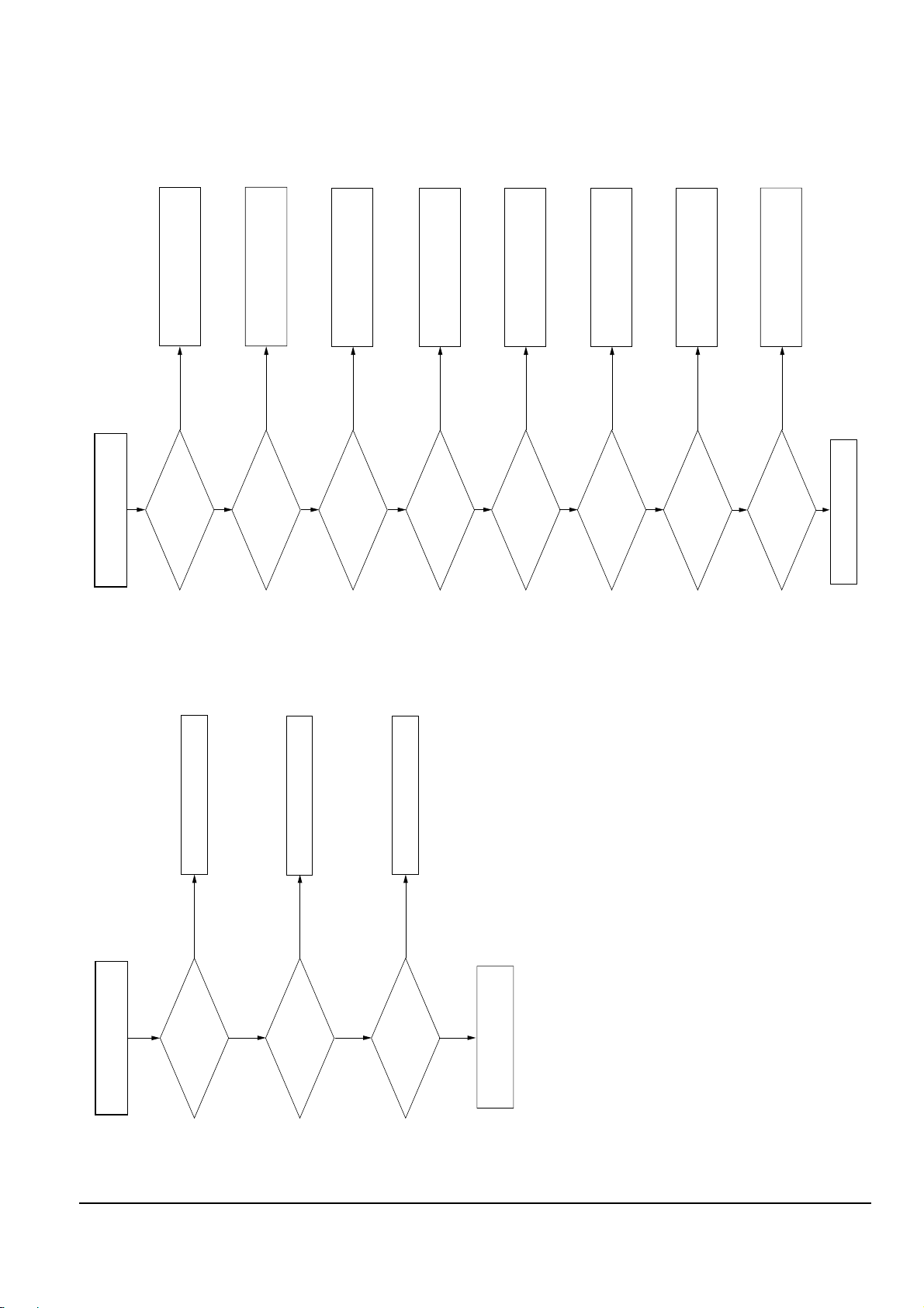
DVD play error
'NO DISK' appears
after pick-up moves up and
down twice at power on?
27MHz clock is
input in DIC1-14?
ZIC1 peripheral soldering
and short check.
Check DIC1, MIC1 peripheral short.
Check 27MHz oscillating part.
Yes
No
No
Signals are output
from SIC1-42, 44?
Replace SIC1.
Yes
No
Yes
CVBS output error
27MHz clock
input is normal at
pin 159 in ZIC1?
Analog output
is normal at pin 133
in ZIC1?
Check the connection between
pin 6 in ZIC4 and pin 129 in ZIC1.
Check the soldering of ZIC1.
Yes
Yes
No
No
Analog signals are
inputted normally
pin 7 in VIC1?
Yes
No
Power is
normal at pin 16
in VIC1?
Yes
No
Pin 1 in VIC1
is in low stste?
Yes
Check the connection netween
pin 133 in ZIC1 and VIC1.
Check the connection betwen
VIC1 and emitter of PQS58.
Check the connection between
pin 10 in FIC1 and pin 1 in VIC1.
Check the soldering of VIC1.
No
No
Check the connection between
VIC1 and output jack.
Pin of VDD_2.5 &
VDD-3.3 in Zic1 has
normal level?
Check the connection between
pin 1 in PCNS1 and pin 3 in ZIC5.
Yes
No
Peak to peak
voltage level of pin 10
in VIC1 is 2V?
Video signal of
about 1V appears at
output jack?
Yes
No
Yes
Check the RCA cable.
Troubleshooting
Samsung Electronics 2-9
RGB output error at SCJ1
Output voltage at
pin in SCJ1 is in
1V ~ 3V?
RGB signal is
outputed at pin 139, 145,
151 in ZIC1?
Check the pin 91 in FIC1 --> "H" state.
Check SCQ 15, 16 circuit.
See "Video output error in RCA jacks"
Yes
Yes
No
No
R signal is
outputed normally at pin 15
in SCIC3?
Yes
No
Yes
Œ
Check the connection between
pin 151 in ZIC1 and pin 2 in SCIC3.
´
Check the pin 9, 10, 11 in SCIC3
--> "L" state.
No
Check the connection with
pin 10, 13, 15 in SCIC6.
Check the connection with
pin 2, 4, 7 in VIC1.
RGB signal is
inputed at pin 2, 4, 7
in SCIC6?
RGB signal is
outputed at pin 7, 11, 15
in SCJ1?
No
Yes
Check the SCART cable.
Change the SCART output in
setup menu to RGB.

Troubleshooting
2-10 Samsung Electronics
MEMO
 Loading...