SAMSUNG 793DF Service Manual Troubleshooting
5 Troubleshooting
5-1 Parts Level Troubleshooting
Notes: Check the following circuits.
• No raster appears: Power circuit, Horizontal output circuit.
• High voltage develops but no raster appears: Video output circuits.
• High voltage does not develop: Horizontal output circuits.
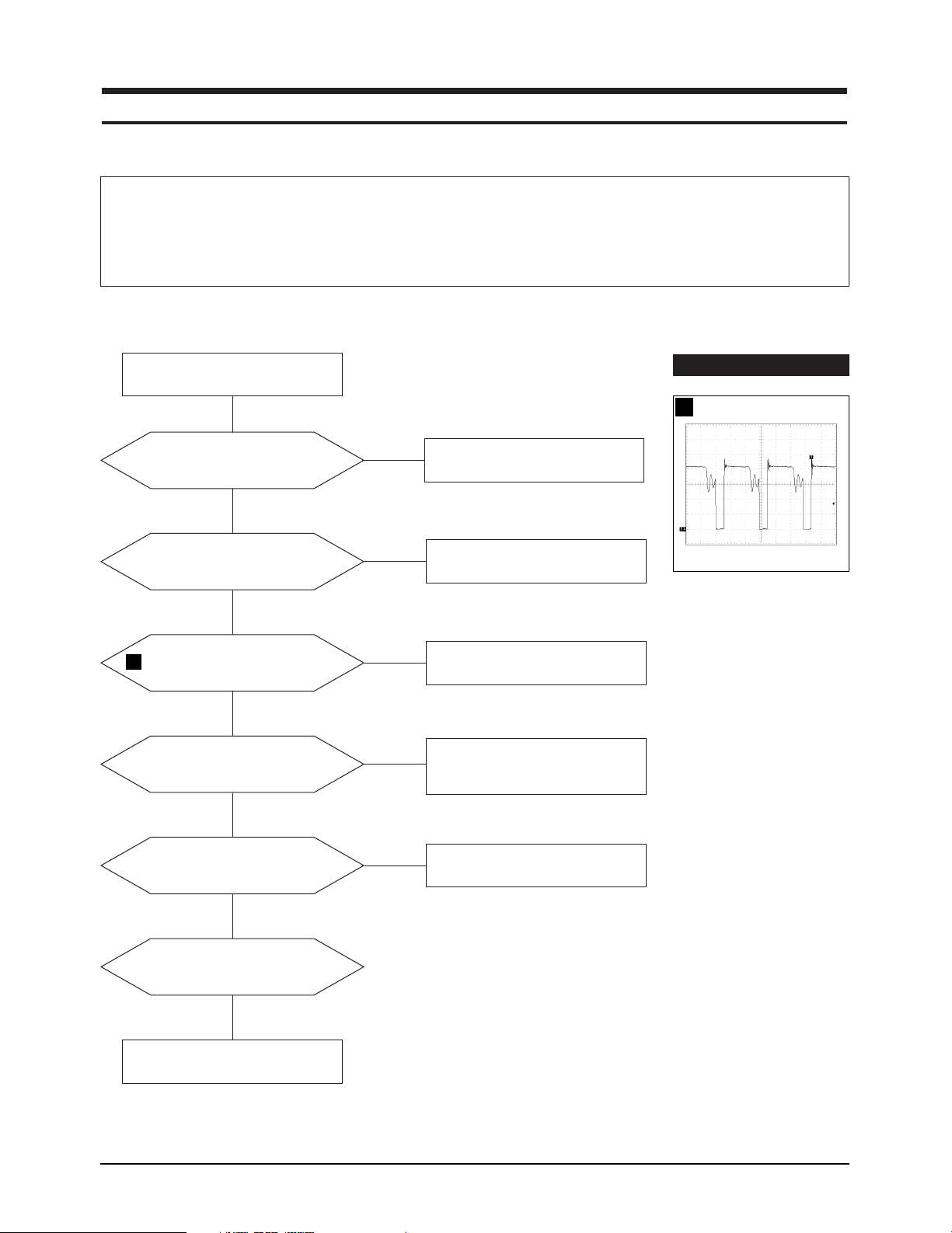
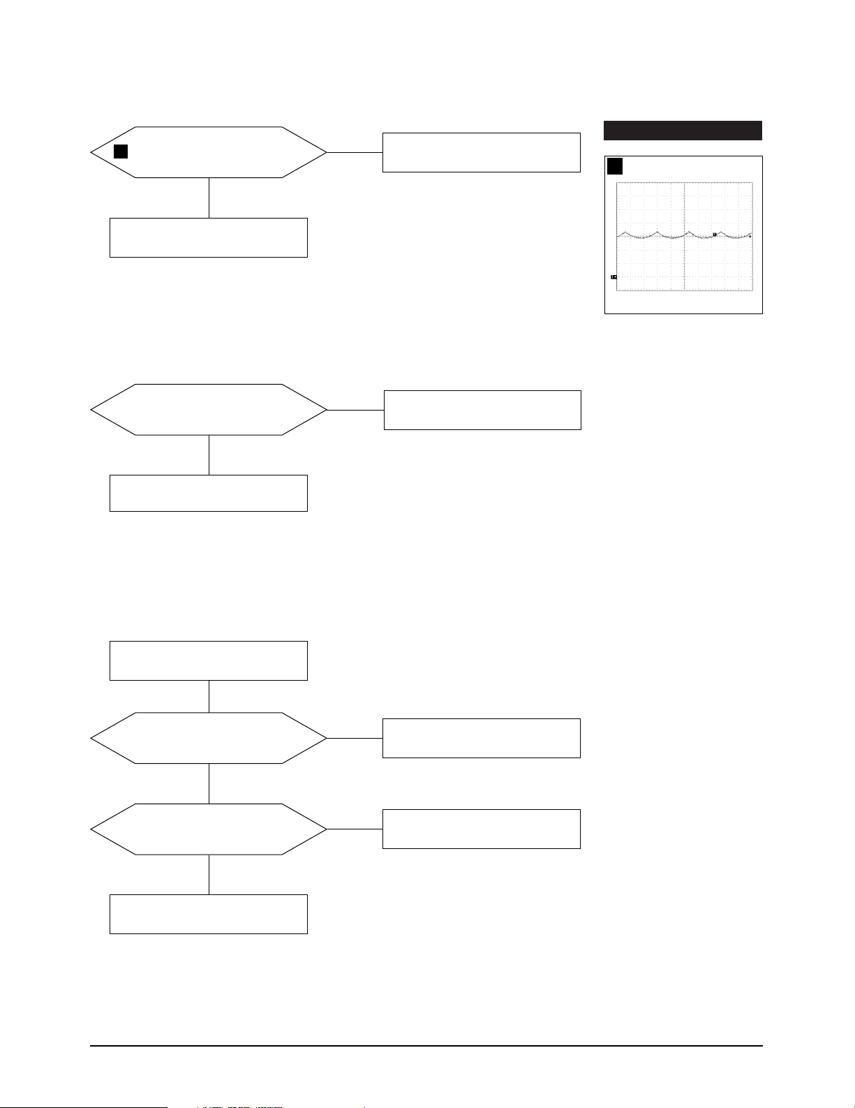
5-1-1 No Power Supply
Check and replace D601 and FH1
Chirping noise exists?
No
Repeating start?
No
1
IC601 Pin 1 waveform is right?
Yes
C627 Voltage is 13 V ± 0.5V?
Yes
Yes
No
No
Check and replace IC601.
Check and replace D606.
Check and replace IC601.
Check and replace IC201,
IC301, IC401, Q590, Q490,
and 12V regulator circuit.
WAVEFORMS
332 Vpp (IC601, #1)
1
Yes
Normal operation?
Yes
Verify voltages.
Done
LE15V*/LE17LS/LE17LT/
LE17KS/LE17KT/LE17JS/LE17JT
No
Replace main board.
5-1
5 Troubleshooting
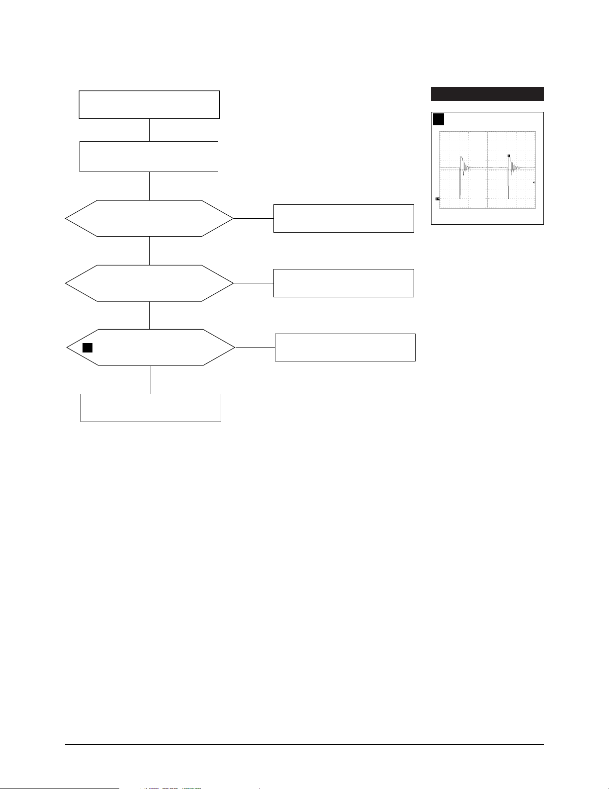
5-1-2 DPMS Failure
Check signal source
H/V sync. video level.
Make no H/V Sync. (power off mode)
LED blinks?
Yes
+12 V line off?
Yes
2
IC601 Pin 1 output
voltage exists?
Yes
No
No
No
Check IC201 Pin 40.
Check IC201 Pin 5/Pin 6 and
Q624, Q625 operation.
Refer to 5-1-1 no power supply.
WAVEFORMS
332Vpp (IC601, #1)
2
Done
5-2 LE15V*/LE17LS/LE17LT/
LE17KS/LE17KT/LE17JS/LE17JT
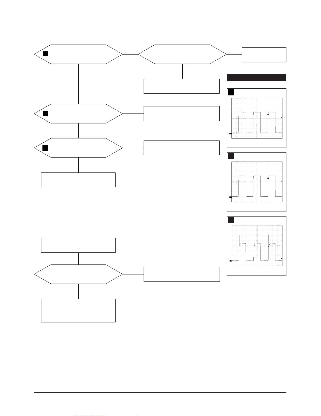
5-1-3 H_Deflection Failure
5 Troubleshooting
Does PWM output signal appear
3
at Pin 28 (B_DRV) of IC401?
Yes
Does horizontal pluse signal
4
appear at Pin 26 of IC401?
Yes
Does 110 Vp-p signal appear
5
at Collector of Q401?
Yes
Check Q590, Q490 and T401.
No
No
No
Does DC 12V appear at
Pin 29 of IC401?
Yes
Check IC401.
Check IC401.
Check Q401.
No
Check 12 V line.
WAVEFORMS
12 Vpp (IC401, #28)
3
2.00V (IC401, #26)
4
5-1-4 S Correction Failure
Check S1 ~ S3 signal.
S1~S3 signals are correct at each
frequency block?
Yes
Check and replace Q451, Q452,
Q453, Q454, Q458, Q457, Q456,
Q455, D451, D452, D453, D454.
No
Check and replace IC201.
78 Vpp (Q401, Collector)
5
LE15V*/LE17LS/LE17LT/
LE17KS/LE17KT/LE17JS/LE17JT
5-3
5 Troubleshooting
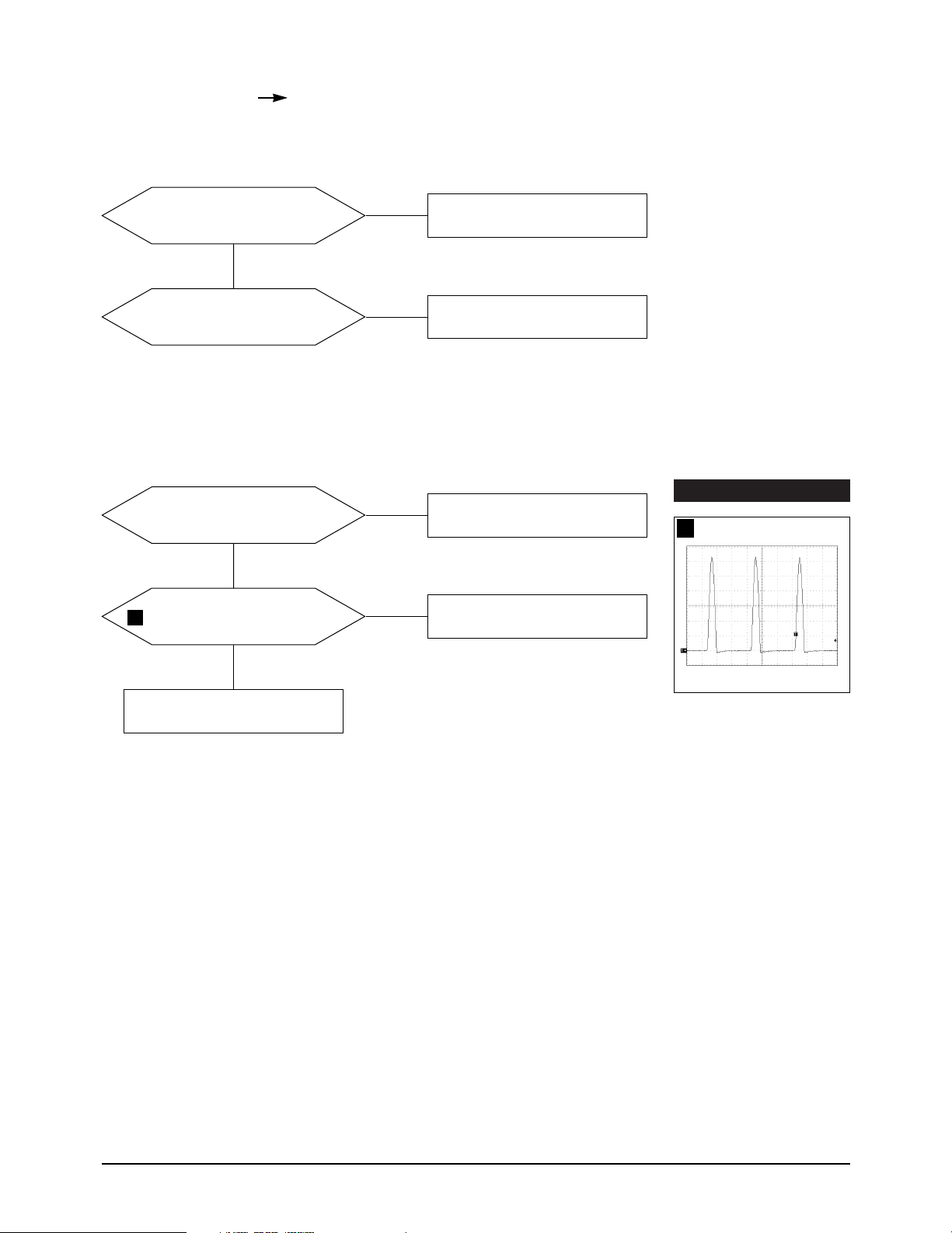
5-1-5 H_Lin. Failure Check and Replace L441 (Fix Type)
5-1-6 Invariable H_Size
IC401 Pin 28 voltage varies with
different B_DRV DAC values?
Yes
Q590 gate output duty varies with
different B_DRV DAC values?
5-1-7 Abnormal H_Size
IC401 Pin 24 output duty
varies with different B+ offset
DAC values?
Yes
6
Q490 collector
waveform is right?
No
No
No
No
Check and replace IC401.
Check some parts around Q590,
Pin 14~16 of IC401.
Check and replace IC201, IC401.
Check and replace Q411,
Q412, Q413, and Q414.
WAVEFORMS
1300 Vpp (Q490, Collector)
6
Yes
Check components
around D405 and L411.
5-4 LE15V*/LE17LS/LE17LT/
LE17KS/LE17KT/LE17JS/LE17JT
5-1-8 Side Pin or Trap Failure
5 Troubleshooting
7
IC401 Pin 24 output exists?
Yes
Refer to 5-1-7
abnormal H_Size
.
5-1-9 Para. or Pin Balance Failure
IC401 Pin 24 output varies with
different DAC values?
No
Replace IC401.
No
Yes
Check and replace IC401.
Refer to 5-1-7
abnormal H_Size
WAVEFORMS
0.44 Vpp (IC401, #24)
7
.
5-1-10 Tilt Failure ( Only 17” Function)
Check tilt connector connection
IC201 Pin 20 output duty varies
with different DAC values?
Yes
Q323 Base output varies with
different DAC values?
Yes
Check and replace Q321 and Q322.
No
Check and replace IC201.
No
Check and replace Q323.
LE15V*/LE17LS/LE17LT/
LE17KS/LE17KT/LE17JS/LE17JT
5-5
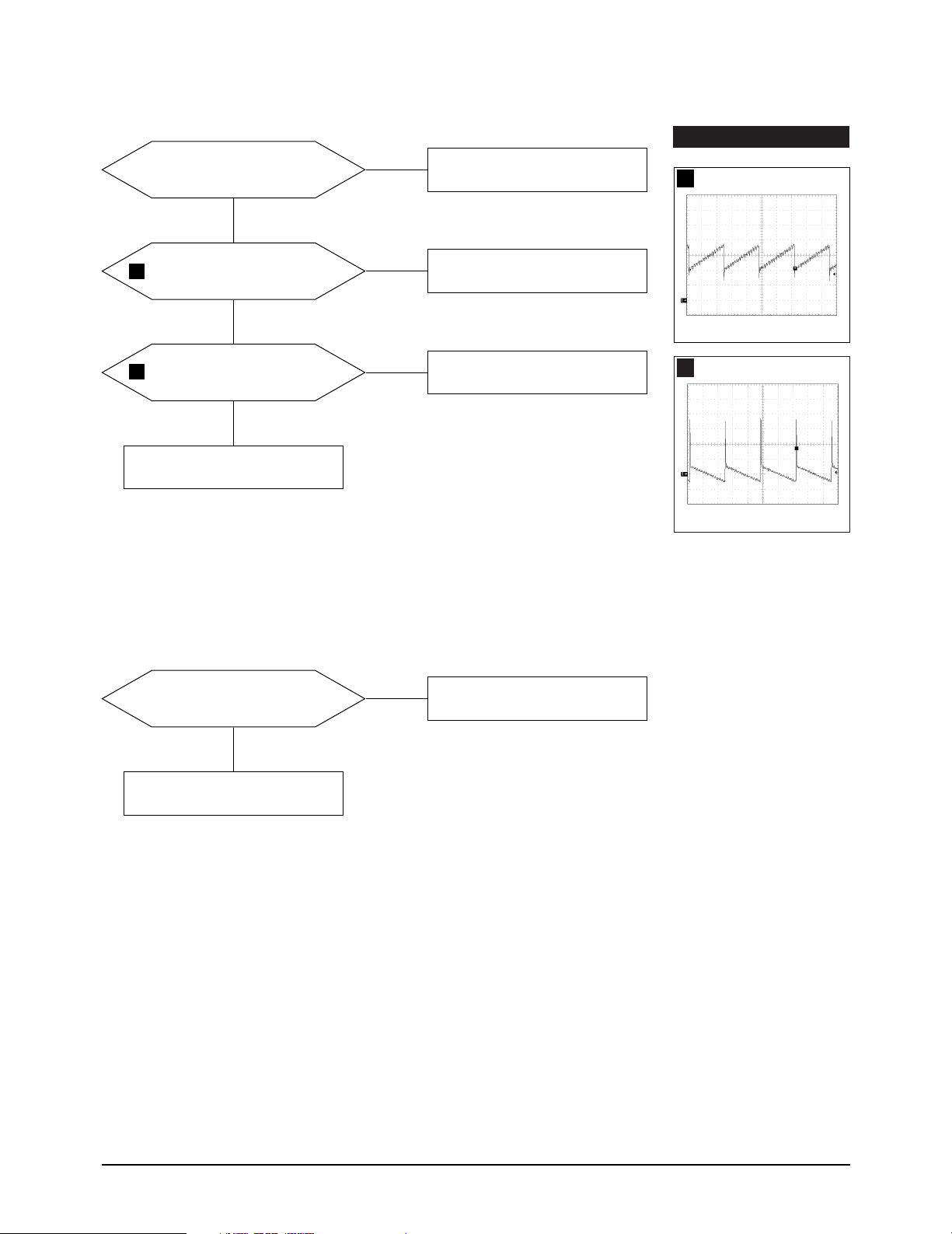
5 Troubleshooting
5-1-11 V Deflection Failure
13V and –10V lines are on?
Yes
No
Refer to 5-1-1 no power supply
WAVEFORMS
2.5 Vpp (IC401, #23)
8
IC401 Pin 23 output exists?
8
Yes
9
IC301 Pin 6 output exists?
Yes
Check DY connector connection.
No
No
5-1-12 V Size or Position Variation Failure
IC401 Pin 23 output varies with
different DAC values?
No
Check and replace IC401.
Check and replace
components around IC301.
Check and replace IC201 and IC401.
50 Vpp (IC301, #6)
9
Yes
Check and replace IC301.
5-6 LE15V*/LE17LS/LE17LT/
LE17KS/LE17KT/LE17JS/LE17JT
 Loading...