

S DU9435A
S amHop Microe lec tronics C orp.
Augus t , 2002
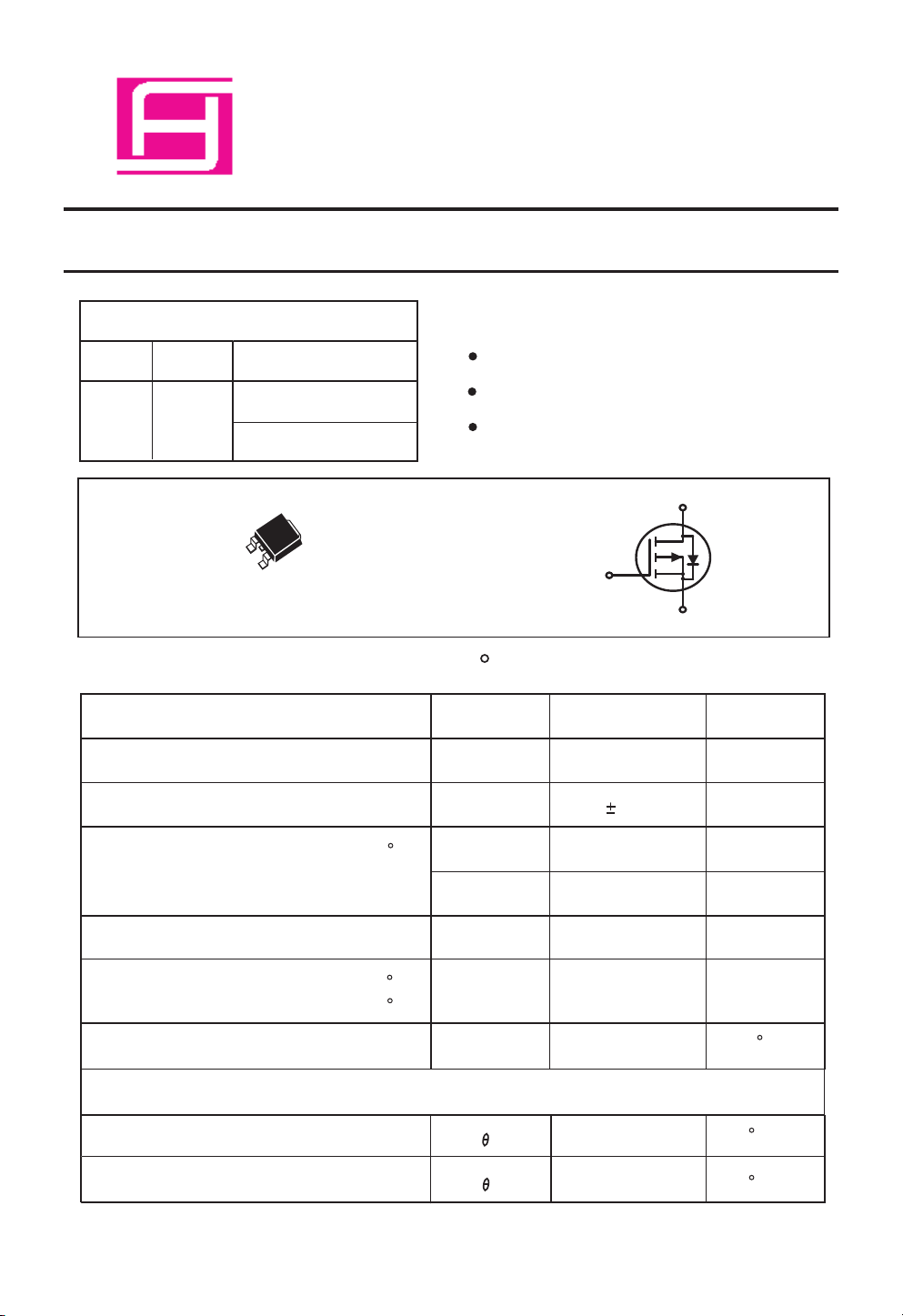
P -C hannel E nhancement Mode F ield E ffect T ransistor
PR ODUC T S UMMAR Y
VDS S
-30V
ID
-10A
R DS (O N) ( m
40 @ V GS = -10V
67 @ V GS = -4. 5V
G
S
S DU S E R IE S
TO -252AA (D-P AK )
W
) T YP
D
AB S OLUT E MAXIMUM R ATING S (TC=25 C unles s otherwise noted)
F E ATU R E S
S uper high dens e cell des ign for low R
R ugged and reliable.
TO-252 P acka ge.
D
G
S
DS (O N
).
P arameter
Drain-S ource Voltage
G ate-S ource Voltage 20
Drain C urrent-C ontinuous @ TJ =125 C
-P uls ed
a
Drain-S ource Diode F orward C urrent 1.9
Maximum P ower Diss ipation
@ T c=25 C
S ymbol
V
DS
V
G S
I
D
I
DM
I
S
P
D
-30
-10
-30
Derate above 25 C
Operating and S torage
Temperature R ange
TJ, T
S TG
-55 to 150
THE R MAL C HAR AC TE R IS TIC S
Therma l R es istance, J unction-to-C as e
Therma l R es istance, J unction-to-Ambient
R
R
J C
J A
Limit Unit
V
V
A
A
A
2. 5
3
50
W
C
C
C
/W
/W
1
S DU9435A
E LE C T R IC AL C HAR AC TE R IS T IC S (T C 25 C unles s otherwis e noted)
P arameter
S ymbol
=
C ondition
Min
Typ
C
Max
Unit
OF F C HAR AC TE R IS TIC S
5
V
G S
Drain-S ource B reakdown Voltage
Zero G ate Voltage Drain C urrent
G ate-B ody Leakage
ON C HAR AC TE R IS TIC S
b
G ate T hreshold Voltage
Drain-S ource On-S tate R es istance
On-S tate Drain C urrent
0V, ID -250uA
B V
DS S
I
DS S
I
G S S
V
G S (th)
R
DS (ON)
I
D(O N )
g
F S
c
VDS -24V, V
V
G S
V
DS VG S
V
G S
V
G S
V
DS
V
DS
=
=
= =
=
=
=
=
= -5V, V
= =
G S
20V, VDS 0V
, ID = -250uA
D
D
G S
D
=
=
= -10V
-10V, I
-4.5V, I
-15V, I
0V
=
-5.3A
-4.2A
- 5.3A
-30
-1 -1.5 -3
-20
40
67
9
-1
100
50
90
V
uA
nA
V
m-ohm
m-ohm
A
SF orward Trans conductance
DY NAMIC C HAR AC TE R IS TIC S
Input C apacitance
Output C apacitance
R everse Trans fer C apacitance
S WIT C HING C HAR AC TE R IS TIC S
Turn-On Delay T ime
R ise T ime
Turn-Off Delay T ime
F all T ime
Total G ate C ha rge
G ate-S ource C harge
G ate-Drain C harge
c
C
IS S
C
OS S
C
R S S
t
D(O N )
t
t
D(O F F)
t
Q
Q
Q
V
DS
f =1.0MH
VD = -15V,
r
f
ID = -1A,
V
G E N
R
G E N
VDS =-15V,ID = -5.3A,V
g
VDS =-15V,ID = -5.3A,V
gs
gd
VDS =-15V, ID = -5.3A,
V
G S
2
=-15V, V
Z
= - 10V,
= 6 -ohm
=-10V
G S
= 0V
G S
G S
=-10V
=-4.5V
860
470
180
20 ns
9
10 40
37
90
23 110
15
20
10.5
8.6
3
4
P
F
P
F
P
F
ns
ns
ns
nC
nC
nC
nC

S DU9435A
E LE C T R IC AL C HAR AC TE R IS T IC S (TC=25 C unles s otherwis e noted)
P arameter
S ymbol
C ondition
Min
Typ
C
Max
Unit
DR AIN-S OUR C E DIO DE C HAR AC T E R IS T IC S
Diode F orwa rd Voltage
Notes
a.P uls e Tes t:P uls e W idth 300us , Duty C ycle 2% .
b.G uaranteed by des ign, not s ubject to production tes ting.
25
-V GS =10, 9,8, 7V
20
15
10
5
-ID , Dra in C urrent (A )
0
0 0. 5 1. 0 1. 5 2. 0 2. 5 3 .0
-V DS , D rain-to-S ource Voltage (V)
F igure 1. O utput C hara cteris tics F igure 2. Trans fer C haracteris tics
V
S D
6V
5V
4V
3V
b
V
G S
= 0V, Is =-5. 3A
20
16
12
8
4
-ID , Dra in C urrent (A )
0
0 0 .5 1 1. 5 2 2. 5 3
-0.84
-55 C
25 C
T j=125 C
-V GS , Ga te-to-S ource Voltage (V )
-1.3
5
V
300 0
250 0
200 0
150 0
100 0
C , C apa citance (pF )
500
0
0 5 10 15 20 25 30
-V DS , D rain-to S ource Voltage (V)
F igure 3. C apa citance
C iss
C oss
C rss
1. 8
VGS =-1 0V
ID=-5. 3A
1. 6
1. 4
1. 2
1. 0
On-R es istance(O hms)
(N ormalize d)
0. 8
R DS (O N),
0. 6
-50 0 50 100 150
Tj, J unction T empera ture ( C )
F igure 4. O n-R es is tance Va ria tion with
Temperature
3

S DU9435A
1.09
VDS=V
1.06
1.03
1.00
5
0.97
Vth, Normalized
0.94
G a te-S ource T hre s hold V oltage
0.91
-50 -25 0 25 50 75 10 0 125 150
G S
ID=-250uA
Tj, J unction T empera ture ( C )
F igure 5. G ate T hres hold V ariation
with T emperature
15
12
9
6
1.15
ID=-250uA
1.10
1.05
1.00
0.95
0.90
B V DS S , Normaliz ed
0.85
Dra in-S ource B reakdown V oltage
-50 -25 0 25 50 75 100 125 150
Tj, J unction T empera ture ( C )
F igure 6. B rea kdown V oltage V ariation
with T emperature
20. 0
V
G S
=0V
10. 0
3
gFS , T rans conductance (S )
0
0 5 10 15 20
-ID S, Drain-S ource C urrent (A)
VDS=-15V
F igure 7. T ransconductance V a ria tion
with Drain C urrent
10
VDS=-15V
8
ID=-5. 3A
6
4
2
VG S, Gate to S ource V oltage (V )
0
0 2 4 6 8 10 12 14 16
Qg, T otal G ate C ha rge (nC )
F igure 9. G ate C harge
4
-Is , S ource-dra in curre nt (A)
1.0
0.4 0.6 0.7 0.9 1.1 1.3
-V S D, B ody D iode F orward Voltage ( V )
F igure 8. B ody Diode F orward V oltage
Variation with S ource C urrent
50
10
(O N) L imit
S
D
R
1
V
G S
0.1
-ID , D ra in C urrent (A)
0.03
=-10V
S ingle P ulse
TA=25 C
0.1 1 10 30 50
-V D S, Dra in-S ource V oltage (V )
10ms
100 m
s
1s
DC
F igure 10. Maximum S afe
O pera ting Area

S DU9435A
DD
-V
on
t
d(off)
t
r
d(on)
R
IN
V
V
G S
G EN
R
G
L
D
OU T
V
S
t
OU T
V
IN
V
10%
t
90%
10% 10%
50% 50 %
INV E R TE D
P ULS E W IDT H
90%
t
off
f
t
90%
6
F igure 11. S witching T est C ircuit
2
1
D=0. 5
0. 2
0. 1
0. 1
0. 05
0. 02
0. 01
-5
10
0. 01
S ING LE P UL S E
-4
10
r(t), Normalize d E ffective
T rans ient Thermal Impedanc e
F igure 13. N ormalized T hermal T rans ient Impeda nce C urve
F igure 12. S witching W aveforms
-3
10
S quare W ave P ulse Duration (s ec)
-2
10
DM
P
1
t
2
t
1. R θJA (t)=r (t) * R θJA
2. R θJA=S ee Data shee t
3. TJ M-T A = PDM* R θJA ( t)
4. Duty C ycle , D=t1/t2
-1
10
1 10
5
 Loading...