

Page 1
SE2522BL
RangeCharger™ 2.4GHz +23 dBm Power Amplifier
Preliminary Information
Applications
DSSS 2.4GHz WLAN (IEEE802.11b)
OFDM 2.4GHz WLAN (IEEE802.11g)
Access Points, PCMCIA, PC Cards
2.4GHz Cordless Telephones
Features
High output power amplifier
+23dBm P
+25dBm P
at 3.3V
1dB
at 3.3V
sat
Integrated Power Detector
Integrated control for output power and DC current
Single supply voltage: 2.7 to 3.6 V
Pin compatible with SiGe Semiconductor’s
SE2522L
Exceptional temperature stability <1dB output
power variation from –40 to +85°C
Small outline plastic package
Ordering Information
Type Package Remark
SE2522BL 3mm x 2mm
8 Pin QFN
Samples
Product Description
The SE2522BL is a 2.4GHz power amplifier. The device
is designed for use in the 2.4GHz ISM band for wireless
LAN and cordless telephone applications. It incorporates
a power detector for closed loop monitoring of output
power.
For wireless LAN applications, the device meets the
requirements of IEEE802.11b and delivers
approximately +23dBm @ ACPR = -30dBc. In
IEEE802.11g applications the PA delivers approximately
16dBm.
For cordless telephone applications, the SE2522BL
delivers up to +25dBm saturated output power at 3.3V.
The SE2522BL includes a linear analog control (0.1 to
1.6V) for minimizing DC current consumption and
maximizing PAE.
The SE2522BL contains a digital enable for device on/off
control, ramping is typical 1 µsec.
The SE2522BL contains an integrated power detector
with an input power range of 15dB, and an accuracy of
± 1.0dB. An accurate automatic level control function can
easily be implemented using this detector circuit.
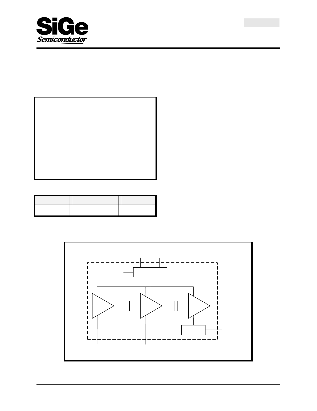
Functional Block Diagram
IN
Pre-
Driver
V
CC0
Stage 1
V
CC1
V
EN
Stage 2
Detector
OUT/V
V
DET
CC2
V
CTL
V
CC0
Bias Generator
61-DST-01 Rev 1.4 Dec 03/02 1 of 8
Page 2
RangeCharger™ 2.4GHz +23 dBm Power Amplifier
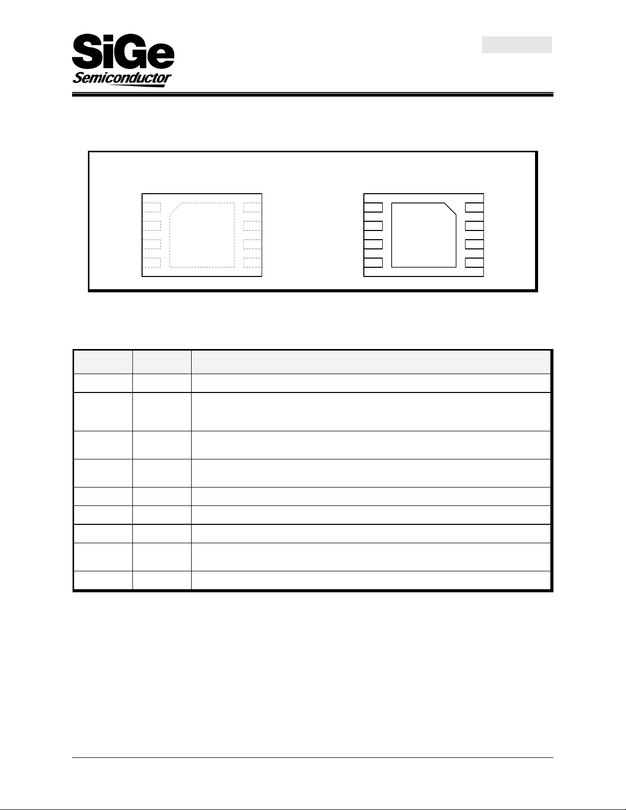
Pin Out Diagram
Note: Pads and die pad shown are at the bottom of package.
SE2522BL
Preliminary Information
Top View
OUT/V
CC2
NC
V
CC1
V
CC0
1
V
DET
2
3
4
2522BL
V
CTL
V
EN
IN
8
7
6
5
OUT/V
NC
V
CC1
V
CC0
CC2
Pin Out Description
Pin No. Name Description
1 V
2
3
4 IN
Analog power detector output
DET
Controls the RF output power and DC current level of the power amplifier. An analog
V
CTL
control signal between 0.1V and 1.6V varies the PA output power between Min. and
Max. values.
V
EN
Power Amplifier Enable pin. A digital control signal with logic high (power up) and
logic low (power down) is used to turn the device on and off.
Power amplifier RF input, external input matching network with DC blocking is
required.
Bottom View
8
7
6
5
Die Pad
1
V
DET
V
2
CTL
3
V
EN
4
IN
5
6
V
CC0
V
CC1
Bias block and Pre-driver collector supply voltage.
Stage 1 collector supply voltage, an external inter-stage matching network is required
7 NC No Connect
8
OUT/V
PA Output and Stage 2 collector supply voltage, external output matching network
CC2
with DC blocking is required.
Die Pad GND Heat-slug Die Pad is thermal and electrical ground
61-DST-01 Rev 1.4 Dec 03/02 2 of 8
Page 3
SE2522BL
RangeCharger™ 2.4GHz +23 dBm Power Amplifier
Preliminary Information
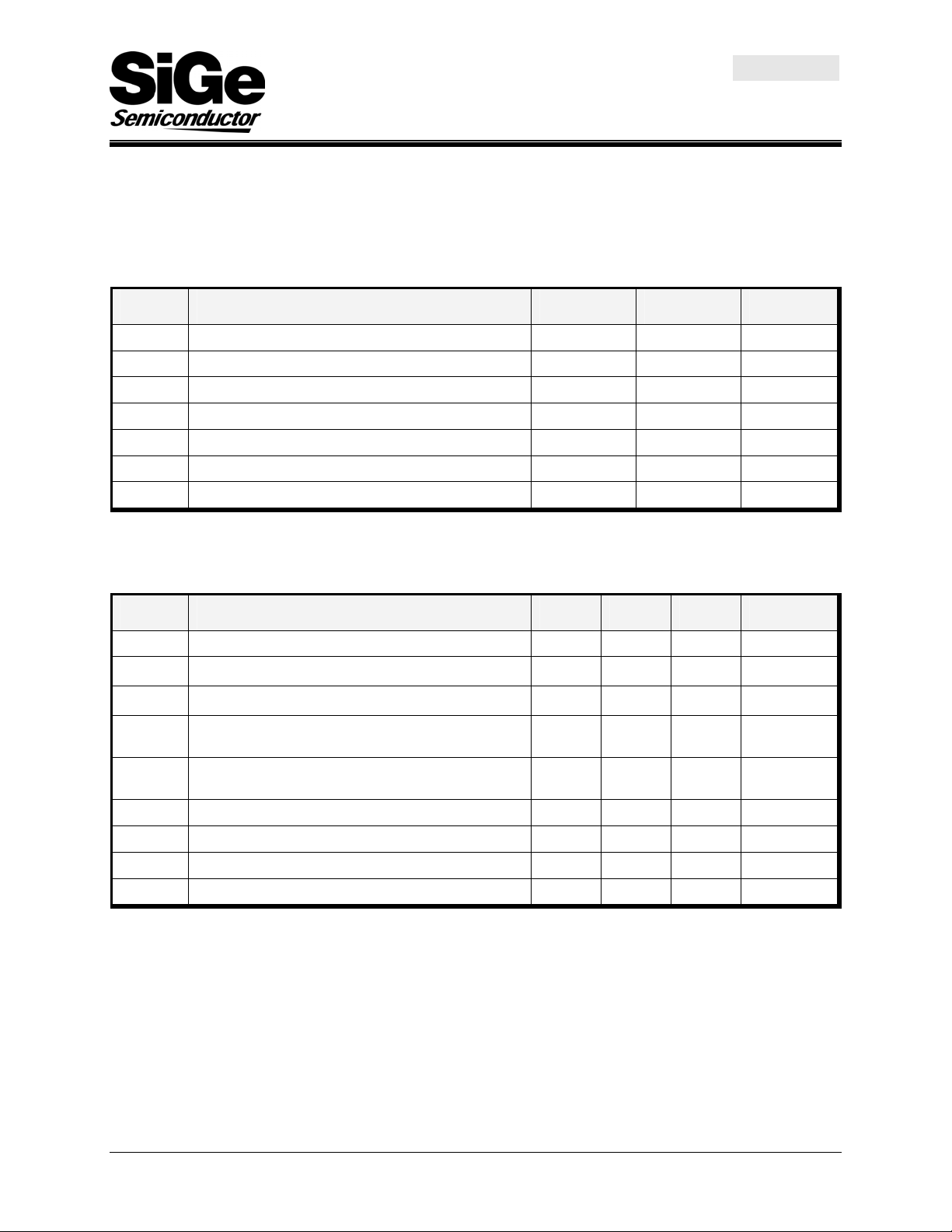
Absolute Maximum Ratings
These are stress ratings only. Exposure to stresses beyond these maximum ratings may cause permanent damage
to, or affect the reliability of the device. Avoid operating the device outside the recommended operating conditions
defined below. This device is ESD sensitive. Handling and assembly of this device should be at ESD protected
workstations.
Symbol Parameter Min. Max. Unit
VCC Supply Voltage on pins V
V
Analog Control Voltage -0.3 VCC V
CTL
CC0, VCC1, VCC2
-0.3 +3.6 V
VEN Ramping Voltage -0.3 VCC V
PIN RF Input Power +8 dBm
TA Operating Temperature Range -40 +85 °C
T
Storage Temperature Range -40 +150 °C
STG
Tj Maximum Junction Temperature +150 °C
DC Electrical Characteristics
Conditions: V
Symbol Parameter Min. Typ. Max. Unit
VCC Supply Voltage 2.7 3.3 3.6 V
I
CC-1DB
I
CC-SAT
∆Icc
TEMP
V
CTL
I
V
CTL
V
Logic High Voltage 1.0 V
ENH
V
Logic Low Voltage 0.5 V
ENL
I
Leakage Current when VEN = 0V. 1 10 µA
OFF
= VEN = 3.3V, V
CC
Supply Current at P
Supply Current at P
Supply Current variation over temperature from
TA = 25°C (-40°C < TA < +85°C)
≥ 1.6V, TA = 25°C, unless otherwise noted.
CTL
1DBH
, VCC = 3.3V
SAT
Recommended PA Gain and Bias Control Voltage
Range
current requirement 275 µA
CTL
250 mA
325 mA
25 %
0.1 1.6 V
61-DST-01 Rev 1.4 Dec 03/02 3 of 8
Page 4
SE2522BL
RangeCharger™ 2.4GHz +23 dBm Power Amplifier
Preliminary Information
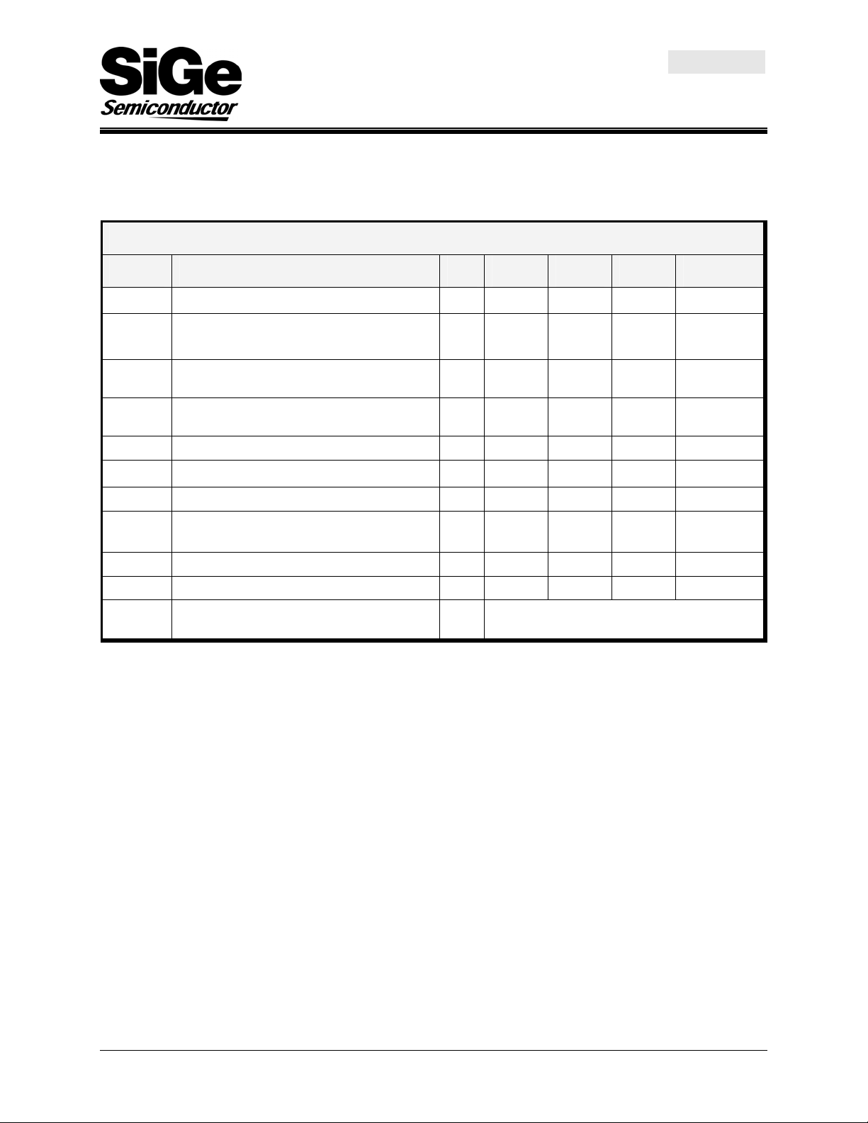
AC Electrical Characteristics
Conditions: V
Symbol Parameter Note Min. Typ. Max. Unit
f
L-U
P
1dBH
P
1dBL
P
SAT
G Small Signal Gain 35 dB
G
VAR
2f,3f,4f,5f Harmonics 3 < -30 dBm/100kHz
S21
OFF
S12 Reverse Gain -42 -32 dB
TR Rise and Fall Time 4 1.2 µs
STAB Stability (PIN ≤ 0dBm, Load VSWR = 6:1)
Notes: (1) Matching networks optimized for linear output power performance.
(2) With matching networks optimized for saturated output power performance.
(3) Harmonic levels and ACPR are greatly affected by topology of external matching networks.
(4) Rise and Fall Time is defined between 10% and 90% final output power level.
= V
CC
= 3.3V, V
EN
≥ 1.6V, P
CTL
< -8dBm, TA = 25°C, f = 2.45 GHz, input and output externally
IN
matched to 50Ω, unless otherwise noted.
Power Amplifier
Frequency Range 2400 2485 MHz
High Gain 1dB Compressed Output Power,
≥ 1.6V
V
CTL
Low Gain 1dB Compressed Output Power,
= 0.1V
V
CTL
Saturated Output Power, P
V
CTL
≥ 1.6V, V
CC
= .3V
= 0dBm,
IN
1 21.0 23 25.0 dBm
1 -5 dBm
2 25 dBm
Gain Variation over band (2400-2485 MHz) 1.0 2.0 dB
Forward Gain when PA is “OFF” State,
P
≤ 0dBm, VEN = 0V
IN
-30 dB
All non-harmonically related outputs less than
-50 dBc/100kHz
61-DST-01 Rev 1.4 Dec 03/02 4 of 8
Page 5
SE2522BL
RangeCharger™ 2.4GHz +23 dBm Power Amplifier
Preliminary Information
Conditions: V
= 3.3V, f = 2.4-2.5Ghz, TA = 25°C, PA Output externally matched to 50Ω, unless otherwise noted.
CC
Power Detector
Symbol Parameter Note Min. Typ. Max. Unit
PDR Power detect range, peak power 6 25 dBm
PDT PA power detect, response time, 5pF load 0.1 0.8 µsec
PDS PA power detect, slope, 10 to 23dBm peak. 1,2 12 14 17 dB/V
PDV
PDV
PDV
PDVA
PA power detect, output voltage maximum,
max
load > 5kΩ
PA power detect, output voltage minimum,
min
load > 5kΩ
PA power detect output voltage,
p23
P
= 23dBm peak
OUT
PA power detect output voltage accuracy,
p23
P
OUT
= 23dBm
1,2 1.7 V
1,2 0.1 V
4 1.1 V
±35 mV
Notes: (1) Matching networks optimized for linear output power performance.
(2) PD response is dependant on PA output matching, above specifications are valid for SiGe
recommended matching networks.
61-DST-01 Rev 1.4 Dec 03/02 5 of 8
Page 6
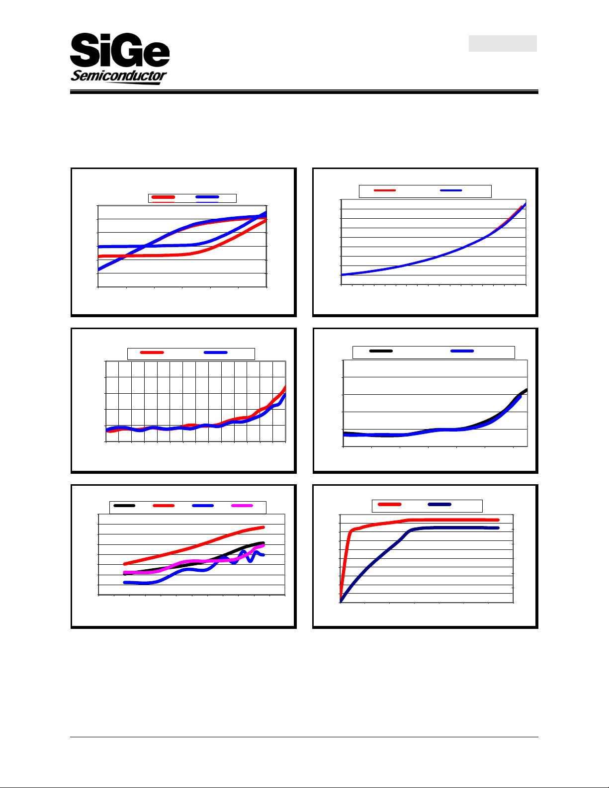
Typical Performance Characteristics
Conditions: V
30
25
20
15
(dBm)
OUT
P
10
5
0
-30 -25 -20 -15 -10 -5 0
-15.00
-20.00
-25.00
-30.00
ACPR (dBc)
-35.00
-40.00
10 11 12 13 14 15 16 17 18 19 20 21 22 23 24
0
-10
-20
-30
-40
-50
Harmonics (dBm/1MHz RBW)
-60
-70
-80
15 16 17 18 19 20 21 22 23 24 25 26 27
Note: Data is without harmonic filter
= 3.3V, V
CC
= 1.6V, V
CTL
= 3.3V, F = 2.45GHz, PIN = -12dBm, using IEEE802.11b modulation, and
EN
matching networks optimized for linear output power performance. Performance graphs are based on
preliminary evaluation information and may differ from the AC and DC electrical specifications.
Output Power an d Supply Current vs. In put Power
4H
3.6V
3.6V
5H
3.3V
Input Power (dBm)
ACPR vs. Output Power
3.3V
Output Power (dBm)
Harmonics vs Output Power
2H
3H
Output Po wer (dBm)
SE2522BL
RangeCharger™ 2.4GHz +23 dBm Power Amplifier
Preliminary Information
V
vs. Output Power
350
320
290
260
(mA)
CC
I
230
200
170
1.8
1.6
1.4
1.2
1.0
(V)
0.8
DET
V
0.6
0.4
0.2
0.0
9 1011121314151617 181920212223242526
-15
-20
-25
-30
ACPR (dBc)
-35
-40
11 13 15 17 19 21 23
30
20
10
0
-10
-20
(dBm)
OUT
-30
P
-40
-50
-60
-70
0.0 0.5 1.0 1.5 2.0 2. 5 3.0 3.5
DET
3.3V
Output Power (dBm)
ACPR Across the Frequency Band
3.6V
2.4GHz 2.5GHz
Output Power (dBm)
Power Control Profile, PIN = -8dBm
Pout
V
CTL
Icc (mA)
(V)
300
250
200
150
100
50
0
(mA)
CC
I
61-DST-01 Rev 1.4 Dec 03/02 6 of 8
Page 7
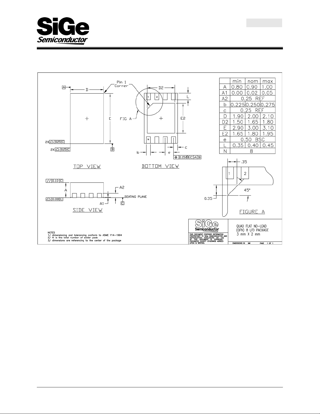
Package Description
SE2522BL
RangeCharger™ 2.4GHz +23 dBm Power Amplifier
Preliminary Information
61-DST-01 Rev 1.4 Dec 03/02 7 of 8
Page 8

SE2522BL
RangeCharger™ 2.4GHz +23 dBm Power Amplifier
Preliminary Information
http://www.sige.com
Headquarters: Canada
Phone: +1 613 820 9244
Fax: +1 613 820 4933
2680 Queensview Drive
Ottawa ON K2B 8J9 Canada
San Diego United Kingdom
Phone: +1 858 668 3541 South Building, Walden Court
Fax: +1 858 668 3546 Parsonage Lane, Bishop’s Stortford
Hertfordshire CM23 5DB
Hong Kong
Phone: +44 1279 464 200
Phone: +852 2491 8637 Fax: +44 1279 464 201
Fax: +852 2491 8937
Product Preview
The datasheet contains information from the product concept specification. SiGe Semiconductor Inc. reserves the right to change
information at any time without notification.
Preliminary Information
The datasheet contains information from the design target specification. SiGe Semiconductor Inc. reserves the right to change
information at any time without notification.
Final
The datasheet contains information from the final product specification. SiGe Semiconductor Inc. reserves the right to change
information at any time without notification. Production testing may not include testing of all parameters.
Information furnished is believed to be accurate and reliable and is provided on an “as is” basis. SiGe Semiconductor Inc. assumes
no responsibility or liability for the direct or indirect consequences of use of such information nor for any infringement of patents or
other rights of third parties, which may result from its use. No license or indemnity is granted by implication or otherwise under any
patent or other intellectual property rights of SiGe Semiconductor Inc. or third parties. Specifications mentioned in this publication
are subject to change without notice. This publication supersedes and replaces all information previously supplied. SiGe
Semiconductor Inc. products are NOT authorized for use in implantation or life support applications or systems without express
written approval from SiGe Semiconductor Inc.
RangerCharger
Copyright 2002 SiGe Semiconductor
All Rights Reserved
TM
, StreamChargerTM, PointChargerTM, and LightChargerTM are trademarks owned by SiGe Semiconductor Inc.
61-DST-01 Rev 1.4 Dec 03/02 8 of 8
 Loading...