

Page 1

© 2017 ROHM Co., Ltd.
No. 60AP001E Rev.001
2017.4
© 2016 ROHM Co., Ltd.
No. 60UG018E Rev.002
APR.2017
User’s Guide
Parameter
Min
Typ
Max
Units
Conditions
Input Voltage Range
7.0 36
V
Output Voltage
5.0 V
R1=30kΩ, R2=7.5kΩ
Output Voltage Setting Range
VIN×0.06
VIN×0.8
V
Output Current Range
0 3
A
Loop Band Width
18.2 kHz
Phase Margin
70.8
degrees
Input Ripple Voltage
300 mVpp
IO = 3A
Output Ripple Voltage
30 mVpp
IO = 3A
Output Rising Time
2.2 ms
Operating Frequency
300 kHz
Maximum Efficiency
91.1 %
IO = 1.2A
(NOTE1)
Switching Regulator Series
Step-Down DC/DC Converter
BD9E303EFJ-LB Evaluation Board
BD9E303EFJ-EVK-001
BD9E303EFJ-EVK-001 Evaluation board delivers an output 5.0 volts from an input 7.0 to 36 volts using BD9E303EFJ-LB, a synchronous rectification
step-down DC/DC converter integrated circuit, with output current rating of maximum 3A. The output voltage can be set by changing the external
parts of circuit and the loop-response characteristics also can be adjusted by the phase compensation circuit.
Performance specification
These are representative values, and it is not a guaranteed against the characteristics.
VIN = 24V, V
= 5.0V, Unless otherwise specified.
OUT
(NOTE1) However, (VIN×0.06) ≥ 1.0V
1/10
Page 2
User’s Guide
BD9E303EFJ-EVK-001
© 2016 ROHM Co., Ltd.
No. 60UG018E Rev.002
APR.2017
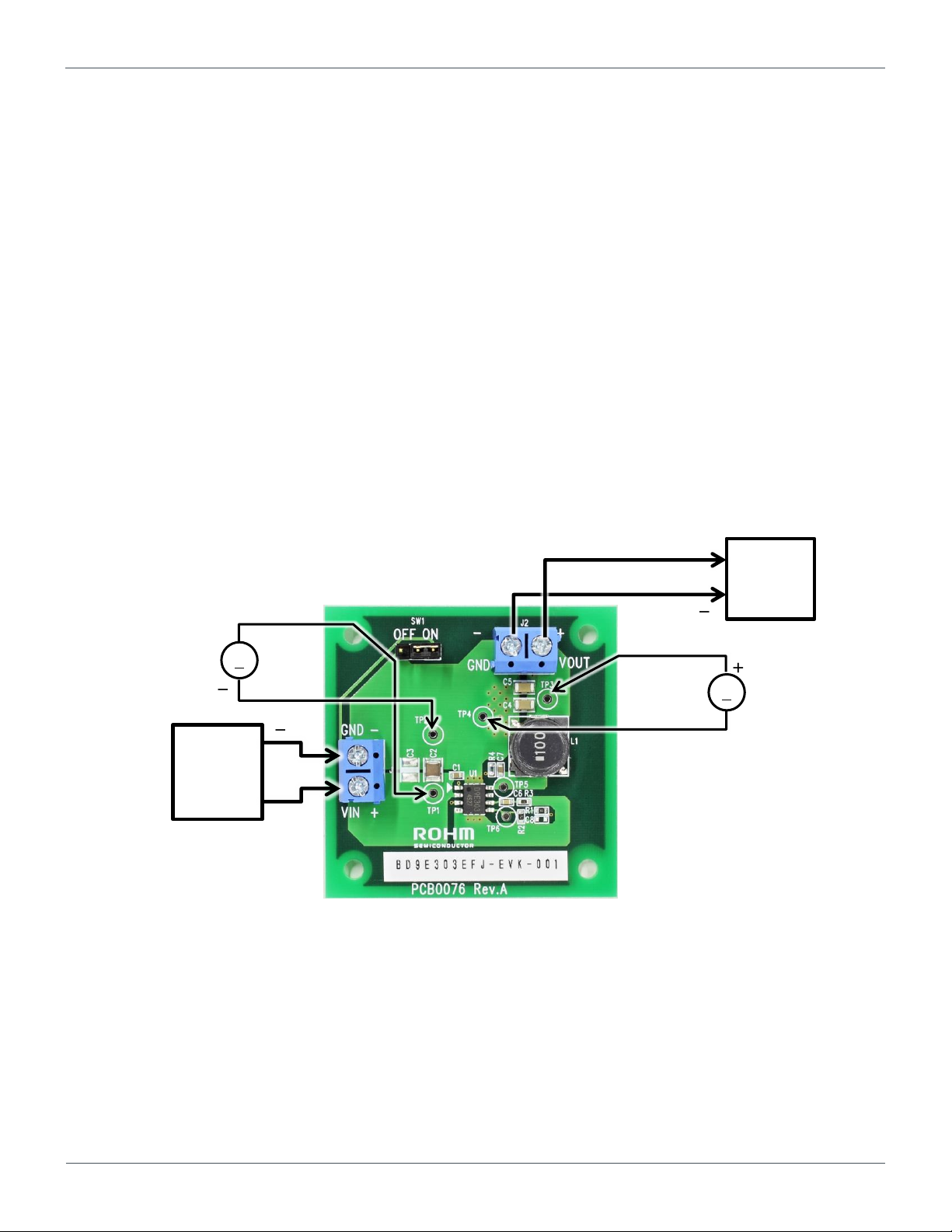
DC Voltmeter 1
DC Voltmeter 2
+
-
+
V
V
+
DC Power
Load
Operation Procedures
1. Necessary equipments
(1) DC power-supply of 7.0V to 36V/3A
(2) Maximum 3A load
(3) DC voltmeter
2. Connecting the equipments
(1) DC power-supply presets to 24V and then the power output turns off.
(2) The maximum load should be set at 3A and over it will be disabled.
(3) Check Jumper pin of SW1 is short, between intermediate-terminal and OFF-side terminal.
(4) Connect positive-terminal of power-supply to VIN+ terminal and negative-terminal to GND-terminal with a pair of wires.
(5) Connect load’s positive-terminal to VOUT+ terminal and negative-terminal to GND-terminal with a pair of wires.
(6) Connect positive-terminal of DC voltmeter 1 to TP1 and negative-terminal to TP2 for input-voltage measurement.
(7) Connect positive-terminal of DC voltmeter 2 to TP3 and negative-terminal to TP4 for output-voltage measurement.
(8) DC power-supply output is turned ON.
(9) IC is enable (EN) by shorting Jumper-pin of SW1 between intermediate-terminal and ON-side terminal.
(10) Check DC voltmeter 2 displays 5.0V.
(11) The load is enabled.
(12) Check at DC voltmeter 1 whether the voltage-drop (loss) is not caused by the wire’s resistance.
Figure 1. Connection Diagram
Enable-Pin
To minimize current consumption during standby-mode and normal operation, Enable-mode can be switched by controlling EN pin
(3pin) of the IC. Standby-mode is enabled by shorting Jumper-pin of SW1 between intermediate-terminal and OFF-side terminal
and normal-mode operation by shorting between intermediate-terminal and ON-side terminal.
It also can be switched between standby-mode and normal-mode operation by removing Jumper-pin and controlling the voltage
between EN and GND-terminal. Standby-mode is enabled when the voltage of EN is under 0.8V, and normal-mode operation when
it is over 2.5V.
2/10
Page 3
User’s Guide
BD9E303EFJ-EVK-001
© 2016 ROHM Co., Ltd.
No. 60UG018E Rev.002
APR.2017
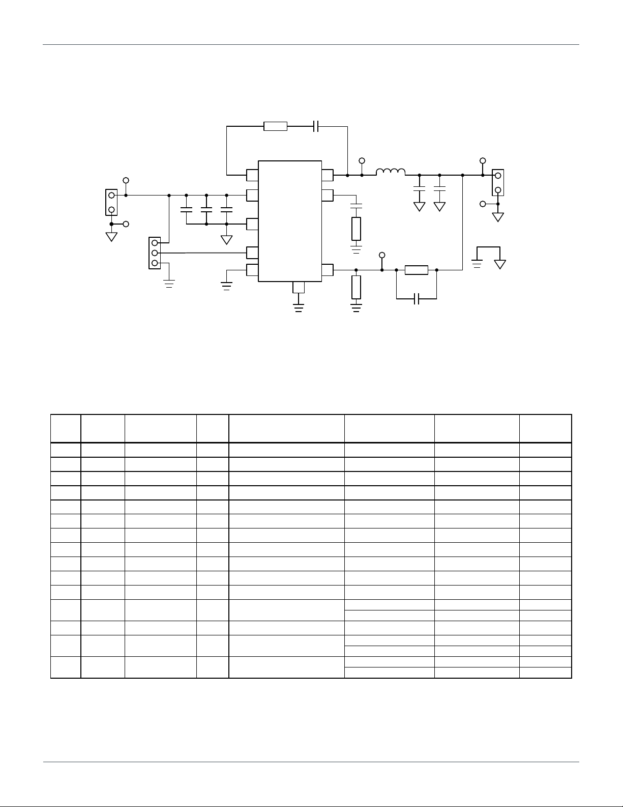
1 BOOT
2 VIN
7 PGND
3 EN
4 AGND
SW 8
COMP 6
FB 5
U1
BD9E303EFJ-LB
C7
C2
L1
C4
C6
R3
R1
R2
VIN
VOUT
C5
C1
C8
R4
C3
SW1
ON
OFF
GND
J1
TP1
TP2
J2
TP3
TP4
GND
TP5
TP6
9 E-PAD
2 C1, C7 Ceramic Capacitor
0.1µF 50V, B, ±20% GRM188B31H104MA92 MURATA 1608
1 C2 Ceramic Capacitor
10µF 50V, B, ±10% GRM32EB31H106KA12 MURATA 3225
0 C3 Ceramic Capacitor -
Not installed - - 3225
2 C4, C5 Ceramic Capacitor
22µF 10V, B, ±10% GRM31CB31A226KE19 MURATA 3216
1 C6 Ceramic Capacitor
6800pF 50V, B, ±10% GRM188B11H682KA01 MURATA 1608
0 C8 Ceramic Capacitor
- Not installed - - 1608
1 L1 Inductor
10µH ±20%, DCR=24mΩmax, 4.49A NS10155T100MNV TAIYO YUDEN 101101
1 R1 Resistor
30kΩ 1/10W, 50V, 1% MCR03EZPFX3002 ROHM 1608
1 R2 Resistor
7.5kΩ 1/10W, 50V, 1% MCR03EZPFX7501 ROHM 1608
1 R3 Resistor
15kΩ 1/10W, 50V, 1% MCR03EZPFX1502 ROHM 1608
1 R4 Resistor
0Ω Jumper MCR03EZPJ000 ROHM 1608
PH-1x03SG USECONN 61300311121 Wurth Electronics Inc. -
1 U1 IC
- Buck DC/DC Converter BD9E303EFJ-LB ROHM HTSOP-J8
TB111-2-2-U-1-1
Alphaplus Connectors & Cables
-
OSTTC022162
On Shore Technology Inc
MJ254-6BK USECONN 969102-0000-DA 3M -
1-Jumper
-
Jumper pin for SW1
2
J1, J2
Terminal Block
-
2 contacts, 15A, 14 to 22AWG
1
SW1
Pin header
-
2.54mm × 3 contacts
Reference
Designator
Count
Manufacturer
Part Number
Manufacturer
Configuration
(mm)
Type
Value
Description
Circuit Diagram
VIN = 7.2V to 36V, V
OUT
= 5.0V
Figure 2. BD9E303EFJ-EVK-001 Circuit Diagram
Bill of Materials
3/10
Page 4
User’s Guide
BD9E303EFJ-EVK-001
© 2016 ROHM Co., Ltd.
No. 60UG018E Rev.002
APR.2017
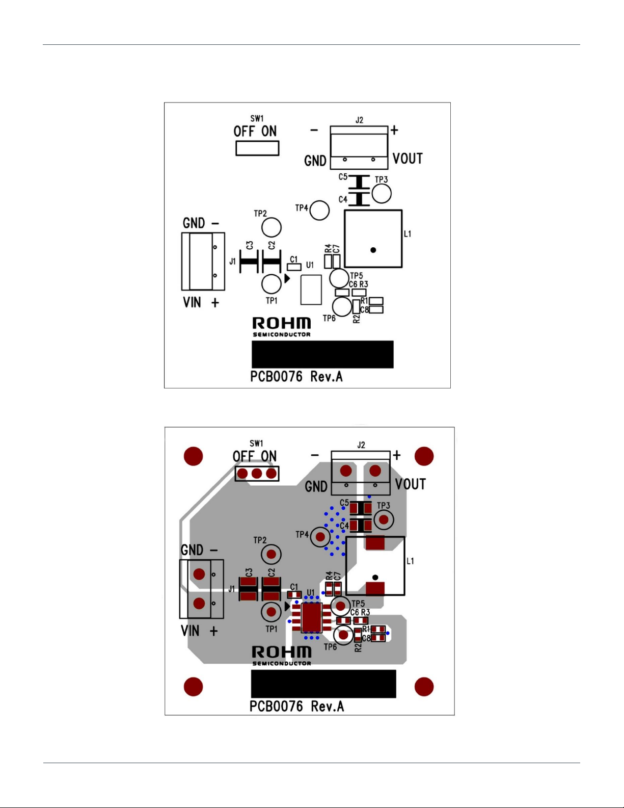
Layout
PCB size: 50mm×50mm×1.6mm
Figure 3. Top Silk Screen (Top view)
Figure 4. Top Silk Screen and Layout (Top view)
4/10
Page 5

User’s Guide
BD9E303EFJ-EVK-001
© 2016 ROHM Co., Ltd.
No. 60UG018E Rev.002
APR.2017
Figure 5. Top Side Layout (Top view)
Figure 6. L2 Layout (Top view)
5/10
Page 6

User’s Guide
BD9E303EFJ-EVK-001
© 2016 ROHM Co., Ltd.
No. 60UG018E Rev.002
APR.2017
Figure 7. L3 Layout (Top view)
Figure 8. Bottom Side Layout (Top view)
6/10
Page 7

User’s Guide
BD9E303EFJ-EVK-001
© 2016 ROHM Co., Ltd.
No. 60UG018E Rev.002
APR.2017
50
60
70
80
90
100
0 1 2 3
Efficiency (%)
Load Current (A)
VIN=7V
VIN=24V
VO=5.0V
VIN=36V
VIN=12V
-1
-0.8
-0.6
-0.4
-0.2
0
0.2
0.4
0.6
0.8
1
5 10 15 20 25 30 35 40
Output Voltage Change (%)
Input Voltage (V)
IO=1.0A
-0.5
-0.4
-0.3
-0.2
-0.1
0
0.1
0.2
0.3
0.4
0.5
0 0.5 1 1.5 2 2.5 3
Output Voltage Change (%)
Load Current (A)
VIN=12V
VIN=24V
VO=5.0V
Figure 9. Efficiency vs Load Current
Figure 10. Line Regulation
Figure 11. Load Regulation
Figure 12. Load Transient Characteristics
VO (AC)
200mV/div
IO: 1A/div
IO: 1A/div
Time scale 1ms/div
V
IN
= 12V
VO = 5.0V
V
IN
= 24V
VO = 5.0V
IO: 1A→3A→1A
IO: 1A→3A→1A
VO (AC)
200mV/div
Time scale 1ms/div
Reference Application Data
7/10
Page 8

User’s Guide
BD9E303EFJ-EVK-001
© 2016 ROHM Co., Ltd.
No. 60UG018E Rev.002
APR.2017
Figure 13. Loop Response VIN = 12V, VO = 5.0V, IO = 3A
Frequency (Hz)
Frequency (Hz)
Gain (dB)
Gain (dB)
Phase (deg)
Phase (deg)
Phase
Phase
Gain
Gain
fC = 16.6kHz
Phase margin = 63.5deg
Gain margin = 25.1dB
fC = 18.2kHz
Phase margin = 70.8deg
Gain margin = 22.8dB
Figure 14. Loop Response VIN = 24V, VO = 5.0V, IO = 3A
8/10
Page 9
User’s Guide
BD9E303EFJ-EVK-001
© 2016 ROHM Co., Ltd.
No. 60UG018E Rev.002
APR.2017
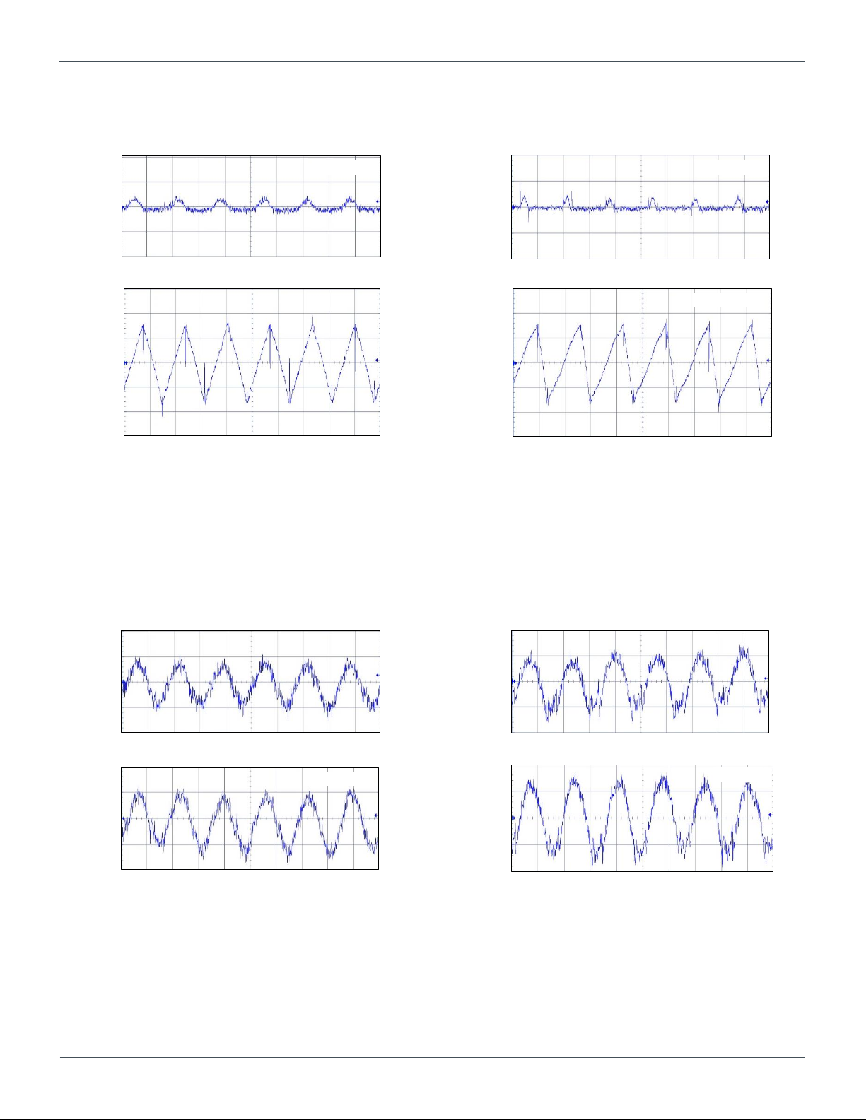
Figure 15. Input Voltage Ripple Wave
VIN = 12V, VO = 5.0V
V
IN
(AC)
50mV/div
Time scale 2μs/div
Time scale 2μs/div
V
IN
(AC)
100mV/div
Figure 16. Input Voltage Ripple Wave
VIN = 24V, VO = 5.0V
IO = 0A
IO = 3A
V
IN
(AC)
50mV/div
V
IN
(AC)
100mV/div
IO = 0A
IO = 3A
Time scale 2μs/div
Time scale 2μs/div
Time scale 2μs/div
Time scale 2μs/div
IO = 0A
IO = 3A
VO (AC)
10mV/div
VO (AC)
10mV/div
Figure 17. Output Voltage Ripple Wave
VIN = 12V, VO = 5.0V
Figure 18. Output Voltage Ripple Wave
VIN = 24V, VO = 5.0V
Time scale 2μs/div
Time scale 2μs/div
IO = 0A
IO = 3A
VO (AC)
10mV/div
VO (AC)
10mV/div
9/10
Page 10

User’s Guide
BD9E303EFJ-EVK-001
© 2016 ROHM Co., Ltd.
No. 60UG018E Rev.002
APR.2017
Figure 19. Start-up EN = VIN
VIN = 12V, VO = 5.0V, IO = 0A
V
IN
5V/div
EN
5V/div
VO
2V/div
Time scale 100ms/div
Time scale 100ms/div
Figure 20. Power-down EN = VIN
VIN = 12V, VO = 5.0V, IO = 0A
V
IN
10V/div
EN
10V/div
VO
2V/div
Time scale 100ms/div
Time scale 100ms/div
Figure 21. Start-up EN = VIN
VIN = 24V, VO = 5.0V, IO = 0A
Figure 22. Power-down EN = VIN
VIN = 24V, VO = 5.0V, IO = 0A
V
IN
5V/div
EN
5V/div
VO
2V/div
Time scale 1ms/div
Time scale 1s/div
Figure 23. Start-up by EN
VIN = 12V, VO = 5.0V, IO = 0A
Figure 24. Power-down by EN
VIN = 12V, VO = 5.0V, IO = 0A
V
IN
10V/div
EN
10V/div
VO
2V/div
Time scale 1ms/div
Time scale 1s/div
Figure 25. Start-up by EN
VIN = 24V, VO = 5.0V, IO = 0A
Figure 26. Power-down by EN
VIN = 24V, VO = 5.0V, IO = 0A
10/10
Page 11

Notes
The information contained herein is subject to change without notice.
1)
Before you use our Products, please contact our sales representative and verify the latest specifica-
2)
tions :
Although ROHM is continuously working to improve product reliability and quality, semicon-
3)
ductors can break down and malfunction due to various factors.
Therefore, in order to prevent personal injury or fire arising from failure, please take safety
measures such as complying with the derating characteristics, implementing redundant and
fire prevention designs, and utilizing backups and fail-safe procedures. ROHM shall have no
responsibility for any damages arising out of the use of our Poducts beyond the rating specified by
ROHM.
Examples of application circuits, circuit constants and any other information contained herein are
4)
provided only to illustrate the standard usage and operations of the Products. The peripheral
conditions must be taken into account when designing circuits for mass production.
The technical information specified herein is intended only to show the typical functions of and
5)
examples of application circuits for the Products. ROHM does not grant you, explicitly or implicitly,
any license to use or exercise intellectual property or other rights held by ROHM or any other
parties. ROHM shall have no responsibility whatsoever for any dispute arising out of the use of
such technical information.
Notice
The Products specified in this document are not designed to be radiation tolerant.
6)
For use of our Products in applications requiring a high degree of reliability (as exemplified
7)
below), please contact and consult with a ROHM representative : transportation equipment (i.e.
cars, ships, trains), primary communication equipment, traffic lights, fire/crime prevention, safety
equipment, medical systems, servers, solar cells, and power transmission systems.
Do not use our Products in applications requiring extremely high reliability, such as aerospace
8)
equipment, nuclear power control systems, and submarine repeaters.
ROHM shall have no responsibility for any damages or injury arising from non-compliance with
9)
the recommended usage conditions and specifications contained herein.
ROHM has used reasonable care to ensure the accuracy of the information contained in this
10)
document. However, ROHM does not warrants that such information is error-free, and ROHM
shall have no responsibility for any damages arising from any inaccuracy or misprint of such
information.
Please use the Products in accordance with any applicable environmental laws and regulations,
11)
such as the RoHS Directive. For more details, including RoHS compatibility, please contact a
ROHM sales office. ROHM shall have no responsibility for any damages or losses resulting
non-compliance with any applicable laws or regulations.
When providing our Products and technologies contained in this document to other countries,
12)
you must abide by the procedures and provisions stipulated in all applicable export laws and
regulations, including without limitation the US Export Administration Regulations and the Foreign
Exchange and Foreign Trade Act.
This document, in part or in whole, may not be reprinted or reproduced without prior consent of
13)
ROHM.
Thank you for your accessing to ROHM product informations.
More detail product informations and catalogs are available, please contact us.
ROHM Customer Support System
www.rohm.com
© 2016 ROHM Co., Ltd. All rights reserved.
http://www.rohm.com/contact/
R1102
B
 Loading...