ROHM BR93LC46RFJ-W, BR93LC46RF-W, BR93LC46FV-W, BR93LC46FJ-W Datasheet

BR93LC46-W / BR93LC46F-W / BR93LC46RF-W /
Memory ICs
BR93LC46FJ-W / BR93LC46RFJ-W / BR93LC46FV-W
64×16bits serial EEPROM
BR93LC46-W / BR93LC46F-W / BR93LC46RF-W /
BR93LC46FJ-W / BR93LC46RFJ-W / BR93LC46FV-W
The BR93LC46-W series are CMOS serial input / output-type memory circuits (EEPROMs) that can be programmed
electrically. Each is configured of 64 words × 16 bits (1,024 bits), and each word can be accessed individually and data
read from it and written to it. Operation control is performed using five types of commands.
The commands, addresses, and data are input through the DI pin under the control of the CS and SK pins. In a write
operation, the inter nal stat us si gnal (READ Y or BUSY) can be o utput fro m th e DO pin.
z
zApplications
zz
VCRs, TVs, printers, car stereos, cordless telephones, short wave radios, programmable DIP switches, and
other battery-powered equipment requiring low voltage and low current
z
zFeatures
zz
1) 64 words × 16 bits EEPROM
2) Operati ng v oltag e ran ge
When reading : 2.0 to 5.5V
When writing : 2.7 to 5.5V
3) Low current consumption
Operating (at 5V) : 3mA (Max .)
Standby (at 5V) : 5µA (M ax.)
4) Address can be incremented automatically during
read operations.
5) Auto erase and auto complete functions can be used
during write operations.
6) A write instru ction i nhibit function allow s :
- write protection when power supply voltage is low.
- write disable state at power up.
- writing using command codes.
7) Compact packages
8) Display of READY / BUSY stat us
9) TTL-compatible input / output
10) Rewriting possible up to 100,000 times
11) Data can be stored for ten years without corruption.
zzzz
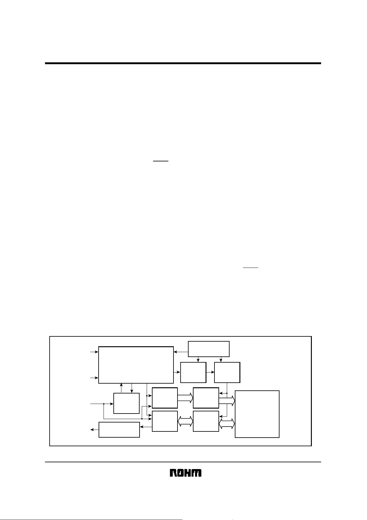
Block diagram
DO
Power supply
CS
SK
DI
Command decode
Control
Clock generation
Command
register
Dummy bits
Address
buffer
Data
register
6bits
16bits
voltage detector
Write
disable
Address
decoder
R / W
amplifier
High voltage
generator
6bits
1,024bits
EEPROM array
16bits

Memory ICs
z
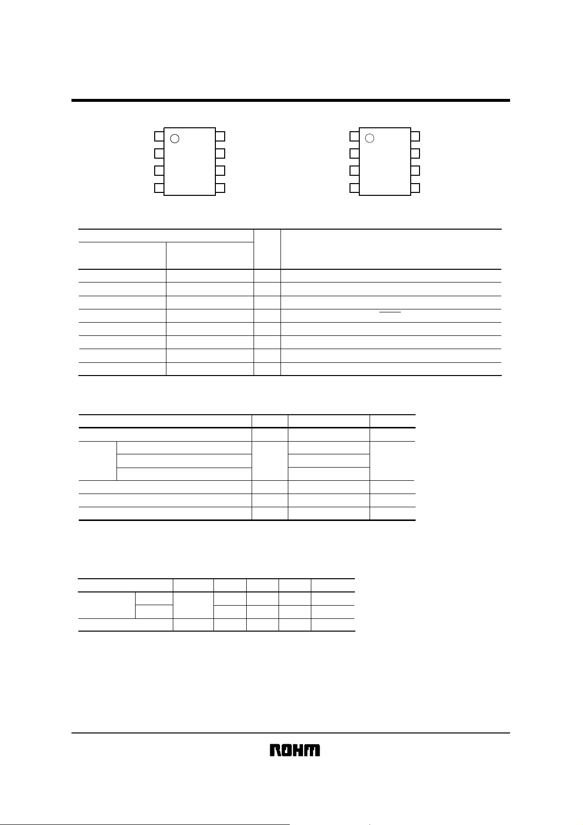
zPin descriptions
zz
BR93LC46-W / BR93LC46F-W / BR93LC46RF-W /
BR93LC46FJ-W / BR93LC46RFJ-W / BR93LC46FV-W
CS
1
SK
2
BR93LC46-W
V
8
N.C.
7
BR93LC46RF-W
BR93LC46RFJ-W
DI
DO
3
4
Fig.1
6
N.C.
5
GND
Pin No.
BR93LC46-W
BR93LC46RF-W
BR93LC46RFJ-W
BR93LC46F-W
BR93LC46FJ-W
BR93LC46FV-W
13CS
24SK
35DI
46DO
5 7 GND
6 8 N.C.
7 1 N.C.
82V
zzzz
Absolute maximum ratings
(T a = 2 5°C)
Parameter
Applied voltage
BR93LC46-W
Power
dissipation
BR93LC46FV-W
Storage temperature
Operating temperature
Terminal voltage
∗1 Reduced by 5.0mW for each increase in Ta of 1°C over 25°C.
∗2 Reduced by 3.5mW for each increase in Ta of 1°C over 25°C.
∗3 Reduced by 3.0mW for each increase in Ta of 1°C over 25°C.
CC
N.C.
V
1
CC
2
BR93LC46F-W
N.C.
8
GND
7
BR93LC46FJ-W
BR93LC46FV-W
Pin
name
3
CS
4
SK
Fig.2
Function
6
DO
5
DI
Chip select input
Serial clock input
Start bit, operating code, address, and seria data input
Serial data output, READY / BUSY internal status display output
Ground
Not connected
Not connected
CC
Power supply
Symbol
V
CC
Pd
Tstg
Topr
−
Limits Unit
−0.3~+6.5
∗1
500
∗2
∗3
300
~+
125
−65
~+
85
−40
~
V
CC
+
−0.3
0.3
V
mWBR93LC46F-W / RF-W / FJ-W / RFJ-W 350
°C
°C
V
z
zRecommended operating conditions (T a = 25°C)
zz
Parameter Symbol Min. Typ. Max. Unit
Power supply
voltage
Input voltage
Writing
Reading
V
CC
V
IN
2.7
2.0 − 5.5 V
0 − V
− 5.5 V
CC
V

BR93LC46-W / BR93LC46F-W / BR93LC46RF-W /
Memory ICs
z
zElectrical characteristics
zz
For 5V operation (unless otherwise noted, Ta = −40 to + 85°C, V
Parameter
Input low level voltage
Input high level voltage
Output low level voltage 1
Output high level voltage 1
Output low level voltage 2
Output high level voltage 2
Input leakage current
Output leakage current
Operating current
dissipation 1
Operating current
dissipation 2
Standby current
For 3V operation (unless otherwise noted, Ta = −40 to + 85°C, VCC = 3.0V ± 10%)
Parameter Symbol Min. Typ. Max. Unit Conditions
Input low level voltage
Input high level voltage
Output low level voltage
Output high level voltage
Input leakage current
Output leakage current
Operating current
dissipation 1
Operating current
dissipation 2
Standby current
BR93LC46FJ-W / BR93LC46RFJ-W / BR93LC46FV-W
= 5.0V ± 10%)
CC
Symbol Min. Typ. Max. Unit Conditions
V
IL
−0.3 −
IH
V
V
V
V
V
I
I
I
CC1
I
CC2
I
V
IL
V
IH
OL
V
V
OH
I
LI
I
LO
I
CC1
CC2
I
I
SB
2.0
OL1
OH1
OL2
OH2
LI
LO
SB
−−
2.4
−−
VCC−0.4 −
−1.0 −µAVIN=0V~V
−1.0 −µAV
1.5 3.0 mA
−
0.7 1.5 mA
−
1.0 5.0
−
−0.3 −
0.7×V
CC
−
−−0.2 V IOL=10µA
VCC−0.4 −−VIOH=−10µA
−1.0 −µAVIN=0V~V
−1.0 −µA
− 0.5 2.0 mA
− 0.2 1.0 mA
0.4 3.0
−
0.8 V
−−
V
CC
0.4 V
−−
0.2 V
− V
V
+
0.3
IOL=2.1mA
V
OH
=−0.4mA
I
IOL=10µA
IOH=−10µA
1.0
1.0
OUT
=0V~VCC, CS=GND
VIN=VIH / VIL, DO=OPEN,
f=1MHz, WRITE
V
IN=VIH
/ VIL, DO=OPEN,
f=1MHz, READ
µACS=SK=DI=GND, DO=OPEN
0.15×V
CC
V
CC
+
0.3 V
1.0
1.0
OUT
=0V~VCC, CS=GND
V
V
IN=VIH
/ VIL, DO=OPEN
f=250kHz, WRITE
V
IN=VIH
/ VIL, DO=OPEN
f=250kHz, READ
µACS=SK=DI=GND, DO=OPEN
Measurement circuit
−
−
−
Fig.3
Fig.4
Fig.3
Fig.4
CC
Fig.5
Fig.6
Fig.7
Fig.7
Fig.8
Measurement circuit
−
−V
−
−
Fig.3
Fig.4
CC
Fig.5
Fig.6
Fig.7
Fig.7
Fig.8
For 2V operation (unless otherwise noted, Ta = −40 to + 85°C, VCC = 2.0V)
Parameter Symbol Min. Typ. Max. Unit Conditions
Input low level voltage
Input high level voltage
Output low level voltage
Output high level voltage
Input leakage current
Output leakage current
Operating current
dissipation 2
Standby current
V
IL
−0.3 −
V
IH
0.7×V
CC
V
OL
V
OH
I
LI
I
LO
I
CC2
SB
I
−−0.2 V IOL=10µA
VCC−0.4 −−VIOH=−10µA
−1.0 −µAVIN=0V~V
−1.0 −µA
− 0.2 1.0 mA
−
0.4
0.15×V
CC
−
CC
+
0.3 V
1.0
1.0
3.0
V
V
V
f=200kHz, READ
µA
CS=SK=DI=GND, DO=OPEN
−
−V
CC
OUT
=0V~VCC, CS=GND
IN=VIH
/ VIL, DO=OPEN
Measurement circuit
−
−
Fig.3
Fig.4
Fig.5
Fig.6
Fig.7
Fig.8

Memory ICs
z
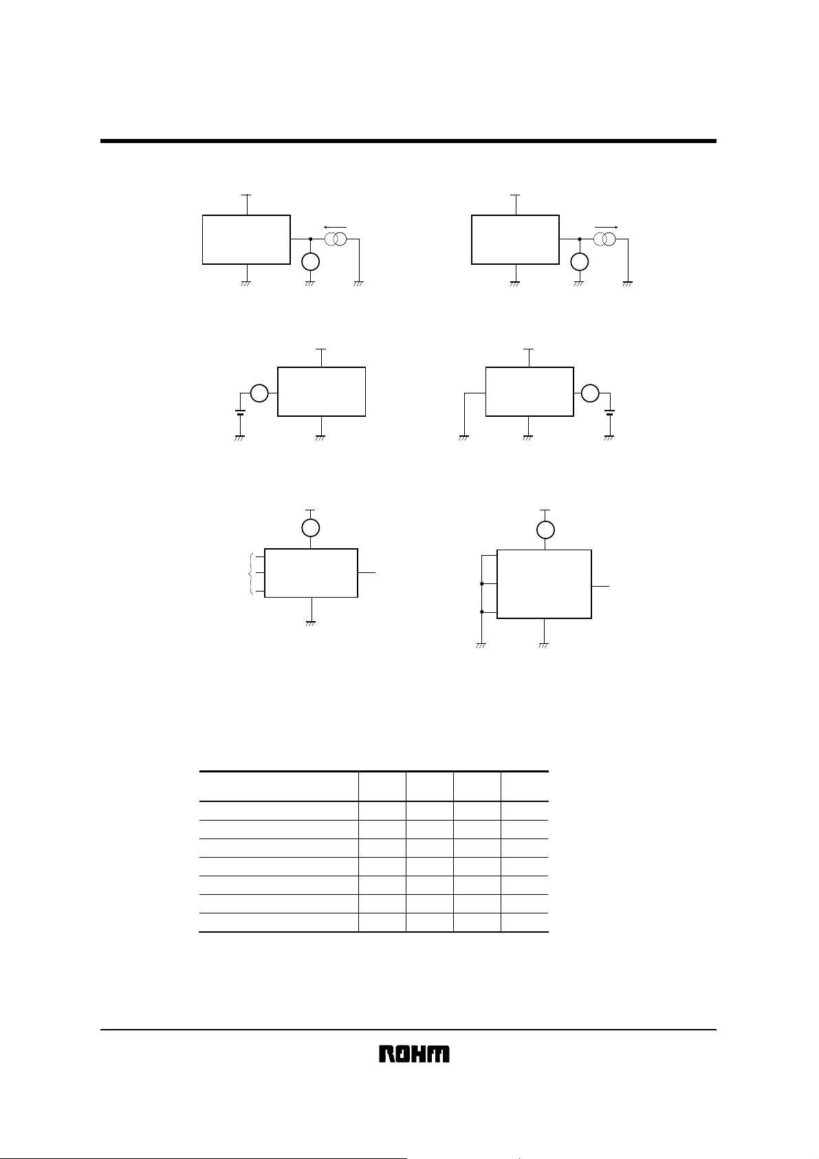
zMeasurement circuits
zz
BR93LC46-W / BR93LC46F-W / BR93LC46RF-W /
BR93LC46FJ-W / BR93LC46RFJ-W / BR93LC46FV-W
V
V
GND
CC
CC
DO
VV
I
OL
OL
V
V
GND
CC
CC
DO
VV
I
OH
OH
VIN=0~V
SK
=1MHz / 250kHz / 200kHz
f
V
IN=VIH
/ V
IL
WRITE / READ INPUT
CS,SK,DI
CS
SK
DI
Control output to "LOW"
V
CC
A
V
CC
GND
Fig.3 "LOW" output voltage circuit
I
LI
A
CC
Fig.5 Input leak current circuit
Fig.7 Supply current circuit
V
V
GND
CC
CC
I
CC
DO OPEN
Control output to "HIGH"
Fig.4 "HIGH" output voltage circuit
V
CC
V
CC
GND
Fig.6 Output leak current circuit
Vcc
A
Vcc
CS
SK
DI
GND
Fig.8 Standby current circuit
I
LO
DOCS
A
SB
I
DO
OPEN
VO=0~V
CC
zzzz
Circuit operation
(1) Command mode
With these ICs, commands are not recognized or acted upon until the start bit is received. The start bit is taken as
the first “1” that is received after the CS pin rises.
Start
Command
Read (READ)
∗1
Write enabled (WEN)
Write (WRITE)
Write all addresses (WRAL)
∗2
∗2
Write disabled (WDS)
Erase (ERASE)
Chip erase (ERAL)
X: Either VIH or V
∗1 After setting of the read command and input of the SK clock, data corresponding to the specified address is output,
with data corresponding to upper addresses then output in se-quence. (Auto increment function)
∗2 When the write or write all addresses command is executed, all data in the selected memory cell is erased
autematically, and the input data is writen to the cell.
∗3 These modes are optinal modes. Please contact Rohm for information on operation timing.
∗3
∗3
IL
Operating
bit
110
100
1 01 D15
1 00 D15
100
111
100
code
Address Data
A5~A0
11XXXX
−
−
A5~A0
01XXXX
00XXXX
A5~A0
10XXXX
−
−
−
~
D0
~
D0
 Loading...