ROHM BR93C46-10SU-2.7 Technical data

A
Universal Standard Specification Series Serial EEPROM Series
Advantage Series Serial EEPROMs
Microwire BUS
BR93C□□-10□U-2.7 family
●Description
The BR93C46/56/66/76/86 series ICs are serial EEPROMs of 1K/2K/4K/8K/16Kbits, respectively, that feature low voltage
operation and low power consumption, enabling compatibility with a wide range of applications. In addition, compact
packages are available, contributing to end-product miniaturization.
●Features
Microwire Bus interface
Single supply voltage: 2.7 to 5.5V
16bit serial EEPROM
Automatic ERASE before WRITE and self-timed programming cycle
Ready /Busy status
2MHz Clock Frequency, 10ms WRITE Time
Auto-increment of register address for READ mode
1,000,000 WRITE/ERASE Cycles
40-year data retention
●Pin configuration
Table1.Pin Configurations
Pin Name Function
CS Chip Select
SK Serial Data Clock
DI Serial Data Input
DO Serial Data Output
GND Ground
VCC Power Supply
DC Don’t Connect
These EEPROMs utilize a three line serial interface
consisting of Serial Data Input (DI), Serial Clock (SK), and
Serial Data Output (DO)
After one READ instruction segment is received, if the Chip
Select (CS) remains HIGH, the address pointer
automatically cycles to the next higher register address,
giving a continuous string of output data, depending on the
device and the starting address.
When a WRITE or WRAL instruction is received, the
previous data in the address locations are automatically
overwritten, eliminating the need for an ERASE command.
When Chip Select (CS) is set to H after the WRITE
command, the Status signal (Ready/Busy) becomes active
at the Serial Data Output (DO) until the start bit of the next
command. The Status signal is active when Chip Select (CS)
is HIGH, and Serial Data Output (DO) pin outputs High – Z
when Chip Select (CS) is LOW.
CS
SK
DI
DO
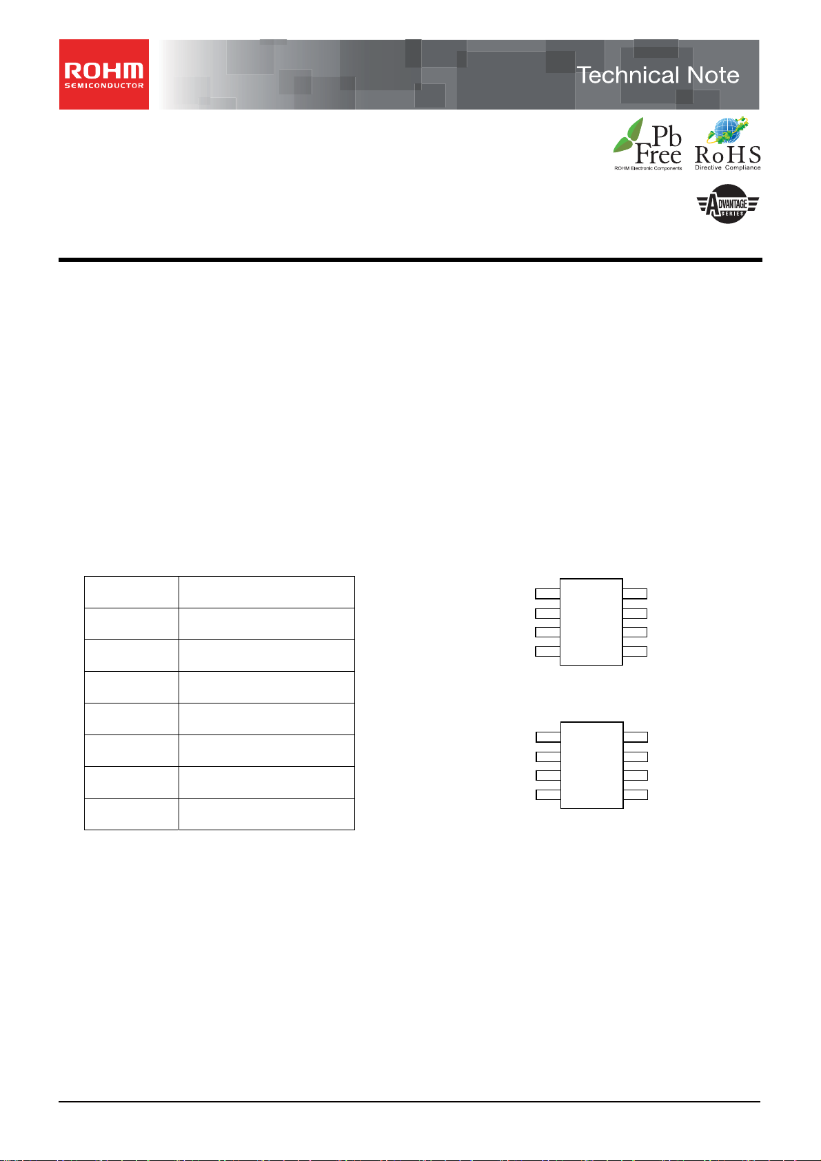
8-lead SOIC Rotated (1K JEDEC only)
DC
VCC
CS
SK
8-lead SOIC
1
2
3
4
1
2
3
4
Figure1.Package
8
7
6
5
8
7
6
5
No.10001EAT12
VCC
DC
DC
GND
DC
GND
DO
DI
www.rohm.com
© 2010 ROHM Co., Ltd. All rights reserved.
1/9
2010.07 - Rev.

A
t
t
BR93C□□-10□U-2.7 family
●Absolute maximum ratings
Table 2: Absolute Maximum Ratings
Parameter Symbol
Ratings
Min. Max.
Unit
Technical Note
Storage Temperature T
Output Range(Q=V
or Hi-Z) V
OH
-65 125 ℃
STG
-0.3 Vcc+0.3 V
out
Input range VIN -0.3 VCC+0.3 V
Supply Voltage VCC -0.3 6.5 V
●Recommended Operating Conditions
Table 3: Recommended Operating Conditions
Parameter Symbol
Supply Voltage VCC
Ambient Operating Temperature TA
Ratings
Min. Max.
2.7 5.5 V
-40 85 ℃
●Block Diagram
Power Source Voltage Detection
CS
Command Decode
Control
Clock Generation
Unit
SK
DI
Command
Register
Address
Buffer
Write
Prohibit
6bi
7bit
8bit
9bit
10bit
Address
Decoder
High Voltage
6bi
7bit
8bit
9bit
10bit
1024 bit
2048 bit
4096 bit
8192 bit
16384 bit
DO
Dummy Bit
Data
Register
16bit
R/W
Amplifier
16bit
EEPROM
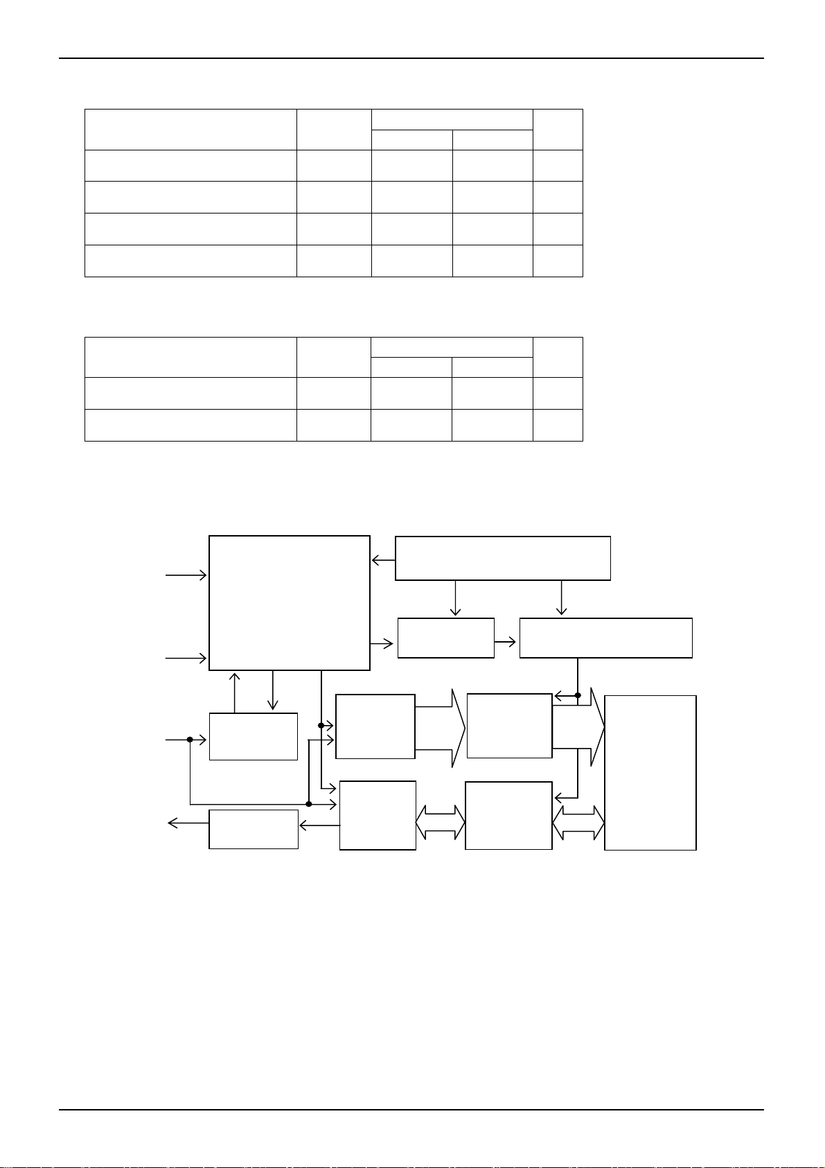
Figure 2: Block Diagram
www.rohm.com
© 2010 ROHM Co., Ltd. All rights reserved.
2/9
2010.07 - Rev.

A
BR93C□□-10□U-2.7 family
●Electrical characteristics
Table 4: DC Characteristics (Unless otherwise specified, Ta=-40-85℃, VCC=2.7-5.5V)
Parameter Symbol
Min. Typ. Max.
Limits
Unit Test Condition
Supply Voltage VCC 2.7 - 5.5 V
Technical Note
Supply Current ICC
Standby Current ISB
- - 2.0 mA VCC=5V, READ at f=1MHz
- - 2.0 mA VCC=5V, WRITE at f=1MHz
- - 10 µA Vcc=2.7V,CS=0V
- - 30 µA Vcc=5.0V,CS=0V
Input Leakage IIL - - 1.0 µA 0V≦VIH≦Vcc
Output Leakage IOL - - 1.0 µA 0≦V
Input Low Voltage
Input High Voltage
Input Low Voltage
Input High Voltage
Output Low Voltage
Output High Voltage
V
IL1
V
IH1
V
IL2
V
IH2
V
OL1
V
OH1
-0.3
2.0
-0.3
0.7VCC
- - 0.4 V
2.4 - - V
0.8V
+0.3
0.2V
V
CC
CC
CC
+0.3
V 4.0V≦VCC≦5.5V
V VCC≦4.0V
2.7V≦V
I
OL
Table 5: AC Characteristics (Unless otherwise specified, Ta=-40-85℃, V
0
0
250
250
250
250
250
250
50
50
100
100
Specification
-
-
-
-
-
-
-
-
-
-
-
-
Parameter
SK Clock Frequency
SK High Time
SK Low Time
Minimum CS Low Time
CS Set-up Time(relative to SK)
DI Set-up Time(relative to SK)
Symbol
fSK
*1
t
SKH
*1
t
SKL
tCS
t
CSS
t
DIS
Min. Typ. Max
=2.7-5.5V)
CC
2
1
-
-
-
-
-
-
-
-
-
-
Unit
MHz
ns
ns
ns
ns
ns
4.5V≦Vcc≦5.5V
2.7V≦Vcc≦5.5V
4.5V≦Vcc≦5.5V
2.7V≦Vcc≦5.5V
4.5V≦Vcc≦5.5V
2.7V≦Vcc≦5.5V
4.5V≦Vcc≦5.5V
2.7V≦Vcc≦5.5V
4.5V≦Vcc≦5.5V
2.7V≦Vcc≦5.5V
4.5V≦Vcc≦5.5V
2.7V≦Vcc≦5.5V
OUT≦VCC
,DO in Hi-Z
≦5.5V
CC
=2.1mA, IOH=-0.4mA
Te st Condition
CS Hold Time(relative to SK)
DI Hold Time(relative to SK)
Output Delay to “1”
Output Delay to “0”
CS to Status Vaid
CS to Do in High Impedance
Write Cycle time
Endurance(5.0V,25℃)
*1: t
+ t
≧1/fc
SKH
SKL
www.rohm.com
© 2010 ROHM Co., Ltd. All rights reserved.
t
0 - - ns
CSH
DIH
t
PD1
t
PD0
- -
t
SV
- -
t
DF
100
- -
- -
100
t
-
-
-
-
250
250
250
250
250
250
100
100
4.5V≦Vcc≦5.5V
ns
2.7V≦Vcc≦5.5V
4.5V≦Vcc≦5.5V
ns
2.7V≦Vcc≦5.5V
4.5V≦Vcc≦5.5V
ns
2.7V≦Vcc≦5.5V
4.5V≦Vcc≦5.5V
ns
2.7V≦Vcc≦5.5V
4.5V≦Vcc≦5.5V
ns
2.7V≦Vcc≦5.5V
tWP - - 10 ms
- 1M - -
Write
Cycle
3/9
2010.07 - Rev.
 Loading...