

Page 1

Artisan Technology Group is your source for quality
new and certied-used/pre-owned equipment
• FAST SHIPPING AND
DELIVERY
• TENS OF THOUSANDS OF
IN-STOCK ITEMS
• EQUIPMENT DEMOS
• HUNDREDS OF
MANUFACTURERS
SUPPORTED
• LEASING/MONTHLY
RENTALS
• ITAR CERTIFIED
SECURE ASSET SOLUTIONS
SERVICE CENTER REPAIRS
Experienced engineers and technicians on staff
at our full-service, in-house repair center
Instra
Remotely inspect equipment before purchasing with
our interactive website at www.instraview.com
Contact us: (888) 88-SOURCE | sales@artisantg.com | www.artisantg.com
SM
REMOTE INSPECTION
View
WE BUY USED EQUIPMENT
Sell your excess, underutilized, and idle used equipment
We also offer credit for buy-backs and trade-ins
www.artisantg.com/WeBuyEquipment
LOOKING FOR MORE INFORMATION?
Visit us on the web at www.artisantg.com for more
information on price quotations, drivers, technical
specications, manuals, and documentation
Page 2

Distributed Power System
SA500 AC Power Modules
615055-1R (14 Amp)
615055-1S (28 Amp)
615055-1T (35 Amp)
615055-1V (48 Amp)
Instruction Manual
Artisan Technology Group - Quality Instrumentation ... Guaranteed | (888) 88-SOURCE | www.artisantg.com
S-3018-1
Page 3

Throughout this manual, the following notes are used to alert you to safety considerations:
ATTENTION:Identifies information about practices or circumstances that can lead to personal
injury or death, property damage, or economic loss.
!
Important: Identifies information that is critical for successful application and understanding of the product.
The thick black bar shown on the left margin of this paragraph will be used throughout this manual to signify
new or revised text or figures.
ATTENTION:Only qualified personnel familiar with the construction and operation of this
equipment and the hazards involved should install, adjust, operate, or service this equipment.
!
Read and understand this manual and other applicable manuals in their entirety before
proceeding. Failure to observe this precaution could result in severe bodily injury or loss of life.
ATTENTION:Only qualified Rockwell personnel or other trained personnel who understand the
potential hazards involved may make modifications to the rack configuration, variable
configuration, and application tasks. Any modifications may result in uncontrolled machine
operation. Failure to observe this precaution could result in damage to equipment and bodily injury .
A TTENTIO N:The user must provide an external, hardwired emergency stop circuit outside of the
drive circuitry. This circuit must disable the system in case of improper operation. Uncontrolled
machine operation may result if this procedure is not f ollowed. Failure to observe this precaution
could result in bodily injury.
ATTENTION:Registers and bits in the UDC module that are described as “read only” or for “system
use only” must not be written to by the user. Writing to these registers and bits may result in
improper system operation. Failure to observe this precaution could result in bodily injury.
ATTENTION:For brushless motor applications, changing any resolver wiring, breaking the
resolver coupling, replacing the resolver, or replacing the motor and resolver for any reason
requires that the shaft alignment test be performed again. Resolv er wiring changes always affect
shaft alignment. A resolver change and/or a new motor/resolver combination will affect the shaft
alignment. Improper shaft alignment can cause motor ov erspeed when the motor is started. Failure
to observe this precaution could result in bodily injury.
ATTENTION:The Power Module contains static-sensitive parts and assemblies. When not
installed in the P ower Module, components should be stored in anti-static bags. F ailure to observe
this precaution could result in damage to, or destruction of, the equipment.
ATTENTION:The user is responsible for conforming with all applicable local, national, and
international codes. Failure to observe this precaution could result in damage to, or destruction
of, the equipment.
The information in this user’s manual is subject to change without notice.
AutoMax™ is a trademark of Rockwell Automation.
©1998 Rockwell International Corporation
Artisan Technology Group - Quality Instrumentation ... Guaranteed | (888) 88-SOURCE | www.artisantg.com
Page 4

Chapter 1 Introduction
1.1 Distributed Power System (DPS) Overview ....................................................1-2
1.2 SA500 Drive Overview .................................................................................... 1-3
1.3 Related Publications........................................................................................1-4
Chapter 2 Power Module Mechanical Description
2.1 LED Indicators.................................................................................................2-3
2.2 Power Module Faceplate Connectors .............................................................2-6
2.2.1 Fiber-Optic Ports ...................................................................................2-7
2.2.2 Rail Ports...............................................................................................2-7
2.2.3 Resolver Feedback Connect or........................................ ....... ...... ....... .. 2-8
2.2.4 Drive I/O Connector ............................................................................2-10
Chapter 3 Power Module Electrical Description
3.1 Power-Up Routine ........................................................................................... 3-1
3.2 DC-to-DC Converter........................................................................................3-2
3.3 Resolver Interface ........................................... ....... ...... ....... ...... ....... ...... ....... .. 3-2
Chapter 4 Installation Guidelines
4.1 Wiring and Grounding...................................................................................... 4-1
4.2 Power Module Installation ...............................................................................4-1
4.3 Fiber-Optic Connection....................................................................................4-6
4.4 Drive I/O Connections ..................................................................................... 4-6
4.5 Rail Port Connection........................................................................................4-8
4.6 Resolver Feedback Connect ion ............................. ...... ....... ...... ....... ...... .........4-8
4.6.1 Resolver Input Connections ............................................ ....... ...... ....... 4-10
4.6.1.1 Resolver Calibration....................................................... ....... 4-11
4.6.1.2 Resolver Alignment........................ ...... .................................4 -12
4.6.1.3 Resolver Feedback Precauti on s ........................................... 4-13
4.6.2 Analog Input........................................................................................4-14
4.7 Constant Power Calibration........................................................................... 4-14
4.8 Power Module Replacement .........................................................................4-17
C
ONTENTS
Chapter 5 Diagnostics and Troubleshooting
Appendix A Technical Specifications...........................................................................................A-1
Appendix B Brushless Industrial Motor Data and Curves............................................................B-1
Appendix C Custom DC Bus Supplies .........................................................................................C-1
Appendix D UDC Register Cross-Reference ...............................................................................D-1
Table of Contents
Artisan Technology Group - Quality Instrumentation ... Guaranteed | (888) 88-SOURCE | www.artisantg.com
5.1 Drive Faults (UDC Register 202/1202)............................................................ 5-1
5.2 Power Module Warnings (UDC Register 203/1203)........................................ 5-3
5.3 Power Module Failure......................................................................................5-4
I
Page 5

Appendix E Status of Data in the AutoMax Rack After a
STOP_ALL Command or STOP_ALL Fault.............................................................E-1
Appendix F PMI Regulator Block Diagram.................................................................................. F-1
Appendix G Power Circuitry Block Diagram ................................................................................G-1
Appendix H Compliance with Electromagnetic Compatibility Standards.....................................H-1
Appendix I SA500 Power Module Output Current Overload Ratings...........................................I-1
Index ...........................................................................................................................Index-1
II
Artisan Technology Group - Quality Instrumentation ... Guaranteed | (888) 88-SOURCE | www.artisantg.com
SA500 Power Modules
Page 6

List of Figures
Figure 1.1 – SA500 Drive Hardware Configuration ..................................................1-2
Figure 2.1 – SA500 Power Module With Cover and Without Cover ......................... 2-2
Figure 2.2 – Power Module External Connectors.....................................................2-6
Figure 2.3 – Location of Rail Fuse on PMI Regulator PC Board .............................. 2-8
Figure 2.4 – Resolver Feedback Connector Pinout.................................................. 2-9
Figure 2.5 – Analog Input Circuit............................................................................ 2-10
Figure 2.6 – Drive I/O Connector Pinout.................................................................2-11
Figure 2.7 – Auxiliary Input Circuit.......................................................................... 2-11
Figure 2.8 – Run Permissive Input (RPI) Circuit..................................................... 2-12
Figure 3.1 – Resolver Data Format (12-Bit Mode)....................................................3-2
Figure 3.2 – Resolver Data Format (14-Bit Mode)....................................................3-3
Figure 3.3 – External Strobe Input Circuit.................................................................3-3
Figure 3.4 – External Strobe Input Circuit Timing Diagram ...................................... 3-4
Figure 4.1 – Power Module Mounting Dimensions...................................................4-3
Figure 4.2 – DC Bus Supply Wiring..........................................................................4-5
Figure 4.3 – Terminal Block Connections for Drive I/O ............................................4-7
Figure 4.4 – Terminal Block Connections for Resolver and Analog Input................ 4-9
Figure 4.5 – Typical Motor Operation in the Constant Torque and
Constant Power Regions....................................................................4-15
Table of Contents
Artisan Technology Group - Quality Instrumentation ... Guaranteed | (888) 88-SOURCE | www.artisantg.com
III
Page 7

IV
SA500 Power Modules
Artisan Technology Group - Quality Instrumentation ... Guaranteed | (888) 88-SOURCE | www.artisantg.com
Page 8

List of Tables
Table 1.1 – SA500 Power Modules.......................................................................... 1-1
Table 1.2 – SA500 Documentation (Binder S-3002) ................................................1-4
Table 4.1 – Recommended Motor Wire Sizes..........................................................4-4
Table 4.2 – Rail I/O Instruction Manuals...................................................................4-8
Table 4.3 – Standard Resolver Connections..........................................................4-10
Table 4.4 – Recommended Resolver Cables.........................................................4-10
Table 4.5 – STATOR_IZ Tunable Values...............................................................4-16
Table of Contents
Artisan Technology Group - Quality Instrumentation ... Guaranteed | (888) 88-SOURCE | www.artisantg.com
V
Page 9

VI
SA500 Power Modules
Artisan Technology Group - Quality Instrumentation ... Guaranteed | (888) 88-SOURCE | www.artisantg.com
Page 10

C
HAPTER
1
Introduction
The AutoMax Distributed Power System SA500 AC Power Modules provide AC power
to, and control of, brushless motors and squirrel-cage induction motors from 1–15HP.
Each Power Module contains the Power Module Interface (PMI) Regulator printed
circuit board and the inverter used to convert DC power to AC power for the motor.
Depending upon their power requirements, up to six Power Modules can be
daisy-chained together and operated from one SA500 DC Bus Supply, which provides
the Power Modules a nominal 325 VDC input power. The DC Bus Supply is described
in instruction manual S-3017.
The SA500 Power Modules are available in four sizes with a range of current ratings to
complement the variety of motors available. See table 1.1 below.
Table 1.1 – SA500 Power Modules
Maximum Output
Current (RM S)
(0.5 seconds)
1
Part Number
Continuous Current
Rating (RMS)
615055-1R 14 A 17.5 A (125%)
615055-1S 28 A 35 A (125%)
615055-1T 35 A 70 A (200%)
615055-1V 48 A 106 A (220%)
1. Power Module output current overload rating charts are provided in Appendix I.
Power Module specifications are listed in Appendix A. Detailed speed-torque curves
and engineering data f or SA500 motors are included in Appendix B.
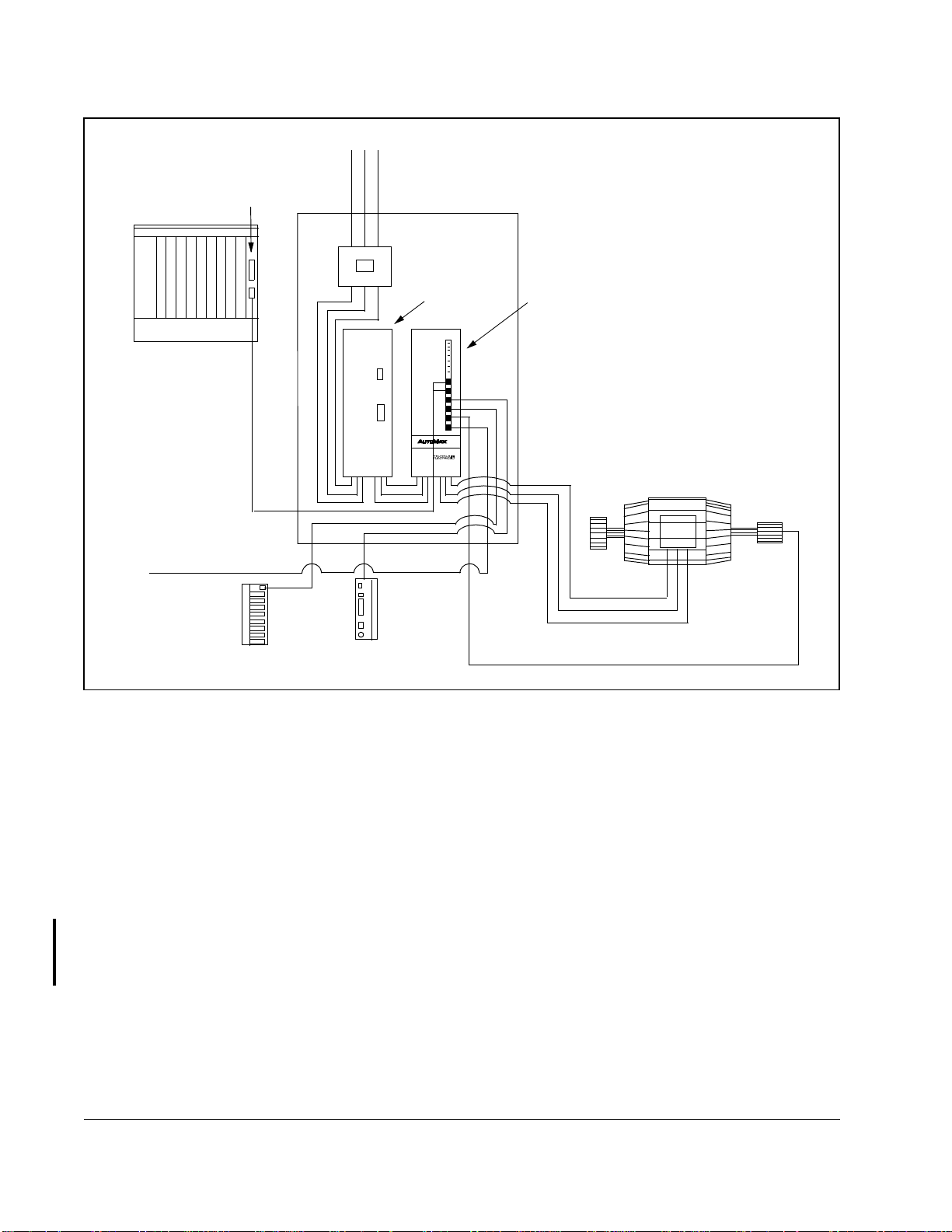
Figure 1.1 shows a typical SA500 drive configuration.
Introduction
1-1
Artisan Technology Group - Quality Instrumentation ... Guaranteed | (888) 88-SOURCE | www.artisantg.com
Page 11
Universal Drive
Controller Module
AutoMax Rack
Fiber-Optic Link
(up to 750 m)
Drive I/O
AC Line
SA500
DC Bus
Supply
SA500
Power
Module
Resolver
Motor
Digital Rail Analog Rail
Figure 1.1 – SA500 Drive Hardware Configuration
Resolver Fe edback
1.1 Distributed Power System (DPS) Overview
The SA500 is a member of the AutoMax Distributed Power System (DPS) family of
drives. DPS is a programmable microprocessor-based control system that is capable
of real-time control of AC and DC drives. Each Universal Drive Controller (UDC)
module (B/M O-57552) in the AutoMax rack allows the AutoMax Processor to control
up to two drives (20 maximum from one rack). The UDC module communicates over a
fiber-optic link with the PMI located in the SA500 Power Module. The Power Module
can be located up to 750 meters (2500 feet) from the AutoMax rack.
Each DPS drive is controlled by an application task running in the UDC module. All
programming and configuration of the SA500 drive is performed using the AutoMax
Programming Executive software. The SA500 drive requires version 3.4 or later of the
Programming Executive.
1-2
SA500 Power Modules
Artisan Technology Group - Quality Instrumentation ... Guaranteed | (888) 88-SOURCE | www.artisantg.com
Page 12

1.2 SA500 Drive Overview
An SA500 drive consists of a DC Bus Supply and a Power Module which supplies
three-phase AC power to an induction motor or a permanent magnet brushless motor .
The SA500 DC Bus Supply rectifies three-phase 230 VA C power to provide a constant
DC voltage for the Pow er Module. A three-phase bridge consisting of three SCRs and
three diodes controls the currents during charging of the DC bus capacitor. During
charging, the phase angle of the SCR firing is shifted as a function of time to control
the charging current.
The DC Bus Supply includes a braking circuit, consisting of a bi-polar transistor switch
and a resistor. A DC-to-DC converter within the Power Module senses the DC bus
voltage and switches the braking resistor across the DC bus if a preset threshold is
exceeded. If the capacity of the internal braking resistor is exceeded, the drive’s ability
to dissipate energy may be increased by using an external braking resistor. See
instruction manual S-3017 for more information.
Depending upon the power drawn by the individual Power Modules, the DC Bus
Supply can support up to six Power Modules, each powering one motor. If more than
six Power Modules need to be supplied by a common DC bus, if the capacity of the
DC bus is exceeded, or if the capacity of the braking circuit is exceeded, a
custom-designed DC b us supply may be used with the SA500 Power Modules. The
custom DC bus may be regenerative or non-regenerative. Energy storage capacitors
must be provided with the custom DC bus (or separately). See Appendix C for more
information.
The SA500 Power Module consists of the PMI Regulator (commonly referred to as the
PMI) and power circuitry to invert the DC bus voltage to three-phase 230 VAC for the
motor. The power bridge consists of six bipolar transistors (three dual-transistor
modules).
The PMI receives its operating system, all configuration data, and all commands
including the torque reference from a UDC module in the AutoMax rack via fiber-optic
cables. The PMI executes the torque control algorithm that controls the motor. The
control type is determined by the operating system contained in the PMI. There are
four types of control available: 1) vector, 2) brushless, 3) vector - speed loop
enhanced, and 4) brushless - speed loop enhanced. The operating system is selected
during UDC module configuration.
The UDC module executes the outer (major) control loops. The UDC task (task A or
task B, depending upon the fiber-optic port to which the Power Module is connected)
controls drive sequencing and the alignment of the resolver in brushless applications.
The UDC task provides the torque ref erence to the PMI and communicates with other
upper-level control tasks in the AutoMax rack.
The UDC module and the PMI are tightly synchronized through the fiber-optic link.
The PMI sends all feedback signals, including warning and fault information, speed
feedback, rail data, and gain data, to the UDC before each UDC task scan. Speed
feedback sampling in the Power Module is synchronized to within 1 µsec of the UDC
scan. The operating system in the PMI continuously performs diagnostic checks and
displays the results on the Power Module faceplate LEDs.
Introduction
The PMI also provides connections to digital and analog rails, as well as digital drive
I/O. The PMI scans the rail and drive I/O while the regulation algorithm is running. This
permits the I/O data to be integrated into the control algorithm as required.
1-3
Artisan Technology Group - Quality Instrumentation ... Guaranteed | (888) 88-SOURCE | www.artisantg.com
Page 13
1.3 Related Publications
This instruction manual provides a description of the SA500 Power Module hardware.
Installation guidelines are also provided. Note that this instruction manual does not
describe specific applications of the standard hardware or software.
For more information, refer to the instruction manuals contained in the SA500 drive
binder, S-3002, as listed in table 1.2. It is assumed that the user is familiar with these
other manuals in S-3002 before installing, operating, or performing maintenance upon
SA500 Power Modules. Refer to these instruction manuals as needed.
:
7DEOH ¤ 6$ 'RFXPHQWDWLRQ %LQGHU 6
Document Document Part Number
DPS Overview S-3005
Universal Drive Controller Module S-3007
Fiber Optic Cabling S-3009
SA500 DC Bus Supply S-3017
SA500 AC Power Modules S-3018
SA500 Diagnostics, Troubleshooting, & Start-Up
S-3022
Guidelines
SA500 Information Guide S-3024
SA500 Drive Configuration & Programming S-3044
Additional information about using SA500 Power Modules is found in the other
instruction manuals, prints, and documents shipped with each drive system. Always
consult the prints shipped with the drive system for specific mounting and connecting
information about your drive.
1-4
SA500 Power Modules
Artisan Technology Group - Quality Instrumentation ... Guaranteed | (888) 88-SOURCE | www.artisantg.com
Page 14

C
HAPTER
2
Power Module Mechanical Description
Power Modules of all four ratings are the same size, consisting of a sheet metal
enclosure, cooling fans, heatsink, a power supply PC board, inverter power devices,
and the PMI Regulator PC board. A DC-to-DC converter supplies power to the PMI
and to Hall-effect devices used for current feedback.
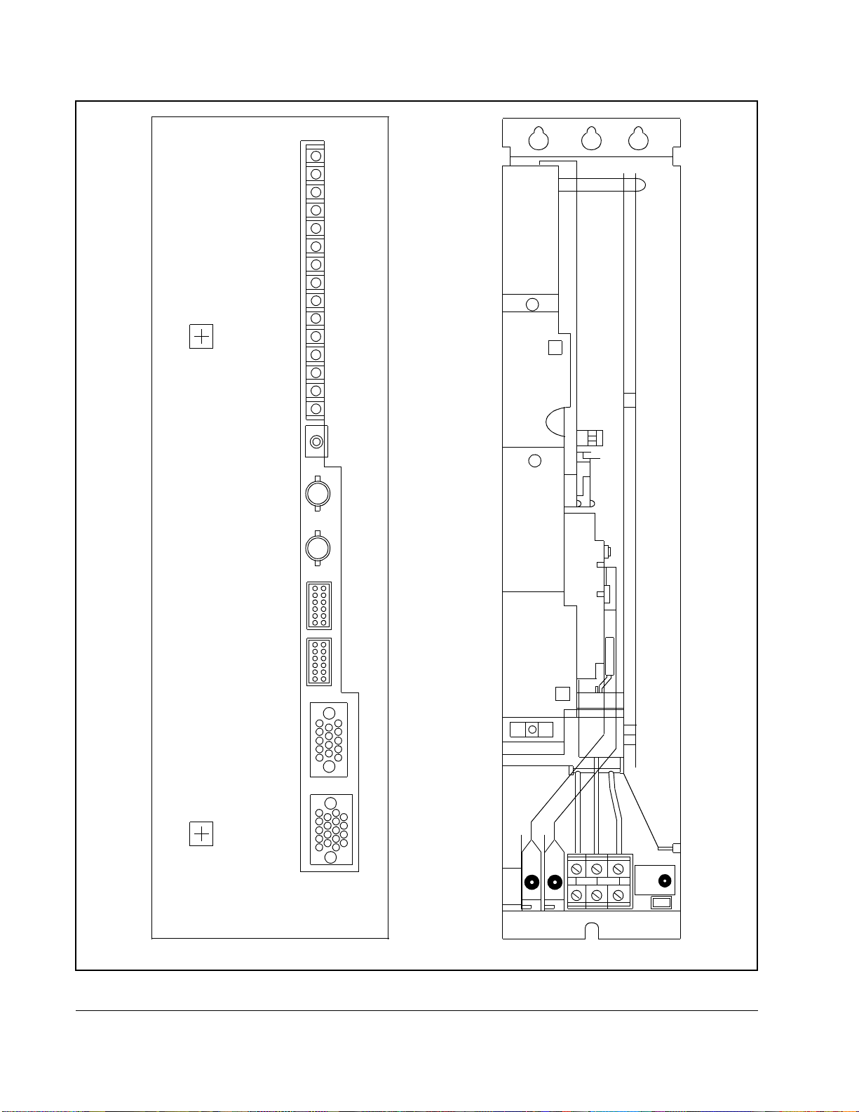
The faceplate of the Power Module has 15 LEDs, two rail I/O ports, fiber-optic transmit
and receive ports, a resolver f eedback connector for speed feedback and analog input
signals, and a drive I/O connector for dedicated and general-purpose drive I/O. A
push-button labeled “RE-BOOT” allows the PMI Regulator to be reinitialized. This
allows ne Power Module to be reset without powering down the entire DC bus and all
the Power Modules on it. When the button is pressed, all I/O is reset, the PMI executes
its power-up routine, and then requests its operating system from the UDC module.
The SA500 Power Module is cooled by forced air . Air enters through the bottom of the
module and exits through the top . The two f ans at the bottom of the Power Module are
internally connected and powered via a 24V supply produced by the DC-to-DC
converter. The PMI monitors the temperature of the Power Module heatsink and
reports an overtemperature condition in register 202/1202, bit 0.
Two quarter-turn fasteners on the faceplate allow removal of the Power Module cover.
Mounting holes are provided on flanges that extend above and below the module.
Module dimensions are listed in Appendix A. See figure 2.1 for views of the module
with and without its cover.
Note that motor-mounted resolvers are required for speed and position feedback on
SA500 drives. Resolvers are included with every SA500 brushless and induction
motor.
Power Module Mechanical Description
Artisan Technology Group - Quality Instrumentation ... Guaranteed | (888) 88-SOURCE | www.artisantg.com
2-1
Page 15
PWR OK
OK
COMM OK
P.M. FLT
EXT FLT
RAIL FLT
FDBK OK
RPI
MCR
AUX IN1
AUX IN2
AUX IN3
AUX IN4
AUX IN5
AUX OUT
RE-BOOT
XMT
COMM
LINK
RCV
P1
P2
P3
RAIL
PORT 0
P4
RAIL
PORT 1
P5
RESOLVER
FEEDBACK
P6
DRIVE I/O
WITH COVER ON WITH COVER REMOVED
Figure 2.1 – SA500 Power Module With Cover and Without Cover
2-2
SA500 Power Modules
Artisan Technology Group - Quality Instrumentation ... Guaranteed | (888) 88-SOURCE | www.artisantg.com
Page 16

2.1 LED Indicators
The LEDs on the faceplate of the Power Module indicate the status of the PMI,
inverter, fiber-optic link, rail I/O, resolver feedback signal, and drive I/O. The status of
the LEDs is also reported in the UDC module’s dual port memory. See the SA500
Drive Configuration and Programming instruction manual (S-3044) for a complete
description of the following status bits. Note that all faults indicated by the LEDs
(except for the RAIL FLT LED) will result in the PMI disabling the power device gates,
which will cause the motor to coast to a stop.
The LED indicators on the module faceplate are defined as follows:
PWR OK
OK
COMM OK
(green) - The “PWR OK” LED indicates that all power supply voltages
for the PMI are at acceptable operating levels. The status of
the DC-to-DC converter is available in the UDC module’s dual
port memory (register 202/1202, bit 12). This LED also
indicates that the DC bus is powered up.
(green) - When power is applied to the P ower Module, the LED will turn
on to indicate the PMI has passed its internal power-up
diagnostics. After power-up, this LED will turn off if the
internal watchdog times out. This will cause the drive to
disable the gate drive circuitry in the inverter.
(green) - When lit, this LED indicates messages are being received
correctly over the fiber-optic link from the UDC module. If this
LED is off, it indicates there is a fault in the link or that the
UDC module is unable to communicate.
If the PMI does not receiv e a message from the UDC module
for two or more CCLK periods, or logs two consecutive
communication errors of any type, the PMI processor will shut
the drive down.
Detailed information about the communication link (e.g.,
number of messages sent and received, CRC error count) is
displayed in the UDC/PMI Communication Status Registers
(80-89/1080-1089) on the UDC module.
P.M. FLT
Power Module Mechanical Description
Artisan Technology Group - Quality Instrumentation ... Guaranteed | (888) 88-SOURCE | www.artisantg.com
(red) - When lit, this LED indicates that one of the fault conditions
listed below has been detected in the Power Module:
•
Overtemperature
Corresponding UDC location: Register 202/1202, bit 0
•
DC bus overvoltage
Corresponding UDC location: Register 202/1202, bit 2
•
Vcc (+5V) supply undervoltage
Corresponding UDC location: Register 202/1202, bit 3
2-3
Page 17

EXT FLT (red) - When lit, this LED indicates that one of the following external
fault conditions has occurred:
•
Overcurrent fault
Corresponding UDC location: Register 202/1202, bit 1
•
User-programmed fault
Corresponding UDC location: Register 101/1101, bit 2
•
Overspeed fault
Corresponding UDC location: Register 202/1202, bit 10
RAIL FLT (red) - When lit, this LED indicates communication between an I/O
rail and the PMI has been disrupted, or that a rail has been
configured but is not plugged in.
Registers 0-23 are available in the UDC module for rail
variable configuration and diagnostic purposes. If a rail
communication problem is detected and logged in register 4,
10, 16, or 22, then bit 13 in the Drive Warnings register
(203/1203) will be set.
Note that rail faults will not cause the drive to shut down. The
user must ensure that the application task tests the rail fault
registers and forces appropriate action in the event of a fault.
FDBK OK (green) - When lit, this LED indicates that the Resolver & Drive I/O
module is receiving feedback from the resolver and that no
resolver feedback faults have been detected.
If the LED is off, it indicates the following fault:
•
Feedback broken wire fault. The resolver sine and/or
cosine signals are missing, or the resolver gain tunable
(RES_GAN%) has been set too low.
Corresponding bit location: Register 202/1202, bit 8
The signals associated with the following LEDs interface to the Power Module via the
Drive I/O connector. See figure 2.6.
RPI (green) - When lit, this LED indicates that the run permissive input
(RPI) signal is detected on pin A. The RPI signal typically
originates from the drive's coast-to-rest stop circuit.
Corresponding bit location: Register 201/1201, bit 0.
MCR (amber) - When lit, this LED indicates the MCR (motor control relay)
output signal is being driven on (pin P). The MCR output is
under the control of the PMI. This LED will turn on when the
drive is put into run and will turn off when the drive is idle. The
use of a motor control relay is optional.
2-4
SA500 Power Modules
Artisan Technology Group - Quality Instrumentation ... Guaranteed | (888) 88-SOURCE | www.artisantg.com
Page 18

AUX IN1 (green) - When lit, this LED indicates the presence of a 115 volt signal
on this input (pin C). This LED is used for M-contactor
feedback when the programmer has configured an output
contactor between the Power Module and the motor. The use
of an M-contactor is optional.
Corresponding bit location: Register 201/1201, bit 1.
AUX IN2 (green) - When lit, this LED indicates the presence of a 115 volt signal
on this input (pin E).
Corresponding bit location: Register 201/1201, bit 2.
AUX IN3 (green) - When lit, this LED indicates the presence of a 115 volt signal
on this input (pin H).
Corresponding bit location: Register 201/1201, bit 3.
AUX IN4 (green) - When lit, this LED indicates the presence of a 115 volt signal
on this input (pin K).
Corresponding bit location: Register 201/1201, bit 4.
.
AUX IN5 (green) - When lit, this LED indicates the presence of a 115 volt signal
on this input (pin M).
Corresponding bit location: Register 201/1201, bit 5.
.
AUX OU T (amber) - When lit, this LED indicates the output signal has been
turned on (pin S).
Corresponding bit location: Register 101/1101, bit 4.
Power Module Mechanical Description
Artisan Technology Group - Quality Instrumentation ... Guaranteed | (888) 88-SOURCE | www.artisantg.com
2-5
Page 19
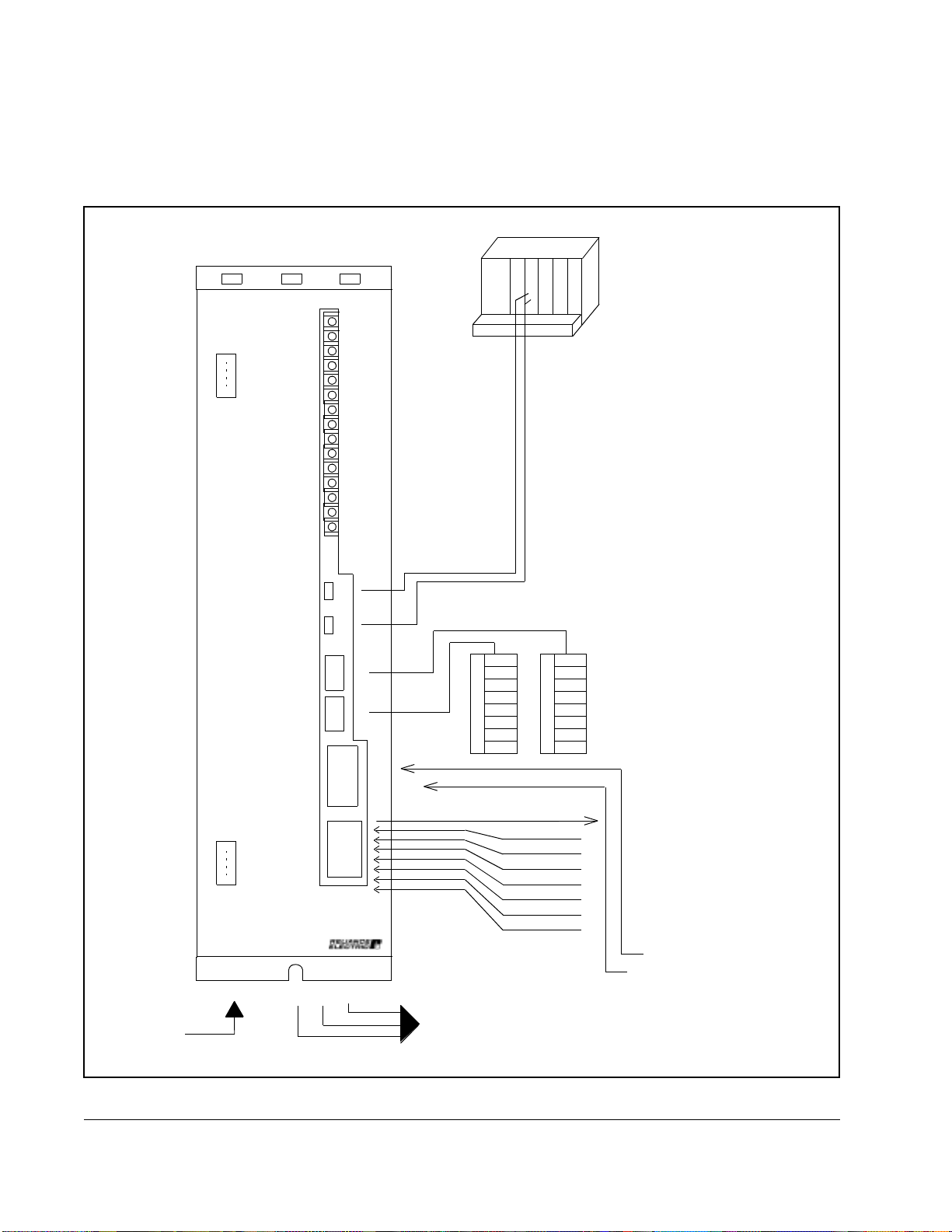
2.2 Power Module Faceplate Co nnectors
The following sections describe the Power Module faceplate connectors. Figure 2.2
shows the external connections to the Power Module.
CU
PS
DCP
U
PWR OK
OK
COMM OK
P.M. FLT
EXT FLT
RAIL FLT
FDBK OK
RPI
MCR
AUX IN1
AUX IN2
AUX IN3
AUX IN4
AUX IN5
AUX OUT
RE-BOOT
AutoMax
FROM
D-C BUS
SUPPLY
XMTCOMM
LINK
RCV
RAIL
PORT 0
RAIL
PORT 1
RESOLVER
FEEDBACK
DRIVE I/O
AutoMax SA500
DISTRIBUTED POWER SYSTEM
AC POWER MODULE
POS NEG U V W GND
RAIL I/O
MCR
AUX IN1
AUX IN2
AUX IN3
AUX IN4
AUX IN5
AUX OUT
RPI
RESOLVER FEEDBACK
ANALOG INPUT
TO MOTOR
2-6
Figure 2.2 – Power Module External Connectors
SA500 Power Modules
Artisan Technology Group - Quality Instrumentation ... Guaranteed | (888) 88-SOURCE | www.artisantg.com
Page 20

2.2.1 Fiber-Optic Ports
Transmit (XTM) and receive (RCV) ports are provided on the faceplate of the Power
Module for connection to the fiber-optic link with the UDC module in the AutoMax rack.
The Power Module is shipped with dust caps covering the fiber-optic ports. To prevent
dust accumulation and the resulting loss of signal integrity, the dust caps should not
be removed until the fiber-optic cables are installed, and should be replaced if the
cables are disconnected.
!
2.2.2 Rail Ports
Two rail ports (0 and 1) on the faceplate of the Power Module support direct
connection to digital and analog rail modules. All combinations of the modules listed
below are supported.
•
M/N 45C001A
•
M/N 45C630
•
M/N 45C631
•
M/N 61C345
•
M/N 61C346
•
M/N 61C350
•
M/N 61C351
•
M/N 61C365
•
M/N 61C366
ATTENTION:
the UDC module and to its corresponding PMI Regulator before viewing
the fiber-optic cable or transmitter under magnification. Viewing a
powered fiber-optic transmitter or connected cable under magnification
may result in damage to the eye. For additional information ref er to ANSI
publication Z136.1-1981. Failure to observe this precaution could result
in bodily injury.
Digital I/O Rail (J-3012)
4-Decade Thumbwheel Switch Input Module (J-3654)
4-Digit LED Output Module (J-3655)
4-Channel Analog Current Input Rail (J-3689)
4-Channel Analog Voltage Input Rail (J-3688)
2-Channel Analog Voltage Input/Output Rail (J-3672)
2-Channel Analog Current Input/Output Rail (J-3673)
4-Channel Analog Current Output Rail (J-3694)
4-Channel Analog Voltage Output Rail (J-3695)
T urn off, lock out, and tag power to both the rack containing
Digital I/O modules can be mixed in an I/O rail connected to the P ower Module. Analog
rail modules must be used in the rail mode only. Note that Local Heads (M/N 61C22)
are not supported.
These rails receive the 5V power required for their operation through their connection
to the PMI. If the PMI is reset or power is removed, all outputs are turned off. Rail
cables must not be connected or disconnected under power.
The PMI contains the fusing f or the rail I/O. The P ower Module cov er must be removed
to replace the rail fuse. See figure 2.3 for the location of the rail fuse. See Appendix A
for the rail fuse specification.
The rail update rate is asynchronous to the UDC task and UDC-to-PMI
communications. While the regulation algorithm is running, digital rails are updated
every 5 msec (both ports). Analog rails are updated every 20 msec (both ports).
Power Module Mechanical Description
Artisan Technology Group - Quality Instrumentation ... Guaranteed | (888) 88-SOURCE | www.artisantg.com
2-7
Page 21
RIGHT SIDE VIEW
RAIL FUSE
FAN
POWER
2-8
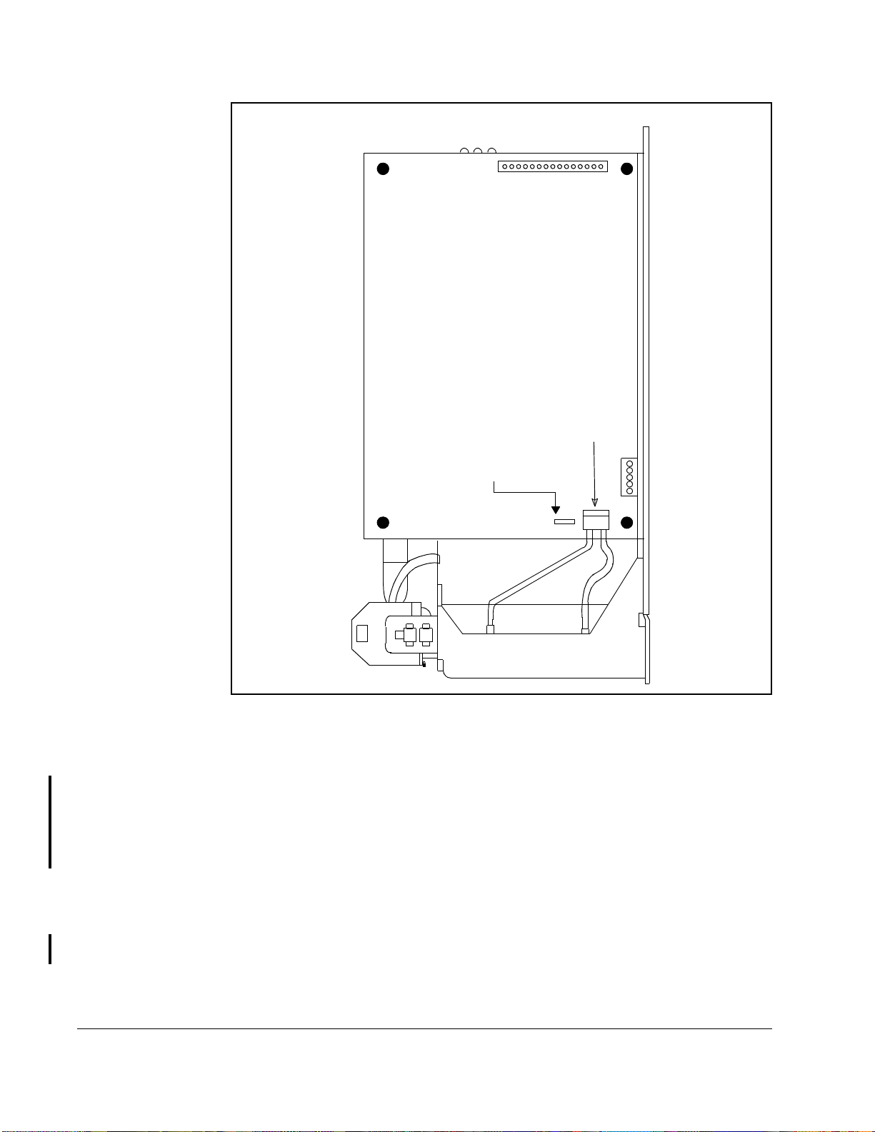
Figure 2.3 – Location of Rail Fuse on PMI Regulator PC Board
2.2.3 Resolver Feedback Connector
The faceplate connector labeled “RESOLVER FEEDBACK” is used to connect the
resolver to the Power Module. This connector will also accept a signal from an analog
tachometer or other analog field device as long as the signal is within the correct
voltage range. (Note that the tachometer cannot be used for speed feedback.) A 24V
digital input that serves as a strobe for latching the resolver position externally is also
supplied.
Both a resolver and an analog device may be connected to the module (e.g., the
analog input may be used for tension or position feedback at the same time that the
resolver input is used for speed feedback). However, only the resolver will be
monitored for an overspeed condition. See the SA500 Drive Configuration and
Programming instruction manual, S-3044, for more information.
SA500 Power Modules
Artisan Technology Group - Quality Instrumentation ... Guaranteed | (888) 88-SOURCE | www.artisantg.com
Page 22
ATTENTION:For brushless motor applications, changing any resolver
wiring, breaking the resolver coupling, replacing the resolver , or replacing
!
the motor and resolver for any reason requires that the shaft alignment
test be performed again. Resolver wiring changes always affect shaft
alignment. A resolver change and/or a new motor/resolver combination
will affect the shaft alignment. Improper shaft alignment can cause motor
overspeed when the motor is started. F ailure to observe this precaution
could result in bodily injury.
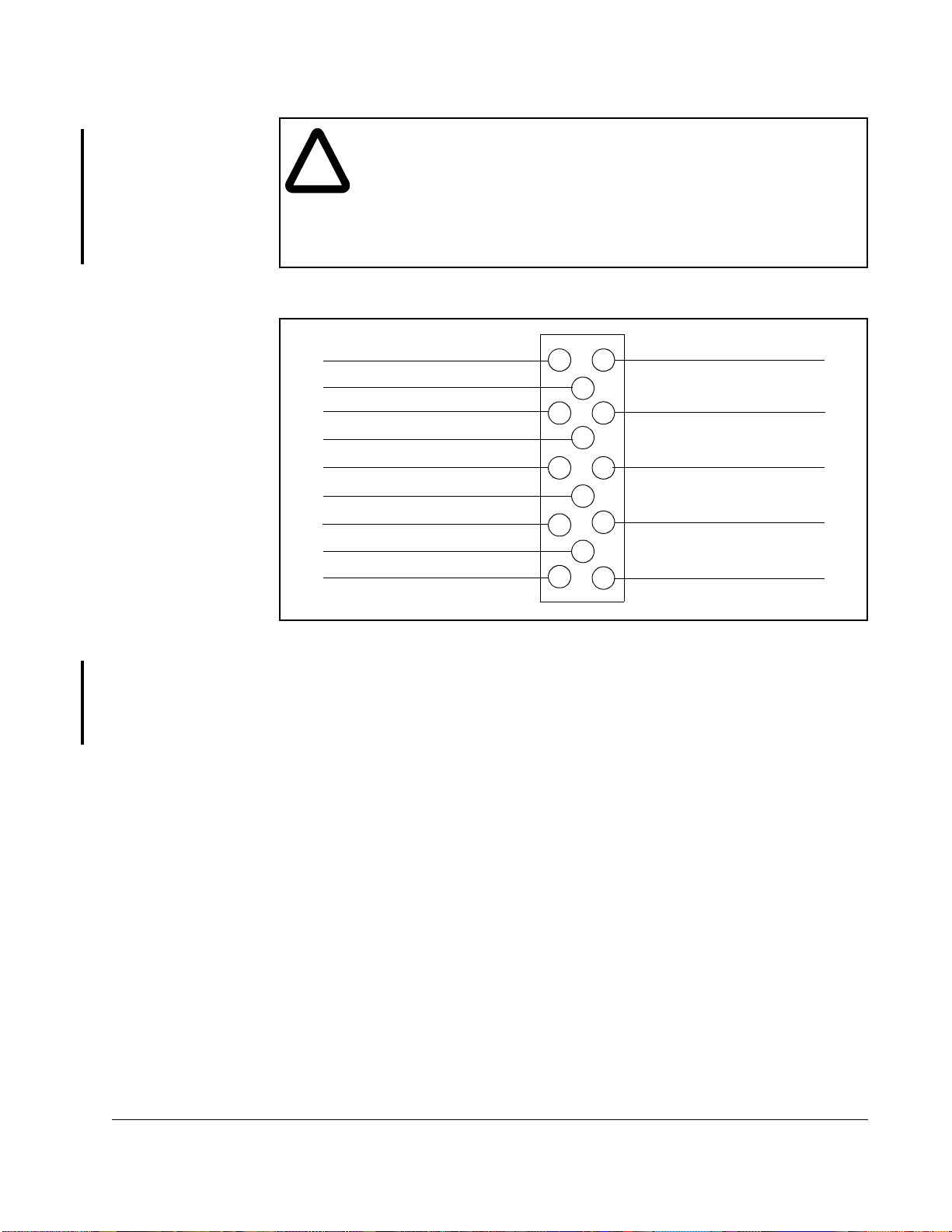
The Resolver Feedback connector pinout is shown in figure 2.4.
Reference Out (+)
Reference Out (-)
Sine Input (+)
Cosine Input (+)
External Strobe Input (+)
External Strobe Input (-)
Not Used
Not Used
Analog Input (+)
Figure 2.4 – Resolver Feedback Connector Pinout
A
B
D
E
H
J
L
M
P
Sine Input (-)
C
Cosine Input (-)
F
K
Key Pin
N
Analog Input (-)
Analog Input Shield
R
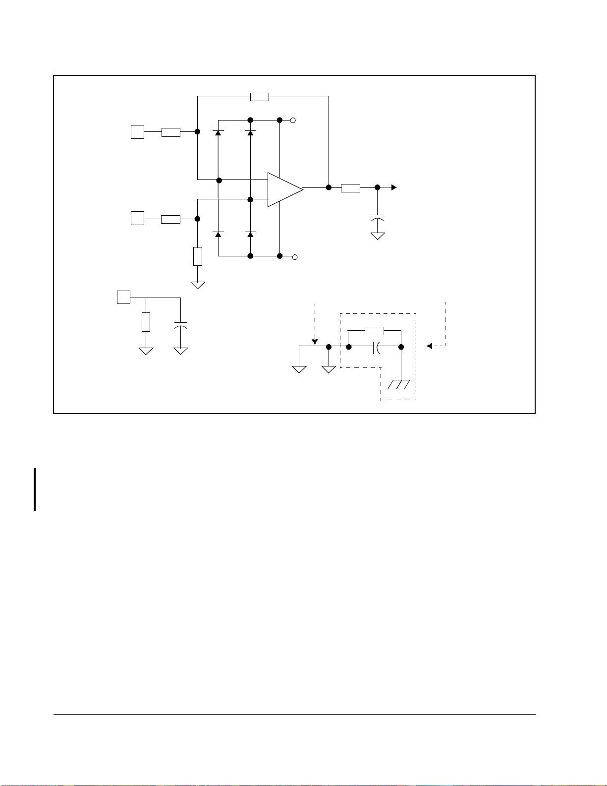
The analog input operates over the range of +/-10V differential (+/-30V common
mode). It is the user's responsibility to ensure that the input signal is scaled to conform
to this range. The input is bandwidth-limited to 320 Hz. The resolution of the input is
12 bits (11 bits plus sign) or 4.88 mV per bit. The input impedance is 1.3 megohms
and is resistively isolated. The analog input circuit is shown in figure 2.5.
If an analog tachometer is not used, the input may be used f or other purposes as long
as the signal is within the correct voltage range. The PMI sends the analog input data
to the UDC module immediately before it is needed by the UDC module for the next
UDC task scan. The analog input data is stored in UDC register 214/1214. The v alue
may range from -2048 (-10 volts) to +2047 (+10 volts).
Power Module Mechanical Description
Artisan Technology Group - Quality Instrumentation ... Guaranteed | (888) 88-SOURCE | www.artisantg.com
2-9
Page 23
312K
ANALOG -
ANALOG+
ANALOG SHIELD
1K
AGND
1.04M
1.04M
312K
DGND
.33
F
µ
AGND
+15 V
–
+
-15 V
THIS CONNECTION
IS MADE WITH THE
DC/DC CONVERTER
DGND
AGND
20K
5600 pF
TO A/D
SUBSYSTEM
AGND
THESE COMPONENTS
ARE ON THE PMI
REGULATOR
10K
.33 µF
Figure 2.5 – Analog Input Circuit
2.2.4 Drive I/O Connector
The connector labeled “DRIVE I/O” is used for digital I/O connections to standard
drive-related signals, such as M-contactor status, the run permissive input (RPI) for
the drive, or for other user-designated functions. Six digital inputs and two digital
outputs are provided. Five of the inputs (AUX IN1 to AUX IN5) and one of the outputs
are user-programmable.
The digital drive I/O operates with 115VAC (50/60Hz) nominal line voltage. All input
and output channels have isolated commons with an isolated voltage rating limited to
150VAC. All inputs and outputs have isolation voltage ratings of 1500 volts between
the I/O and the PMI Regulator's power supply. See figures through for the input and
output circuit diagrams.
The RPI input and the MCR output are interlocked in hardware on the module. The
MCR output is activated only when the RPI signal is asserted (by the user) and the
MCR output is being commanded on by the PMI. The PMI will begin the process to
turn off the MCR output when any of the following conditions occurs:
•
The RPI input signal is removed
•
A drive fault occurs
•
The torque control algorithm is turned off (TRQ_RUN = 0)
2-10
SA500 Power Modules
Artisan Technology Group - Quality Instrumentation ... Guaranteed | (888) 88-SOURCE | www.artisantg.com
Page 24
If any of these events occurs, the PMI will wait f or 100 msec and then turn off the MCR
RPI IN (+)
AUX IN2 (+)
AUX IN1/MFDBK (+)
AUX IN3 (+)
AUX IN4 (+)
AUX IN5 (+)
MCR OUT (+)
AUX OUT (+)
Key Pin
A
C
E
H
K
M
P
S
U
B
D
F
J
L
N
R
T
V
RPI IN (-)
AUX IN1/MFDBK (-)
AUX IN2 (-)
AUX IN3 (-)
AUX IN4 (-)
AUX IN5 (-)
MCR OUT (-)
AUX OUT (-)
Not Used
330
15K
182
DIGITAL
OUT TO
MICROPROCESSOR
.1uF
AUX INPUTS
output. If the RPI signal is remov ed, the MCR output will be turned off and gate pow er
will be removed under hardware control within approximately 0.5 second to provide an
additional level of protection.
The user has the option of having an M-contactor (i.e., an output contactor) on the
output of the Power Module. This option is available during UDC parameter
configuration. The M-contactor is controlled by the MCR output, which is under the
control of the PMI processor. If the choice is made to connect the MCR to the output
contactor, the contacts must be wired to the AUX IN1/MFDBK input. The PMI will then
wait for this signal to turn on before executing the control algorithm. The status of the
AUX IN1/ MFDBK input is reported in register 201/1201, bit 1. If this configuration
choice is not made, the AUX IN1 input can be used for any user-designated purpose.
The status of the drive I/O is indicated in UDC register 201/1201 and by eight LEDs on
the module faceplate. In the event of a power loss or if a system reset command is
initiated by the PMI, all outputs are turned off.
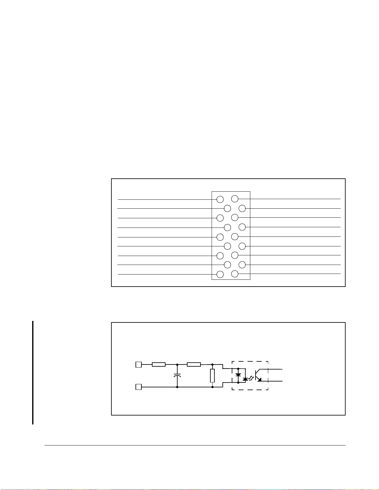
The Drive I/O connector pinout is shown in figure 2.6.
Power Module Mechanical Description
Figure 2.6 – Drive I/O Connector Pinout
Figure 2.7 shows the auxiliary input interface circuit.
Artisan Technology Group - Quality Instrumentation ... Guaranteed | (888) 88-SOURCE | www.artisantg.com
The run permissive input (RPI) circuit is shown in figure 2.8.
Figure 2.7 – Auxiliary Input Circuit
2-11
Page 25
DGND = ON
+15V
GATE KILL
+15V = OFF
DGND
MCR_OUT+
MCR_OUT-
6
124
5
3
1 = On
Other Faults
0 = Off
10
3 4
+5V
–
+
1
8
1/2
Second
Delay
M-Contactor
12
DGND
1
+
-
+
6
7
+15V
7
-
6
1
+5V +5V
+
–
DGND
6
4
1
3
Shunt
Regulator
3
2
2-12
RPI_IN+
RPI_IN-
Figure 2.8 – Run Permissive Input (RPI) Circuit
SA500 Power Modules
Artisan Technology Group - Quality Instrumentation ... Guaranteed | (888) 88-SOURCE | www.artisantg.com
Page 26

C
HAPTER
3
Power Module Electrical Description
DC input voltage to the Power Module is supplied by a DC bus, normally the SA500
DC Bus Supply. The inverter bridge in the Power Module converts the constant
potential DC voltage from the DC bus to three-phase AC power for the motor. The
inverter bridge consists of six bi-polar transistors. Interlock circuitry ensures that the
upper phase and lower phase U, V, and W transistors are never turned on at the same
time.
The inverter bridge can regenerate energy to the DC bus. During regeneration, the
inverter returns energy from the motor to the DC bus. Howev er, the SA500 DC Bus
Supply cannot pass this regenerative current back to the AC line. Instead, it stores the
excess energy in its capacitors. It can then pass this surplus energy to other Power
Modules on the bus that need motoring current, or it can dissipate the energy through
DC bus braking resistors. See the DC Bus Supply instruction manual (S-3017) for
specifications on the regeneration limits of the DC Bus Supply and for more
information about braking resistors.
The regulator circuitry and UDC communication interface is contained on a single PC
board, the Power Module Interface (PMI) Regulator. This PC board contains control
circuitry for the inverter, resolver and drive I/O circuitry, and fiber-optic transceivers for
communication with the UDC module in the AutoMax rack. The PMI’s main function is
torque regulation for brushless motors and induction motors.
The PMI contains a RISC (reduced instruction set computer) microprocessor
operating at 16 MHz. High speed communication with the UDC module is controlled
by an onboard serial communications controller. Data is transmitted over the
fiber-optic link at 10 Mbit/sec using the High-Le vel Data Link Control (HDLC) protocol.
Data integrity is checked using a CRC (cyclic redundancy check) error detection
scheme.
The PMI contains an on-board watchdog timer that is enabled when power is applied
to the PMI. Once activated, the on-board CPU must continually reset the watchdog
timer within a specified time or the PMI will shut down. The MCR output, typically used
to control a motor contactor, will be turned off under hardware control within 0.5
seconds if the watchdog times out. (The MCR output is also turned off if the RPI input
turns off.) To reset the watchdog, you must either cycle power or press the RE-BOOT
button on the faceplate.
Any faults in the Po wer Module will cause the PMI to turn off the control signals to the
power devices (bipolar transistors) that switch the DC bus voltage to the motor.
3.1 Power-Up Routine
When power is applied to the Power Module, the LEDs will blink three times as a test
and the PMI will perform a series of internal diagnostics. The P.M. FLT LED on the
faceplate will flash if the Power Module fails any of these diagnostics. If the diagnostics
are passed, the OK LED on the faceplate will turn on.
Power Module Electrical Description
Artisan Technology Group - Quality Instrumentation ... Guaranteed | (888) 88-SOURCE | www.artisantg.com
3-1
Page 27

The PMI will automatically request its operating system from the UDC module as soon
as communications are established over the fiber-optic link. After the operating system
has been downloaded from the UDC module (a process that takes approximately 0.5
seconds), the PMI Regulator will send a feedback message. The UDC module will
respond with a command message and configuration data. The information sent
contains configuration data as well as the synchronization information necessary for
the PMI to determine when to send feedback messages to the UDC module once
UDC application tasks are put into run.
The PMI uses non-volatile EPROM memory to store the initial start-up software and
power-up diagnostics and to establish communication with the UDC module. After
power-up, the module stores data in and operates out of volatile SRAM. If power is
removed from the Power Module, all data and the module’s operating system will be
lost. When power is returned to the Power Module, the PMI module will begin its
normal power-up routine.
3.2 DC-to-DC Converter
A DC-to-DC converter in the Power Module provides the DC voltages necessary for
the operation of the PMI. The converter is connected to DC input power internally
when the Power Module is connected to the DC Bus Supply.
The PMI monitors the +5V and the +/-15V supplied via the converter. When these
voltages are above specified levels, the PMI will turn on the PWR OK LED. If the +5V
line falls below a pre-determined level, the PMI turns off power to the gate drivers
under hardware control, and the motor coasts to a stop.
3.3 Resolver Interface
The resolver interface converts analog sine and cosine resolver feedback signals into
digital format. A trac king ratiometric resolver-to-digital (R/D) converter outputs a 12- or
14-bit digital number indicating the absolute electrical position of the resolver shaft.
The resolution (12 or 14 bit) of the R/D converter is selected during drive parameter
entry. A two-bit revolution counter extends operation over four electrical revolutions.
The counter is reset whenever power is turned on to the system or a system reset
command is asserted by the PMI. When 12-bit mode is selected, the resolver data
format will be as shown in figure 3.1. Figure 3.2 shows the resolver data format when
14-bit mode is selected.
bits
15 14 13 12 11 10 9 8 7 6 5 4 3 2 1 0
revolution counter
Figure 3.1 – Resolver Data Format (12-Bit Mode)
resolver data
0 0
3-2
SA500 Power Modules
Artisan Technology Group - Quality Instrumentation ... Guaranteed | (888) 88-SOURCE | www.artisantg.com
Page 28

Figure 3.2 – Resolver Data Format (14-Bit Mode)
15 14 13 12 11 10 9 8 7 6 5 4 3 2 1 0
bits
revolution counter
resolver data
The PMI produces a nominal 26 volt rms 2381 Hertz sine wave reference output
signal which is capable of driving a 500 ohm load. The stator signals (sine and cosine)
are input through a matched isolation transformer pair. The transformers are matched
for gain and phase shift. The ratio of the sine and cosine amplitudes is then converted
to an angular position. Position data is sent to the UDC module by the PMI before
every scan of the UDC task. The UDC task calculates speed using this position data.
The PMI supports two methods of sampling the digital position of the resolver,
time-driven and event-driven. Both methods may be used simultaneously. In the first
method, the position is sampled once per UDC task scan at the rate defined in the
SCAN_LOOP control block in the UDC task. This block tells the UDC task how often
to run based on the CCLK signal on the AutoMax rack backplane. The PMI sends the
position data to the UDC module immediately before it is needed by the UDC module
for the next UDC task scan. Position data measured using this method is stored in the
UDC module's dual port register 215/1215 in the format shown in figure 3.1 or 3.2.
The second method allows position sampling between scans or when an external
event occurs by using an external strobe. The resolver interface includes an isolated
24 volt DC input with a relatively high degree of filtering (approximately 800 Hz). The
external strobe input circuit is shown in figure 3.3.
Vcc
5K
681K 10K
EXTERNAL
STROBE
INPUT
300
300
.33µF
2.55K
1.24K
Figure 3.3 – External Strobe Input Circuit
Figure 3.4 shows the relationship between the time the external strobe is detected and
the point at which the resolver position is sampled. Response time is subject to
temperature, component toler ance, and input voltage level. Note that the input signal
pulse width should be greater than 300 µsec and the frequency should be less than
1000 pulses per second.
Power Module Electrical Description
14K
.01µF
681K
+
TO
475K
MICROPROCESSOR
3-3
Artisan Technology Group - Quality Instrumentation ... Guaranteed | (888) 88-SOURCE | www.artisantg.com
Page 29

EXT. STROBE
INPUT
RESOLVER
POSITION
LATCH
COMMAND
24 V NOM
T
d
T
d
T
pw
Figure 3.4 – External Strobe Input Circuit Timing Diagram
T
per
Td - 250 mSEC TYP.
- 300 mSEC MIN.
T
pw
T
- 1000 mSEC MIN.
per
Strobe input detection is enabled by setting bits 8 and/or 9 in UDC register 101/1101.
The resolver position can be sampled on the strobe input's rising edge, falling edge, or
both. Latched data is sent to the UDC module immediately before it is needed by the
UDC module for the next UDC task scan. Note that the PMI operating system detects
only one edge per UDC scan. If the programmer chooses to have the resolver position
sampled on both edges of the strobe’s input, the leading edge will be detected in one
scan and the falling edge in the next scan.
Position data measured using this method is placed in UDC register 216/1216 in the
format shown in either figure 3.1 or 3.2. Bit 8 of UDC register 201/1201 is set to
indicate that the strobe signal has been detected. This bit is set for only one scan to
allow a strobe to be detected every scan. The UDC task must check this bit each scan
to ensure the validity of the strobe data in register 216/1216. Bit 9 of register 201/1201
is set or cleared when the e xternal strobe is detected and indicates whether the strobe
leve l was rising (1) or falling (0).
3-4
SA500 Power Modules
Artisan Technology Group - Quality Instrumentation ... Guaranteed | (888) 88-SOURCE | www.artisantg.com
Page 30

C
HAPTER
4
Installation Guidelines
ATTENTION:
operation of this equipment and the hazards involved should install,
!
This chapter describes how to install the P ower Module and connect it to the UDC, the
rail I/O, the drive I/O, and the resolver.
For connection instructions specific to your system, refer to the detailed prints
included in the instruction book shipped with each engineered drive system.
adjust, operate, or service this equipment. Read and understand this
manual and other applicable manuals in their entirety before proceeding.
Failure to observe this precaution could result in severe bodily injury or
loss of life.
ATTENTION:
power has been disconnected. After disconnecting input power from the
DC bus supply, w ait five (5) minutes and then measure the voltage at the
POS and NEG terminals of the DC bus supply and each Power Module
to ensure the DC bus capacitors are discharged before touching any
internal components. Failure to observe this precaution could result in
severe bodily injury or loss of life.
ATTENTION:
local, national, and international codes. Failure to observe this precaution
could result in damage to, or destruction of, the equipment.
Only qualified personnel familiar with the construction and
DC bus capacitors retain hazardous voltages after input
The user is responsible for conforming with all applicable
4.1 Wiring and Grounding
Installation Guidelines
To reduce the possibility of electrical noise interfering with the proper operation of the
drive system, exercise care when installing the wiring between the system and
external devices. For detailed recommendations, refer to IEEE 518.
The grounding stud (GND) on the Power Module must be connected to the grounding
stud on the DC Bus Supply, as shown in figure 4.2. The DC Bus Supply must be
connected to earth ground (PE) and checked with an ohmmeter before power is
applied.
4.2 Power Module Installation
The following procedure is intended to be only a guide to assist you in installing the
Power Module. Refer to the wiring diagrams supplied with your system for more
specific information. Note that there are no user-adjustable potentiometers or jumpers
on the Power Module.
Before installation, ensure that ambient air around the Pow er Module is clean, dry, and
free of flammable or combustible vapors, chemical fumes, oil vapor, steam, and
excessive moisture and dirt.
4-1
Artisan Technology Group - Quality Instrumentation ... Guaranteed | (888) 88-SOURCE | www.artisantg.com
Page 31

Step 1. Mount the Power Module. Power Modules are designed to be mounted
vertically on a flat surface using M5 or #10 screws. The holes in the top
flanges are key-hole shaped and the lower hole is U-shaped to facilitate
mounting.
The Power Module should be mounted in a location with good air flow and
must be in close proximity to the DC Bus Supply. Power Modules should not
be mounted one over another because the exhaust air from the lower Power
Module would feed the air intake of the upper Power Module. The minimum
distance above and below the Power Module is 85 mm (3.4 inches). Allow
13 mm (0.5 inch) between any Power Module and the side wall of an
enclosure. Allow 3 mm (0.125 inch) between individual Power Modules. See
figure 4. 1.
When multiple Power Modules are being installed, the Power Modules with
the highest current rating should be placed closest to the DC Bus Supply.
Note that the Power Modules should be evenly distributed on each side of the
DC Bus Supply. If two Power Modules are being used, one should be
mounted to the left of the Bus Supply and one should be mounted to the
right. If four Power Modules are being used, two should be wired from the left
of the Bus Supply and two from the right. If an odd number of Power Modules
is being used, the P ower Modules should be distributed as evenly as possible
on each side of the Bus Supply. This method of Power Module placement
minimizes wire length, which reduces wire inductance.
See the DC Bus Supply instruction manual (S-3017) for information on how
to calculate the maximum number of Power Modules that can be sourced
from one DC Bus Supply.
4-2
SA500 Power Modules
Artisan Technology Group - Quality Instrumentation ... Guaranteed | (888) 88-SOURCE | www.artisantg.com
Page 32

(17.5")
445 mm
(9.5")
243 mm
(16.88")
429 mm
2
Air Intake
411 mm
(16.18")
A
Minimum Recommended
Panel Space Requirement
SA500
Module
SA500
Module
AC Power AC Power
Side View
Air Exhaust
12 mm
(0.47")
7 mm
(0.27)
A
Front View
B B B B C
C
Installation Guidelines
Artisan Technology Group - Quality Instrumentation ... Guaranteed | (888) 88-SOURCE | www.artisantg.com
35 mm
(1.38")
35 mm
(1.38")
SA500
Supply
DC Bus
SA500
SA500
Figure 4.1 – Power Module Mounting Dimensions
r
AC Powe
AC Power
1/4 Turn Cover
Fasteners
#10 (M5)
Mounting Screws
Module
Module
1
Typical
115 mm
(4.5")
Mounting Screw Head Diameter is 10 mm (0.39") maximum
Covers are removed by pulling them straight out as indicated by arrow
A = 102 mm (4") minimum
B = 118 mm (4.62") minimum, 127 mm (5") maximum
1
C = 13 mm (0.5") minimum
2
4-3
Page 33

ATTENTION:To avoid the danger of an electrical shock or burn, only
qualified personnel should install or service this equipment. Disconnect
!
all power before working on this equipment. Dangerous voltages may
exist after power is removed. Check the DC Bus Supply voltages each
time power is removed before servicing. Failure to observe this
precaution could result in severe bodily injury or loss of life.
Step 2. Connect the DC bus wires (POS, NEG, GND) from the DC Bus Supply to the
Power Module. See figure 4.2.
The proper DC bus connection wires are provided with the Bus Supply. Do
not substitute other wires f or those supplied.
Do not over-tighten the nuts on the Power Module and DC Bus terminals.
Use a nut-driver only and limit the torque to 4.0 Nm (36 lb-in).
Step 3. Connect the motor wires to the Power Module’s terminals (U,V,W). See
table 4.1.
Table 4.1 – Recommended Motor Wire Sizes
SA500 AC
Power Modules Motor Terminals Minimum
615055-1R U-V -W,GND
615055-1S U-V-W,GND
615055-1T U-V-W,GND
615055-1V U-V-W,GND
1. Minimum wire size required.
2. Maximum wire size allowed.
4.8 / 21.6 mm
4.8 / 21.6 mm
8.5 / 21.6 mm
13.7 / 21.6 mm
1
/Maximum2 Wire Sizes
2
2
2
2
10 / 4 AWG
10 / 4 AWG
8 / 4 AWG
6 / 4 AWG
Step 4. Apply power to the input wiring of the DC Bus Supply and check the bus
voltage. It should be 325 VDC nominal. Be sure the bus voltage is present at
the Power Module’s input terminals.
4-4
SA500 Power Modules
Artisan Technology Group - Quality Instrumentation ... Guaranteed | (888) 88-SOURCE | www.artisantg.com
Page 34

SA500 AC
SA500 AC
UVW
Power Module
NEG GND
Motor
Connecting Lugs
M6 Nut
M6 Terminal Post
POS
GND
round Terminals
G
UVW
Power Module
NEG
POS
GND
L3
47
48
External
Braking Resistor
SA500
SA500 AC
Power Module
L1 L2
Supply
DC Bus
NEG
POS
GND
NEG
POS
VW
U
Flat Washers
Lock Washers
Fuse
Fuse
Fuse
Drive or Power
Supply Bus Bar
Positive and Negative Terminals
Fuse Disconnecting Switch
SA500 AC
GND
UVW
Voltage
AC Input
Power Module
NEG
POS
(3-Phase)
Short Circuit Capacity
PE
5000 Amps o r Less
M6 Nut
M6 Terminal Post
Connecting Lugs
Terminal Post Base
Installation Guidelines
Artisan Technology Group - Quality Instrumentation ... Guaranteed | (888) 88-SOURCE | www.artisantg.com
Red Wire*
Black Wire*
Green Wire*
*Wires are 225 mm (8.8") long
Figure 4.2 – DC Bus Supply Wiring
To Grounding Rod
or Building Steel
4-5
Page 35

4.3 Fiber-Optic Connection
ATTENTION:
the UDC module and to its corresponding PMI hardware before viewing
!
Refer to the Distributed Power System Fiber-Optic Cabling instruction manual
(S-3009) for the procedure required to install and test the fiber-optic cable between the
Power Module and the UDC module.
The Power Module is shipped with dust caps covering the fiber-optic ports. The dust
caps should not be removed until the fiber-optic cables are installed and should be
replaced if the cables are disconnected.
the fiber-optic cable or transmitter under magnification. Viewing a
powered fiber-optic transmitter or connected cable under magnification
may result in damage to the eye. For additional information ref er to ANSI
publication Z136.1-1981. Failure to observe this precaution could result
in bodily injury.
T urn off, lock out, and tag power to both the rack containing
4.4 Drive I/O Connections
The Drive I/O Cable (M/N 612401-T) provides the connection between the Drive I/O
connector and a 16-point terminal block. The cable has an 18-pin connector on one
end for connection to the Drive I/O Connector . Near the connector, the cable is labeled
“C3-P2.” Near the terminal block connections, the cable is labeled “I/O.” Refer to
figure 4.3 for the terminal block connections.
4-6
SA500 Power Modules
Artisan Technology Group - Quality Instrumentation ... Guaranteed | (888) 88-SOURCE | www.artisantg.com
Page 36

Cable No. 612401-T
RPI (HI)
RPI (LO)
AUX IN 1 (HI)
AUX IN 1 (LO)
AUX IN 2 (HI)
AUX IN 2 (LO)
AUX IN 3 (HI)
AUX IN 3 (LO)
AUX IN 4 (HI)
AUX IN 4 (LO)
AUX IN 5 (HI)
AUX IN 5 (LO)
MCR (HI)
MCR (LO)
AUX OUT (HI)
AUX OUT (LO)
10
11
12
13
14
15
16
1
2
3
4
5
6
7
8
9
10
11
12
12
13
13
14
14
15
15
16
1
2
3
4
5
6
7
8
9
I/O
WIRE
NUMBER
1BRN
2 WHT/BRN
3RED
4 WHT/RED
5ORG
6 WH T/O RG
7YEL
8 WHT/YEL
9
10
11 BLU
12 WHT/BLU
13 VIO
14 WHT/VIO
15 GR Y
16 WHT/GRY
WIRE
COLOR
GRN
WHT/GRN
Installation Guidelines
Artisan Technology Group - Quality Instrumentation ... Guaranteed | (888) 88-SOURCE | www.artisantg.com
Figure 4.3 – Terminal Block Connections for Drive I/O
4-7
Page 37

4.5 Rail Port Connection
Analog and digital I/O rails are connected to the Power Module using an I/O
Interconnect Cable (M/N 45C5). Refer to the appropriate instruction manual for the
installation and wiring procedures for your equipment. See table 4.2.
Table 4.2 – Rail I/O Instruction Manuals
Model No. Description Manual
45C001A Digital Rails and Modules J-3012
45C630 4-Decade Thumbwheel Switch Input Module J-3654
45C631 4-Digit LED Output Module J-3655
61C345 4-Channel Analog Current Input Rail J-3689
61C346 4-Channel Analog Voltage Input Rail J-3688
61C350 2-Channel Analog Voltage Input/Output Rail J-3672
61C351 2-Channel Analog Current Input/Output Rail J-3673
61C365 4-Channel Analog Current Output Rail J-3694
61C366 4-Channel Analog Voltage Output Rail J-3695
4.6 Resolver Feedback Connection
A cable is provided with your system for connection to the Resolver Feedback
connector on the Power Module faceplate. The cable part number is stamped onto the
cable and should be compared to the wiring diagrams shipped with your system.
The Resolver and Analog Input cable (M/N 612426-S) provides the connection
between the Resolver Feedback connector and eight- and three-point terminal blocks.
The eight-point terminal block is used for resolver connections. The three-point
terminal block is used for analog input connections.
The cable has a 14-pin connector on one end for connection to the Resolver
Feedback connector and is divided into two smaller cables, labeled “ANALOG” and
“RESOLVER.” The cable labeled “ANALOG” connects to the three-point terminal
block. The cable labeled “RESOLVER” connects to the eight-point terminal block.
Near the connector, the cable is labeled “C3-P1”.
The connector is secured to the Power Module faceplate with two screws. When
attaching the cable, alternately tighten each screw a few turns at a time until the
connector is securely attached. Follow the same procedure to loosen the screws when
removing the connector.
Refer to figure 4.4 for the terminal block connections.
4-8
SA500 Power Modules
Artisan Technology Group - Quality Instrumentation ... Guaranteed | (888) 88-SOURCE | www.artisantg.com
Page 38

ANALOG INPUT
ANALOG INPUT
(+)
(–)
Cable No. 612426-S
1
2
1
1
2
SHIELD
REFERENCE OUT
REFERENCE OUT
SINE INPUT
SINE INPUT (–)
COSINE INPUT
COSINE INPUT
(+)
(–)
(+)
(+)
(–)
3
4
5
6
1
2
3
4
5
6
3
ANALOG
1
2
3
4
5
6
RESOLVER
EXT. TRIGGER
EXT. TRIGGER
(+)
(–)
7
8
9
10
7
7
7
8
8
Figure 4.4 – Terminal Block Connections for Resolver and Analog Input
WIRE
NUMBER
ANALOG
1BLK
2 CLEAR
3 DRAIN (SHIELD)
RESOLVER
1BRN
2 WHT/BRN
3RED
4 WHT/RED
5ORG
6WHT/ORG
7YEL
8 WHT/YEL
WIRE
COLOR
Installation Guidelines
Artisan Technology Group - Quality Instrumentation ... Guaranteed | (888) 88-SOURCE | www.artisantg.com
4-9
Page 39

4.6.1 Resolver Input Connections
The resolver input connections are shown in table 4.3.
Note that Distributed Power Systems are designed to be used with the standard
resolvers listed in this table 4.3 and in Appendix A.
Table 4.3 – Standard Resolver Connections
Resolver Resolver & Drive I/O Module
Connector Pin
Resolver
Winding 613469-1,-2
Reference
Input
Sine Output S1+
Cosine
Output
1. Connections listed give a positive speed signal for counter-clockwise motor rotation (when f acing the end opposite the output shaft). To
reverse the polarity of this signal, interchange the cosine input leads (terminals 5 and 6).
R1+
R2–
S3–
S2+
S4–
A
B
C
D
E
F
800123,
800123-1 800123-2 TB
1
2
3
4
5
6
A
B
D
F
G
E
1
2
3
4
5
6
7
8
Faceplate
Conn Pin Resolver Module
A
+–Ref. Output
B
D
+–Sine Input
C
F
E
H
J
–
Cosine Input
+
+
Ext. Strobe
–
1
1
Typical voltage levels associated with the resolver are as follows:
Reference:
•
This is a 2381 Hz sine wave with a typical amplitude of approximately
26V RMS. When measuring any of the resolver signals, make sure that the meter
used can respond to 2381 Hz accurately or use an oscilloscope.
Sine or cosine feedback:
•
This is a 2381 Hz signal with an amplitude that varies
with the rotation of the shaft. Maximum amplitude (as the shaft turns) should be
approximately 11.8V at the feedback connector. Voltages may be different
depending on the installation. The system adjusts the signal levels to develop 11.8V
maximum at the module input.
Table 4.4 lists the cables that may be used for resolver connection.
Table 4.4 – Recommended Resolver Cables
Recommended Maximum
Distance Per Resolver Type
X1 X2
Part No.
417900
No. of
Twisted
Pairs
Length
of Twist
Twists
Per Inch
Size mm
(AWG)
2
-207CG 3 12.7(8.5 mm (2(3) 0.823 (18) 255 m (850 ft) 240 m (800 ft)
-76EAD 1 12.7(8.5 mm (2(3) 1.31 (16) 320 m (1050 ft) 310 m (1025 ft)
See Appendix A for maximum resolver speed specifications.
4-10
SA500 Power Modules
Artisan Technology Group - Quality Instrumentation ... Guaranteed | (888) 88-SOURCE | www.artisantg.com
Page 40

4.6.1.1 Resolver Calibration
The resolver input can be used with X1 and X2 resolvers with cable distances as
shown in table 4.4.
The PMI contains circuitry to synchronize the reference waveform to within 10 degrees
of the returning waveforms. This synchronization corrects for any phase shift which
can occur between the reference and stator signal (i.e., stator signals lagging the
reference) due to unbalanced wire impedance. The impedance increases as the cable
length increases. The synchronization is done automatically at power up after the PMI
receives the configuration data from the UDC module informing it that a resolver has
been selected for speed feedback.
The programmer must use the following calibration procedures to adjust the gain to
the proper level and balance the sine/cosine waveforms. These procedures should be
performed during initial system installation, if the resolver is replaced, or if the resolv er
cabling is changed (e.g., the cable is lengthened, shortened, or a different cable type
is used). After the calibration procedures are performed, the gain and balance values
are sent, along with other feedback data, to the UDC module to be stored for use at
subsequent power ups. The values are stored in local tunables with the reserved
names RES_BAL% and RES_GAN%.
Note that Distributed Power System drives are designed to be used with the standard
resolvers listed in table 4.3 and described in Appendix A. The validity of the results of
these calibration procedures is not guaranteed if resolvers other than those specified
are used.
Gain Calibration
The gain calibration is performed when the value stored in RES_GAN% equals zero
(i.e., at initial system start-up or by the operator setting the value to zero). This
procedur e may be perf ormed whil e the reso lv er is turning o r statio nary . Do not per fo rm
this procedure while the minor loop is running (i.e., bit 0 of register 200/1200 is set) or
a drive fault will be generated (register 202/1202, bit 8).
The procedure adjusts the gain to bring the stator voltages to a nominal 11.8 VAC at
the board’s input. The range of the gain adjustment is 0-37 VAC at the rotor with a
resolution of 0.15V. The nominal value is 26 V A C. When the gain calibration procedure
is completed, bit 6 of UDC register 201/1201 will be set, and the gain value will be
stored in RES_GAN%. Large gain values (close to 255) may indicate a problem with
the resolver wiring or connections. Always check the value stored in RES_GAN% after
the gain calibration procedure has been completed.
Note that the resolver must be connected to the motor in order f or this procedure to be
completed. If the system determines a maximum gain v alue (255) and detects a
broken wire (indicated by bit 8, register 202/1202) while attempting to calibrate the
gain, it will assume that a resolver is not connected. When the broken wire bit is
cleared by the operating system (indicating that a resolver has been connected), the
gain calibration will automatically re-start. If bit 6 of register 201/1201 is not set, the
calibration procedure has not been completed.
Installation Guidelines
Artisan Technology Group - Quality Instrumentation ... Guaranteed | (888) 88-SOURCE | www.artisantg.com
4-11
Page 41

Balance Calibration
The balance calibration procedure is initiated by setting UDC register 101/1101, bit 6
(RES_CAL@) after turning the drive on. The procedure takes from a few seconds to
one minute to complete. It must be performed while the resolver is rotating at 5 RPM
minimum speed (speed does not have to be constant). The faster the resolver is
turning, the faster the balance calibration procedure will be performed. Balance
calibration compensates for different cable lengths or characteristics. For example,
one twisted-pair wire can yield more or less capacitance than another twisted-pair
wire of the same length. Therefore, one channel could have more or less voltage on it
than the other. If each stator winding has different capacitance on it, different
response curv es result. These curves should be equal for optimum performance.
The balance calibration procedure minimizes oscillations that occur due to imbalances
between channels by adding capacitance to the sine or cosine channel. The operating
system calculates the capacitance value which yields the smallest velocity variations
with sine/cosine magnitudes within 1% of each other. Due to the characteristics of the
cable or to noise problems, it is possible that the magnitudes will not be within 1% of
each other. In this case, the system will calculate the capacitance value that minimizes
velocity variations. When the balance calibration procedure is completed, bit 7 of UDC
register 201/1201 will be set, and the balance value will be stored in RES_BAL%. If
the sine/cosine magnitudes are not within 5% of each other, bit 5 of UDC register
203/1203 (Tuning Aborted Warning) will also be set.
Checking Calibration Procedure Results
As described previously, bits 6 and 7 of UDC register 201/1201 will be set to indicate
the gain and balance calibration procedures, respectively, have been completed.
These bits do not indicate that the procedures were successful or that the resulting
values are valid. After each test, check the value stored in the local tunables
RES_GAN% and RES_BAL%. If either value is near or at its maximum value, it may
indicate a problem.
After the balance test, check the Tuning Aborted Warning bit (bit 5, UDC register
203/1203). This bit will be set if the balance calibration procedure was unsuccessful or
yielded unexpected results. Failures may be caused by leaving the resolver
unconnected during the procedure or using cable runs beyond the recommended
lengths (refer to table 4.4). Calibration procedure failures will not prevent the operation
of the drive.
Refer to the SA500 Drive Configuration and Programming instruction manual (S-3044)
for more information about these local tunables.
4.6.1.2 Resolver Alignment
Resolver alignment is required for SA500 drives controlling brushless motors. The
alignment procedure automatically determines the offset required to bring the rotor
and stator fields in the motor 90° apart. This procedure will cause the motor to
move less than one revolution in both the f orward and reverse directions for
less than one minute. Uncouple the motor from the load to run this test if this
motion could cause personal injury or would be harmful to your machine.
4-12
Note that this procedure should be performed at the lesser of the following two values:
•
Rated motor current, or
•
70% of the Power Module rated current
SA500 Power Modules
Artisan Technology Group - Quality Instrumentation ... Guaranteed | (888) 88-SOURCE | www.artisantg.com
Page 42

The result of the resolver alignment test is written to the reserved tunable RES_ALN%
by the PMI. The value in the variable represents the offset. See the SA500 Drive
Configuration and Programming instruction manual (S-3044) for more information
about the RES_ALN% tunable variable.
The alignment test is commanded by the programmer by setting bit 1 in register
100/1100. When the test is successfully completed, the PMI will set the Alignment OK
bit (bit 1 in register 200/1200). The programmer can then turn off the enable bit in
register 100/1100. The Tuning Aborted bit (bit 5 in register 203/1203) will be set if the
range or travel during the test does not correspond properly to the number of motor
poles and resolver type configured for the drive.
Note that the resolver alignment procedure for brushless motors must be performed
whenever the resolver is disconnected from the motor for any reason.
4.6.1.3 Resolver Feedback Precautions
This section describes the resolver types and maximum motor speed supported by
the SA500 drive, as well as precautions against loss of resolver feedback.
ATTENTION:The user is responsible for ensuring that the driven
machinery, all drive train mechanisms, and the material in the machine
!
are capable of safe operation at maximum speeds. Failure to observe
these precautions could result in damage to equipment and se vere bodily
injury .
Maximum Safe Operating Speed
The user must determine the maximum safe operating speed for the motor, connected
machinery, and material being processed. Then the user must either verify that the
system is incapable of reaching that speed, or ensure that the correct overspeed
parameter value has been entered during configuration.
Loss of Resolver Feedback
If resolver feedback is lost, brushless motors will remain relatively still and induction
motors will rotate close to their slip frequency. Because the PMI is receiving no speed
feedback, it will continue to provide current to the motor in an attempt to increase the
motor speed. This will raise the temperature of both the motor and the Power Module.
The Power Module overtemperature fault bit (bit 0 in register 202/1202) will be set if
the PMI detects that the motor current exceeds 100% of its continuous capacity for a
preset amount of time. At maximum rated current, this fault will be detected in 0.5
seconds, or less if the motor is stalled instead of rotating. (Note that the same fault bit
will be set if the PMI heatsink temperature exceeds a preset value.)
It is recommended that the programmer use the THERMAL O VERLOAD control block
in the UDC task to provide additional protection against overheating of the motor that
can result from loss of resolver feedback. This block can also protect against
overheating of the Power Module due to sudden increases in current. Refer to the
Control Block Language instruction manual (J-3676) for more information.
Installation Guidelines
Artisan Technology Group - Quality Instrumentation ... Guaranteed | (888) 88-SOURCE | www.artisantg.com
4-13
Page 43

Resolver Restrictions
The PMI cannot discriminate between X1 and X2 resolvers. It only detects electrical
rotations. One mechanical rotation is equivalent to one electrical rotation for an X1
resolver and two electrical rotations for an X2 resolver. The practical limit of electrical
speed that the module can detect is dependent both upon the resolver selected and
upon the resolution selected during drive parameter configuration. See Appendix A.
4.6.2 Analog Input
Use 18-22 AWG twisted pair shielded cable to connect the analog device to the
terminal block. Connect the shield to the SHIELD terminal, as shown in figure 4.4.
Figure 2.5 in chapter 2 shows the analog input circuit. Note that the input impedance
has a finite value of approximately 1.3 megohms. This must be taken into account
when connecting to a source with a high output impedance. Take steps to reduce
noise and the possibility of ground loops. In the case of grounded sources, note the
common mode voltage limit. Avoid connecting a remote ground into the Power
Module. Use the differential connections to reduce noise. Keep input cable lengths as
short as possible, and ground the shield at the source’s earth ground.
4.7 Constant Power Calibration
Typically , an induction motor operating at or less than its rated speed will be capable of
generating its rated torque output. When a motor is operating at more than its rated
speed, its ability to generate torque decreases as the speed increases. To
compensate for this reduction of torque-producing capability, the magnetizing current
can be reduced as a function of motor speed or an external RPM signal. Reducing the
magnetizing current (Iz) enables the motor’s voltage to remain constant at speeds up
to four times base speed. This allows operation in the motor’s constant power region.
See figure 4.5. The maximum speed attainable is dependent upon the motor and the
application. Motors typically can only be operated in the 1.5:1 to 2:1 speed ranges.
4-14
SA500 Power Modules
Artisan Technology Group - Quality Instrumentation ... Guaranteed | (888) 88-SOURCE | www.artisantg.com
Page 44

Constant Torque
Operating Range
Rated Motor
Torque
Rated Motor
Voltage
Pt. 1
Pt. 2
Pt. 3
Pt. 4
Pt. 5
Constant Power
Operating Range
Pt. 6
Pt. 7
Pt. 8
Pt. 9
Pt. 10
Motor Speed
Figure 4.5 – Typical Motor Operation in the Constant Torque and Constant Power Regions
Constant power capability is only av ailable f or applications using induction motors with
Vector - Speed Loop Enhanced regulators. You need to select Constant Power on the
Motor Data parameter entry screen to enable constant power operation.
If application performance in the constant power region is at expected levels, you do
not need to perform the following calibration procedure.
If application performance in the constant power region is not at expected levels, you
may be able to improve it by changing the Iz current values stored in the STATOR_IZ
tunables. See table 4.5. The default current values were chosen to work with a wide
variety of motors. The performance of a specific motor may be improved by perf orming
the following calibration procedure. This procedure determines the motor’s custom
current values and stores them in the STATOR_IZ tunables.
Installation Guidelines
Artisan Technology Group - Quality Instrumentation ... Guaranteed | (888) 88-SOURCE | www.artisantg.com
4-15
Page 45

Table 4.5 – STATOR_IZ Tunable Values
Reference
1
Point
Speed Reference
(in counts)
Tunable Where the Iz
Current Value is Saved
1 409 STATOR_IZ0E2%
2 1023
STATOR_IZ1E2%
(at maximum speed)
3 1125 STATOR_IZ2E2%
4 1227 STATOR_IZ3E2%
5 1329 STATOR_IZ4E2%
6 1635 STATOR_IZ5E2%
7 1941 STATOR_IZ6E2%
8 2247 STATOR_IZ7E2%
9 2859 STATOR_IZ8E2%
10 4095 STATOR_IZ9E2%
1. The number of reference points used in the calibration procedure is dependent upon the motor’s base
speed times the speed range (1.1 to 4.0).
Step 1. Turn off and lock out power.
Step 2. Disconnect the load from the motor.
Step 3. Connect an analog voltmeter across the motor terminals.
Step 4. Turn power on.
Step 5. Set Gear-in-Speed to four times the motor’s base RPM.
Step 6. Set Ov erspeed to 110% of Gear-in-Speed.
Step 7. Put the tasks in the rack into run.
Step 8. Set TUNE_IZ@ to 1 (register 101, bit 10).
Step 9. Verify that TUNED_IZ@ = 1. The STATOR_IZ reference table will then fill in
with default values.
Step 10. Reset TUNE_IZ@ to 0 (register 101, bit 10).
Step 11. Set NO_INTR@ to 1 (register 101, bit 0).
Step 12.Use the following equation to calculate the number of speed reference counts
that are equivalent to the motor’s base speed times the desired speed range
(1.1 to 4.0):
4095 (Counts)
--------------------------------------------------------------------Gear in–Speed RPM
()–
----------------------------------------------------------------------------------------------=
Base Speed (RPM) Speed Range
X (Counts)
×
Step 13. Determine the number of reference points to be used from the STATOR_IZ
reference table by looking up the number of speed reference counts (from
step 11) in table 4.5. Find the reference point corresponding to the next
highest speed reference value. This is the number of Iz current reference
points that will have to be calibrated and stored in the STATOR_IZ tunables.
4-16
SA500 Power Modules
Artisan Technology Group - Quality Instrumentation ... Guaranteed | (888) 88-SOURCE | www.artisantg.com
Page 46

Step 14. Set the application’s Speed Reference equal to 1023 (reference point 2,
STATOR_IZ1E2%). Do not change the value in reference point 1,
STATOR_IZ0E2%.
Step 15. Start the drive. The motor should come up to speed and go into stable run.
Record the motor voltage. This is the base motor voltage.
Step 16. Set the Speed Reference equal to 1125 (reference point 3,
STATOR_IZ2E2%).
Step 17. Adjust the Iz current through tunable STATOR_IZ2E2% (reference point 3)
until the motor voltage is equal to the base voltage measured in step 14.
Step 18. Repeat steps 15 and 16 to calibrate the remaining STATOR_IZ tunables that
your application requires. Do not calibrate the last STATOR_IZ tunable at this
time, but continue with step 18.
Step 19. Stop the drive.
Step 20. Set Gear-in-Speed equal to the motor’s rated voltage times the desired
speed range (1.1 to 4.0).
Step 21. Set the Speed Reference equal to 4095 (final reference point x,
STATOR_IZxE2%).
Step 22. Start the drive. Adjust the Iz current through tunable STATOR_IZxE2% until
the motor voltage is equal to the base voltage measured in step 14.
Step 23. Set NO_INTR@ (register 101, bit 0) to 0.
Step 24. Verify that all STATOR_IZ tunable values have been updated in block task
XXASPD.BLK.
4.8 Power Module Replacement
ATTENTION:
power has been disconnected. After disconnecting input power from the
!
Use the following procedure to replace a Power Module:
Step 1. Turn off and lock out AC input power to the bus supply. Wait five minutes to
Step 2. Measure the DC bus potential across the POS and NEG terminals of the DC
DC bus supply, w ait five (5) minutes and then measure the voltage at the
POS and NEG terminals of the DC bus supply and each Power Module
to ensure the DC bus capacitors are discharged before touching any
internal components. Failure to observe this precaution could result in
severe bodily injury or loss of life.
allow the DC bus voltage to dissipate.
bus supply and each Power Module before working on the unit.
When the DC bus potential is down to less than 5V, touch a 50 Ω, 50 W or
larger resistor across the POS and NEG terminals for 20 seconds to allow
any remaining DC bus voltage to dissipate.
Remove the resistor and re-measure the DC bus potential to ensure the DC
bus capacitors are completely discharged before touching any internal
components.
DC bus capacitors retain hazardous voltages after input
Installation Guidelines
Artisan Technology Group - Quality Instrumentation ... Guaranteed | (888) 88-SOURCE | www.artisantg.com
4-17
Page 47

Step 3. Disconnect the DC Bus Supply wires from the Power Module’s POS, NEG,
and GND terminals. Disconnect the motor leads from the U, V, and W
terminals on the Power Module.
Step 4. Remove the screws that attach the Power Module to its mounting surface.
Step 5. Install the replacement Power Module by reversing steps 3 and 4 above.
4-18
SA500 Power Modules
Artisan Technology Group - Quality Instrumentation ... Guaranteed | (888) 88-SOURCE | www.artisantg.com
Page 48

C
Diagnostics and Troubleshooting
The PMI monitors the P ow er Module for numerous fault and warning conditions. Faults
cause the Power Module transistor gate firing signals to be turned off and bring the
motor to a coast-to-rest stop. Warnings indicate problems in the Po wer Module and
PMI, but do not shut down the drive.
See Appendix D for a cross-reference of fault and warning bits and associated LEDs.
See the SA500 Drive Configuration and Programming instruction manual (S-3044) for
more specific information about the Fault and Warning registers.
5.1 Drive Faults (UDC Register 202/1202)
Drive faults are reported in register 202/1202 and latched until the Fault Reset bit
(register 100/1100, bit 8) is turned on. Most faults are signaled by an LED indicator on
the Power Module faceplate. Note that the status of register 202/1202 is also reported
in the error log for the UDC task.
Drive faults cause the PMI to shut down the drive. Drive faults do not cause the UDC
module or the UDC task to shut down.
HAPTER
5
Power Module Overtemperature (Bit 0)
LED indicator: P.M. FLT
Bit 0 will be set if the temperature of the Power Module’s heatsink exceeds the
maximum rating or if the motor current exceeds the Power Module’s capacity. Error
code 1016 will also be displayed in the error log of the UDC task in which the fault
occurred.
Instantaneous Overcurrent (Bit 1)
LED indicator: EXT FLT
Bit 1 will be set if any of the three motor feedback currents (Iu, Iv, Iw) e xceeds 133% of
the Power Module’s maximum rated RMS current. Error code 1017will also be
displayed in the error log of the UDC task in which the fault occurred.
DC Bus Overvoltage (Bit 2)
LED indicator: P.M. FLT
Bit 2 will be set if DC bus voltage exceeds 400 VDC. Error code 1018 will also be
displayed in the error log of the UDC task in which the fault occurred.
Diagnostics and Troubleshooting
Artisan Technology Group - Quality Instrumentation ... Guaranteed | (888) 88-SOURCE | www.artisantg.com
5-1
Page 49

Vcc Power Supply Undervoltage (Bit 3)
LED indicator: P.M. FLT
Bit 3 will be set if the input to the +5V supply for the PMI Regulator drops below the
necessary voltage required to maintain regulation. Error code 1019 will also be
displayed in the error log of the UDC task in which the fault occurred.
Position Following Error (Bit 4)
LED indicator: N/A
Bit 4 will set if the maximum position error exceeds the value set in the PMI Tach Loss
Maximum Position Error register (register 166/1166).
Velocity Error Exceeded (Bit 5)
LED indicator: N/A
Bit 5 will be set if the maximum velocity error exceeds the value set in the PMI Tach
Loss Maximum Velocity Error register (register 156/1156).
Motor Speed Feedback Broken Wire (Bit 8)
LED indicator: FDBK OK
Bit 8 will set if a sine or cosine signal from the resolver is missing due to a broken wire
or if the resolver gain tunable (RES_GAN%) has been set too low. Error code 1008 will
also be displayed in the error log of the UDC task in which the fault occurred.
Overspeed / Slip > 100% (Bit 10)
LED indicator: EXT FLT
Bit 10 will be set if the motor’s velocity exceeds the value entered as the Overspeed
Trip (RPM) configuration parameter. Error code 1010 will also be display ed in the error
log of the UDC task in which the fault occurred.
PMI Power Supply Fault (Bit 12)
LED indicator: PWR OK
Bit 12 will be set if the PMI power supply is not providing the required output. Error
code 1012 will also be displayed in the error log of the UDC task in which the fault
occurred.
PMI Bus Fault (Bit 13)
LED indicator: N/A
Bit 13 will be set if a problem is detected with the address and data bus on the PMI
Regulator. Error code 1013 will also be displayed in the error log of the UDC task in
which the fault occurred.
5-2
SA500 Power Modules
Artisan Technology Group - Quality Instrumentation ... Guaranteed | (888) 88-SOURCE | www.artisantg.com
Page 50

UDC Run Fault (Bit 14)
LED indicator: N/A
Bit 14 will be set if the UDC task stops while the minor loop is running in the PMI
Regulator. Error code 1014 will also be displayed in the error log of the UDC task in
which the fault occurred.
Communication Lost (Bit 15)
LED indicator: COMM OK
Bit 15 will be set if the fiber-optic communication between the PMI Regulator and the
UDC module is lost due to two consecutive errors of any type. Error code 1015 will
also be displayed in the error log of the UDC task in which the fault occurred.
5.2 Power Module Warnings (UD C Register 203/1203)
Drive warnings are reported in register 203/1203 and latched until the Warning Reset
bit (register 100/1100, bit 9) is turned on. These warnings cause no action by
themselves.
Excessive Ground Current (Bit 0)
Bit 0 will be set if ground current exceeds the configured ground fault current level.
Reference in Limit Warning (Bit 4)
Bit 4 will be set if the PMI torque reference value (register 102/1102) exceeds the
maximum value permitted (+/- 4095) and is being limited by the PMI.
Auto Tuning Aborted (Bit 5)
Bit 5 will be set if an automatic tuning procedure (resolver balance, gain calibration, or
alignment) is not successful.
Speed or Position Gain Out of Limit (Bit 10)
Bit 10 will be set if a speed or position loop volatile gain value (registers 150/1150 to
166/1166) is out of limit. This bit will only be set if the position or speed loops are
enabled.
Rail Communication Warning (Bit 13)
Bit 13 will be set if a rail communication problem is detected and logged in register 4,
10, 16, or 22. Refer to tables 3.4 to 3.6 in instruction manual S-3044 for detailed
information.
CCLK Not Synchronized in PMI (Bit 14)
Bit 14 will be set if the CCLK counters in the PMI and UDC modules are momentarily
unsynchronized.
Diagnostics and Troubleshooting
Artisan Technology Group - Quality Instrumentation ... Guaranteed | (888) 88-SOURCE | www.artisantg.com
5-3
Page 51

PMI Communication Warning (Bit 15)
Bit 15 will be set if a fiber-optic communication error is detected between the PMI and
the UDC module. Communication errors in two consecutive messages will cause a
drive fault.
5.3 Power Module Failure
The SA500 Power Module has no user-serviceable parts with the exception of the rail
fuse described in section 2.2.2. If the Power Module malfunctions and the cause
cannot be determined using the LEDs, the Drive Fault register, or the Drive Warning
register, the Power Module must be replaced.
Refer to chapter 4 of this manual for the guidelines to be followed when installing a
new Power Module.
5-4
SA500 Power Modules
Artisan Technology Group - Quality Instrumentation ... Guaranteed | (888) 88-SOURCE | www.artisantg.com
Page 52

Technical Specifications
SA500 Power Module Part Numbers and Ratings
Continuous RMS
Part Number
615055-1R 14 A 17.5 A (125%)
615055-1S 28 A 35 a (125%)
615055-1T 35 A 70 A (200%)
615055-1V 48 A 106 A (220%)
1. See Appendix I.
Compatible SA500 DC Bus Supplies
•
615055-2R 50 Amps (internal braking resistor)
•
615055-1S 50 Amps (external braking resistor)
Current Rating (55° C)
A
PPENDIX
Maximum Output
Current (RM S)
(0.5 seconds)
A
1
•
615055-1T 100 Amps (internal braking resistor)
•
615055-1V 100 Amps (external braking resistor)
Ambient Conditions
•
Storage Temperature: -30 to 85° C (-22 to 185° F).
•
Operating Temperature: 0 to 50° C (32 to 122° F)
•
Relative Humidity: 5 - 95% non-condensing
•
Altitude: Do not install abov e 1000 m (3300 ft) without derating output power. For
every 91.4 m (300 ft) above 1000 m, derate the output current by 1%.
Power Module Dimensions
•
Height: 445 mm (17.5 in)
•
Width: 115 mm (4.5 in)
•
Depth: 250 mm (9.8 in)
•
Weight: 11.0 kg (24.3 lbs)
Input Power (from SA500 DC Bus Supply)
•
Nominal: 325 VDC
Technical Specifications
Artisan Technology Group - Quality Instrumentation ... Guaranteed | (888) 88-SOURCE | www.artisantg.com
•
Maximum: 375 VDC
A-1
Page 53

Maximum Power Dissipation
•
615055-1R
•
615055-1S
•
615055-1T
•
615055-1V
Power Module DC-to-DC Converter
•
Internally powered via DC Bus Supply
DC Output to PMI Regulator
•
5 VDC (+/- 5%)
•
24 VDC (+/- 15%)
•
+/- 15 VDC (+/- 5%)
System Power Requirements
•
+5 VDC @ 1500 mA (3000 mA maximum)
•
+15 VDC @ 300 mA
•
- 15 VDC @ 300 mA
Fiber-Optic Port
14 A 120 W
28 A 180 W
35 A 275 W
48 A 300 W
•
Transmitter: 1
•
Receiver: 1
•
Data rate: 10 Mbd
•
Coding: Manchester
•
Protocol: HDLC (compatible with UDC module)
•
Maximum distance to UDC: 750 m (2500 ft)
Rail I/O
•
Channels: 2
•
Analog/digital rails only; no local heads
Resolver Input Specifications
•
Resolution: 12 or 14 bits (software-selectable)
•
Required resolver accuracy (electrical)
•
12-bit configuration: 5 arc minutes (typical)
•
14-bit configuration: 1 arc minute
A-2
SA500 Power Modules
Artisan Technology Group - Quality Instrumentation ... Guaranteed | (888) 88-SOURCE | www.artisantg.com
Page 54

Resolver Input Specifications (Continued)
•
External strobe input:
•
Input signal: 24 volt positive pulse
•
Maximum pulse frequency: 1 kHz
•
Minimum pulse width: 300 µsec
•
Typical transport delay: 250 µsec
Accuracy
Max. Error
Resolver
Part No.
613469-1R, -2R x1 16 arc minutes 8,000 RPM 10,000 RPM 4,200 RPM 8,000 RPM 4,200 RPM
613469-1S, 2S x2 10 arc minutes 5,000 RPM 5,000 RPM 2,100 RPM 5,000 RPM 2,100 RPM
800123-R,-1R,-2R x1 10 arc minutes 5,000 RPM 10,000 RPM 4,200 RPM 5,000 RPM 4,200 RPM
800123-S,-1S,-2S x2 10 arc minutes 5,000 RPM 5,000 RPM 2,100 RPM 5,000 RPM 2,100 RPM
1. Use this value to determine what resolver type to use in DPS applications.
Resolver
Type
Analog Input Specifications
•
Differential input range: +/-10 VDC
•
Common mode input range: +/-30 VDC
•
Input impedance: 1 MΩ
•
Bandwidth: 320 Hz
•
Resolution: 4.88 mV
•
Accuracy: 2%
Spread
(Electrical)
Resolver
Mechanical
Max.
Speed
Resolver & Drive I/O
Module Interface
Limitation
12-bit 14-bit 12-bit 14-bit
Resulti ng Effective
Resolver Max.
Speed
1
Technical Specifications
Artisan Technology Group - Quality Instrumentation ... Guaranteed | (888) 88-SOURCE | www.artisantg.com
•
Resistive isolation: 1 MΩ (not operating)
Digital Input Specifications
•
Number of inputs: 6
•
Maximum operating voltage: 132 V rms
•
Minimum turn-on voltage: 92 V rms
•
Maximum turnoff voltage: 22 V rms (50-60 Hz)
•
Maximum off-state current: 3 mA
•
Minimum turn-on current (except RPI): 14 mA
•
Minimum RPI turn-on current: 7.5 mA @ 92 V rms
•
Isolation: input to logic common: 1500 VAC
A-3
Page 55

Digital Input Specifications (Continued)
•
Isolation: input to input: 150 VAC
•
Input current at 115V 60 Hz: 23.5 mA
•
Maximum input delay @50 Hz: 35 msec
•
Maximum input delay @60 Hz: 26 msec
Digital Output Specifications
•
Number of outputs: 2
•
Contact rating: 2 A @ 115 VAC
•
Maximum operating voltage: 132 VAC
•
On state voltage drop at rated current: 1.5 V @ 2 A
•
Maximum inrush (1 sec): 5 A
•
Maximum continuous current: 2 A per output
•
Maximum leakage current: 4.8 mA @ 132 VAC
•
Isolation: outputs to logic common: 150 VAC
PMI Regulator Rail Fuse
•
Type GMC, 250 V, 1 A
•
10,000 A interrupting capability
A-4
SA500 Power Modules
Artisan Technology Group - Quality Instrumentation ... Guaranteed | (888) 88-SOURCE | www.artisantg.com
Page 56

A
PPENDIX
B
Brushless Industrial Motor
Data and Curves
Torque
(in-lb)
95.0
63.0
31.5
Torque
(in-lb)
300
189.0
94.5
Torque
1 HP
200%
CONTINUOUS
OPERATING
RANGE
0
2000 2400
(RPM)
3 HP 4 HP
200%
CONTINUOUS
OPERATING
RANGE
0
2000 2500
(RPM)
(in-lb)
126
Torque
(in-lb)
410
252
126
190
63
2 HP
200%
CONTINUOUS
OPERATING
RANGE
0
200%
CONTINUOUS
OPERATING
RANGE
0
2000 2500
2000 2500
(RPM)
(RPM)
Torque
(in-lb)
600
540
270
0
Brushless Industrial Motor Data and Curves
Artisan Technology Group - Quality Instrumentation ... Guaranteed | (888) 88-SOURCE | www.artisantg.com
7.5 HP
200%
CONTINUOUS
OPERATING
RANGE
1750 2400
(RPM)
Torque
(in-lb)
900
720
360
10 HP
200%
CONTINUOUS
OPERATING
RANGE
0
1750 2400
(RPM)
B-1
Page 57

Torque
(in-lb)
1200
15 HP
1080
540
0
Model
Number HP
200%
CONTINUOUS
OPERATING
RANGE
1750 2400
Base Speed
(RPM)
(RPM)
Torque
(in-lb)
Inertia
(lb-in-S
B14H3050 1 2000 31.5 0.012
B14H3060 2 2000 63 0.021
B14H3070 3 2000 94.5 0.031
B14H3080 4 2000 126 0.041
P21M0309 7.5 1750 270 0.0895
P21M0310 10 1750 360 0.1268
P21M0311 15 1750 540 0.1641
2
B-2
SA500 Power Modules
Artisan Technology Group - Quality Instrumentation ... Guaranteed | (888) 88-SOURCE | www.artisantg.com
Page 58

Brushless Servo Motor Curves
TORQUE
(lb-in)
TORQUE
(lb-in)
20
18
16
14
12
10
8
6
4
2
0
0
1000 2000 3000 4000 5000 6000
70
60
50
40
30
20
10
0
0
1000 2000 3000 4000 5000
DM-25/S-2005
SPEED (R.P.M.)
DM-25/S-3016
SPEED (R.P.M.)
TORQUE
2.2
(Nm)
2.0
1.8
1.6
1.4
1.2
1.0
0.8
0.6
0.4
0.2
0
TORQUE
(Nm)
7
6
5
4
3
2
1
0
TORQUE
(lb-in)
TORQUE
(lb-in)
24
22
20
18
16
14
12
10
8
6
4
2
0
0
1000 2000 3000 4000 5000
90
80
70
60
50
40
30
20
10
0
0
DM-35/S-3007
SPEED (R.P.M.)
DM-25/S-4030
1000 2000 3000 4000
SPEED (R.P.M.)
2.5
2.0
1.5
1.0
0.5
0
10
9
8
7
6
5
4
3
2
1
0
TORQUE
(Nm)
TORQUE
(Nm)
TORQUE
(lb-in)
225
200
175
150
125
100
75
50
25
0
0 1000 2000 3000 4000
DM-50/S-4050
SPEED (R.P.M.)
INTERMITTENT OPERATING RANGE CONTINUOUS OPERATING RANGE
Brushless Industrial Motor Data and Curves
TORQUE
24
(Nm)
20
16
12
8
4
0
TORQUE
(lb-in)
300
270
240
210
180
150
120
DM-50/S4075
90
60
30
0
0
1000 2000 3000
SPEED (R.P.M.)
30
25
20
15
10
5
0
TORQUE
(Nm)
B-3
Artisan Technology Group - Quality Instrumentation ... Guaranteed | (888) 88-SOURCE | www.artisantg.com
Page 59

Brushless Servo Motor Curves
TORQUE
(lb-in)
TORQUE
(lb-in)
300
250
200
150
100
50
700
600
500
400
300
200
100
DM-50/S-6100
0
0
0
0
1000 2000 3000
SPEED (R.P.M.)
DM-150/S-6300
1000 2000 3000
SPEED (R.P.M.)
30
25
20
15
10
5
0
80
70
60
50
40
30
20
10
0
TORQUE
(Nm)
TORQUE
(Nm)
TORQUE
(lb-in)
TORQUE
(lb-in)
600
500
400400
300
200
100
800
700
600
500
400
300
200
100
0
500
0
0
0
DM-100/S-6200
1000 1500 2000 2500 3000
SPEED (R.P.M.)
DM-100/S-8350
500
1000 1500 2000
SPEED (R.P.M.)
60
50
40
30
20
10
0
90
80
70
60
50
40
30
20
10
0
TORQUE
(Nm)
TORQUE
(Nm)
TORQUE
B-4
(lb-in)
1500
1250
1000
750
500
200
0
0 1000 1500 2000
INTERMITTENT OPERATING RANGE CONTINUOUS OPERATING RANGE
DM-150/S-8500
500
SPEED (R.P.M.)
150
125
100
75
50
25
0
TORQUE
(Nm)
SA500 Power Modules
Artisan Technology Group - Quality Instrumentation ... Guaranteed | (888) 88-SOURCE | www.artisantg.com
Page 60

Table B.1 – Brushless Servo Motor - Engineering Data
Motor Frame S-2005 S-3007 S- 3016 S-4030 S-4050 S-4075 S-6100 S-6200 S-6300 S-8350 S-8500
Motor Model No.
Stall Torque
(1)
(2) Speed (rpm) 4000 3000 3000 3000 3000 2500 2000 2000 2000 2000 2000
Jm
(lb-in-sec
I (kg-m
(3) Kt
(4) Ke (V/krpm) 16 34 34 60 60 90 82 80 85 104 112
(5) R (ohms) 2.6 6.6 1.3 2.0 0.8 0.9 0.49 0.18 0.12 0.13 0.10
(5) L (mH) 4.1 12 3.4 9.0 3.3 5.4 4.4 2.2 1.2 2.5 2.4
Friction
Damping
(1) Thermal
Resistance
Weight
(1) Motor is mounted on a 12” x 12” x 1/2” aluminum plate @ 40°C ambient temperature.
(2) Maximum contin uous operating speed
(3) Peak amps of per phase sine wave
(4) Peak volts of per phase sine wave
(5) Phase-to-phase
2
x 10-3)
2
x 10-3)
S-2005-K
-R00AD
lb-in 5.0 7.0 20 30 60 90 100 200 325 350 450
Nm 0.56 0.79 2.26 3.39 6.78 10.2 11.3 22.6 36.7 39.5 50.8
0.015 0.030 0.080 0.25 0.46 0.68 1.4 2.4 3.4 6.3 9.4
lb-in/A 1.17 2.5 2.5 4.4 4.4 6.6 6.0 5.8 6.2 7.6 8.2
Nm/A 0.13 0.28 0. 28 0.50 0.50 0.74 0.68 0.66 0.70 0.86 0.92
lb-in 0.12 0.12 0.25 0.30 0.60 1.2 1.2 2.1 3.2 2.8 3.5
Nm 0.014 0.014 0.028 0.034 0.068 0.14 0.14 0.24 0.36 0.32 0.40
lb-in/
krpm
Nm/krpm0.007 0.010 0.014 0.034 0.045 0.068 0.10 0.16 0.19 0.38 0.43
°C/Wa
tts
lbs 6.0 7 10.4 16.1 24.0 31.1 42.3 63.0 83.1 103 128
kg 2.7 3.2 4.7 7.3 10.9 14.1 19.2 28.6 37.7 46.7 58.1
S-3007-N
-R00AD
0.13 0.27 0.72 2.2 4.1 6.0 12.0 21.0 30.0 56.0 83.0
0.06 0.09 0.12 0.30 0.40 0.60 0.9 1.4 1.7 3.4 3.8
1.45 1.2 0.89 0.79 0.57 0.48 0.34 0.31 0.24 0.23 0.21
S-3016-N
-R00AD
S-4030-P
-R00AD
S-4050-P
-R00AD
S-4075-R
-R00AD
S-6100-Q
-R00AD
S-6200-Q
-R00AD
S-6300-Q
-R00AD
S-8350-S
-R00AD
S-8500-S
-R00AD
Important: As of the writing of this manual, some of the motors listed in the table had not been manuf actured.
Therefore, it is strongly advised that the user calculate the motor parameters per the equations
listed in Appendix F of the SA500 Drive Configuration and Programming instruction manual
(S-3044).
Brushless Industrial Motor Data and Curves
Artisan Technology Group - Quality Instrumentation ... Guaranteed | (888) 88-SOURCE | www.artisantg.com
B-5
Page 61

B-6
SA500 Power Modules
Artisan Technology Group - Quality Instrumentation ... Guaranteed | (888) 88-SOURCE | www.artisantg.com
Page 62

A
PPENDIX
C
Custom DC Bus Supplies
The Auxiliary DC Bus Disconnect P anel can be used to facilitate the use of custom DC
bus supplies. This panel supplies the necessary capacitance for the Power Module so
that bus inductance, normally a concern in applications in which the DC bus supply is
not near the Power Module, does not have an adverse affect on Power Module
operation.
The panel consists of a disconnect, DC fuses, DC bus capacitors, and a pre-charge
circuit. Each panel supports one SA500 Power Module.
The panel is available in two models as listed below:
•
M/N 615055-3R 7.5 HP Bus Disconnect Module
•
M/N 615055-3S 15 HP Bus Disconnect Module
Custom DC Bus Supplies
Artisan Technology Group - Quality Instrumentation ... Guaranteed | (888) 88-SOURCE | www.artisantg.com
C-1
Page 63

C-2
SA500 Power Modules
Artisan Technology Group - Quality Instrumentation ... Guaranteed | (888) 88-SOURCE | www.artisantg.com
Page 64

A
PPENDIX
D
UDC Register Cross-Reference
Description Register Bit
Drive I/O control
Drive I/O status
Resolver scan position data
Resolver strobe position
Enable external strobe
Enable external strobe falling edge
External strobe detected
External strobe level
Enable resolver balance calibration test
Resolver gain calibration test complete
Resolver balance calibration test complete
Balance calibration failure
Analog input data 214/1214
PMI Regulator bus fault 202/1202 13
Rail data
Rail faults
PMI-UDC communication status 80-89 / 1080-1089
101/1101
201/1101
215/1215
216/1216
101/1101
101/1101
201/1201
201/1201
101/1101
201/1201
201/1201
203/1203
0 - 23
4, 10, 16, 22
8
9
8
9
6
6
7
5
UDC Register Cross-Reference
Artisan Technology Group - Quality Instrumentation ... Guaranteed | (888) 88-SOURCE | www.artisantg.com
D-1
Page 65

LED Register Bit
PWR OK LED
PMI power supply fault 202/1202 12
OK LED
Watchdog time-out N/A
COMM OK LED
Communication lost 202/1202 15
PM FLT LED
Overtemperature
Vcc supply undervoltage
202/1202
202/1202
EXT FLT LED
Instantaneous overcurrent
Overspeed fault
Application program control
202/1202
202/1202
101/1101
RAIL FLT LED
Rail communication error 203/1203 13
FDBK OK LED
Motor speed feedback broken wire 202/1202 8
RPI LED
RPI input is on 201/1201 0
O
3
1
10
2
MCR LED
MCR output is on N/A
AUX IN1 LED
Aux input 1/MFDBK 201/1201 1
AUX IN2 LED
Aux input 2 201/1201 2
AUX IN3 LED
Aux input 3 201/1201 3
AUX IN4 LED
Aux input 4 201/1201 4
AUX IN5 LED
Aux input 5 201/1201 5
AUX OUT LED
Aux output 101/1101 4
D-2
SA500 Power Modules
Artisan Technology Group - Quality Instrumentation ... Guaranteed | (888) 88-SOURCE | www.artisantg.com
Page 66

A
PPENDIX
Status of Data in the AutoMax Rack
After a STOP_ALL Command or
ST OP_ALL Fault
AutoMax Processor UDC Module PMI Processor
LOCAL tunable variables retained retained retained
LOCAL variables retained reset to 0 N/A
E
COMMON memory variables non-volatile are
retained;
others are reset to 0
I/O variables
(including UDC dual port memory
Input values, including:
Feedback registers
UDC/PMI communication status
registers
UDC Error Log info
Output values, including:
Command registers
Application registers
ISCR registers
Scan-per-interrupt register
Scans-per-interrupt counter
Parameter configuration variables N/A retained N/A
UDC test switch information N/A retained N/A
D/A setup configuration N/A retained N/A
inputs retained and
updated;
outputs are reset to 0
retained retained N/A
reset to 0 reset to 0 N/A
N/A N/A
see below all I/O is reset to 0
Operating system retained retained retained
Status of Data in the AutoMax Rack After a STOP_ALL Command or STOP_ALL Fault
Artisan Technology Group - Quality Instrumentation ... Guaranteed | (888) 88-SOURCE | www.artisantg.com
E-1
Page 67

E-2
SA500 Power Modules
Artisan Technology Group - Quality Instrumentation ... Guaranteed | (888) 88-SOURCE | www.artisantg.com
Page 68

A
PPENDIX
F
PMI Regulator Block Diagram
PWR OKOKCOMM OK
P.M. FLT
EXT FLT
RAIL FLT
FDBK OK
RPI
MCR
AUX IN1
AUX IN2
AUX IN3
AUX IN4
AUX IN5
AUX OUT
REBOOT
F-O Tx
LED INDICATORS
HIGH SPEED
COMMUNICATIONS
10 M-BIT/SEC
SDLC LIKE
PROTOCOL
DMA/PROC
INTERFACERAM
DMA
CONTROLLER
32K X 16
BUS REQUEST
PROM
32K X 16
FACEPLATE SWITCH
FIBER OPTIC CONN
SYSTEM REBOOT
FIBER-OPTIC
MANCHESTER
ENCODER/DECODER
TRANSMITTER
11.3mS
WATCHDOG
TIMER
POWER UP
SYSTEM DATA BUS
RESOLVER
BUFFER
COMM. INTERUPT
CIRCUITRY
RAIL I/O
CHANNEL A
RAIL I/O
CHANNEL B
REF OUT +/-
+/-SIN w IN
+/-COS w IN
+/-EXT TRIG
F-O Rx
12-PIN HEADER
12-PIN HEADER
FIBER-OPTIC
RECEIVER
RAIL INTERFACE
& ENABLE
WAIT STATE
CONTROLLER
INTERFACE
HANDSHAKE
CONTROL
BUS
SLOT AND
CHIP SELECTS
FEEDBACK CONN
AND BUFFER
RAIL I/O ONLY
BUS FAULT
GENERATOR
ADDRESS, DATA AN D C ONTROL BUS
+/-ANALOG IN
RPI
MCR OUT
AUX OUT
AUX IN1
AUX IN2
AUX IN3
AUX IN4
AUX IN5
POS
FEEDBACK PHASE AMPLITUDE AND
,1387 32:(5 &211
PHASE DETECT
SIN
COS
DC/DC CONVERTER
ANALOG INPUT
DIGITAL I/O CONN
ISOLATION
TRANSFORMER
1 : 7.5
CABLE BALANCE
CIRCUITRY
RESOLVER
DIGITAL
CONVERTER
PROGRAMMABLE
GAIN AMP
Av = 0-255
OUTPUT REFERENCE
FREQUENCY SELECT
0 TO 31.25KHz
12/14 BITS
INTERNAL
PROGRAMMABLE
REFERENCE
GENERATOR
2381Hz
UVW
NEG
GND
OUTPUT TO MOTOR
CIRCUITRY
LOCAL SUPPLIES
TO 15 PIN CONN
CIRCUITRY
6 SIGNALS
CONNECTOR
TRANSISTOR
FROM 15 PIN
OUTPUT POWER
CIRCUITRY
CURRENT
REFERENCE
GENERATION
Iu
Iw
32 BIT RISC
PROCESSOR
CLOCK
SUBSYSTEM
20 MHz
4-PIN INNER CONN ECTION
TO FANS
PMI Regulator Block Diagram
Artisan Technology Group - Quality Instrumentation ... Guaranteed | (888) 88-SOURCE | www.artisantg.com
ANALOG
INPUT
SUBSYSTEM
12 BITS
+/-3V INPUT
CURRENT REGULA TOR,
CARRIER FREQUENCY
AND THIRD HA RMONIC
INTERUPT CONTROLLER
CCLK COUNTER
COMMUNICATIONS
10MHz
4 MHz
15 PIN INNER CONNECTION
CCLK COUNTER
4MHz RATE
1 - 65536
PRELOAD
PRODUCTIO N
TEST PORT
26-PIN
CUR FBK
VOLTAGE
MONITOR
CIRCUITS
+5,+/-15V+24V
POWER
SUPPLY
+5V COMMON
+5V
+24V COMMON
+15V
-15V
24V TO 5V
REGULATOR
FOR RAILS
UNDER VOLTAGE
OVER VOLTAGE
OVER TEMP
LOWER U
UPPER U
LOWER V
I/O STATUS
AND FAULT
REGISTERS
LOWER W
UPPER V
UPPER W
AND
CIRCUITRY
OVER CURRENT
GND WARNING
-15V
+15V
IFBU
IFBV
DIGITAL I/O
115VAC
RPI AND MCR
TIMING
IFBW
5 PIN INNER
CONNECTION
INJECTIO N CIRCUITRY
VOLTAGE
REFERENCE
PULSE WIDTH
MODULATION &
CIRCUITRY
GATE DRIVER
CURRENT FE E DBACK
F-1
Page 69

F-2
SA500 Power Modules
Artisan Technology Group - Quality Instrumentation ... Guaranteed | (888) 88-SOURCE | www.artisantg.com
Page 70

A
PPENDIX
G
Power Circuitry Block Diagram
+
(+)
DC BUS
SUPPLY
–
Optional Contactor
Q1
Q2
(-)
C
T
1
Resolver Feedback
Analog Input
Q3
Q4
Q5
Power
Devices
Q6
CT1
C
T
2
C
T
3
4PIN
Motor
CT2
CT3
5
P
I
N
U
V
W
Power Circuitry Block Diagram
Artisan Technology Group - Quality Instrumentation ... Guaranteed | (888) 88-SOURCE | www.artisantg.com
G-1
Page 71

G-2
SA500 Power Modules
Artisan Technology Group - Quality Instrumentation ... Guaranteed | (888) 88-SOURCE | www.artisantg.com
Page 72

Compliance with Electromagnetic
H.1 Introduction
This appendix provides information on the SA500 DC Bus Supplies and AC Power
Modules’ compliance with European Community electromagnetic compatibility (EMC)
standards and covers the following:
•
requirements for standards compliance
•
guidelines on installing the equipment
•
instructions on how the drive must be wired.
The SA500 DC Bus Supplies and AC Power Modules listed on the Declaration of
Conformity (DOC) (Ref: Drawing 422802-201) have been tested and are in
compliance with the following standards when installed as described in this manual
and amended herein:
A
PPENDIX
H
Compatibility Standards
•
EN55011 (1991) Limits and methods of measurement of radio disturbance
characteristics of industrial, scientific, and medical (ISM) radio-frequency
equipment.
•
EN50082-2 (1995) Electromagnetic Compatibility - Generic Immunity Standard
Part 2: Industrial Environment
Note that the conformity of the SA500 DC Bus Supplies and AC Power Modules to the
above standards does not guarantee that the entire installation will be in conformance.
For a copy of the Declaration of Conformity, contact your local Rockwell Automation
sales office.
H.2 Compliance Requirements
In order for the SA500 DC Bus Supplies and AC Power Modules to conform to the
standards listed in section H.1, the equipment must:
•
be accompanied by the DOC (Ref: Drawing 422802-201).
•
have a CE mark. This mark is f ound on the product.
•
be mounted inside a cabinet.
•
be powered through a EMI line filter.
•
be installed in accordance with the instructions in this appendix.
If these conditions are not met and CE conformity is desired, contact your local
Rockwell Automation Drive Systems Sales Representative.
Compliance with Electromagnetic Compatibility Standards
Artisan Technology Group - Quality Instrumentation ... Guaranteed | (888) 88-SOURCE | www.artisantg.com
H-1
Page 73

H.3 Installing the Equipment
The equipment must be mounted inside a steel cabinet. The cabinet door must be
grounded to the main cabinet. Any accessory plates attached to the cabinet door must
be grounded to the same point on the cabinet as the door . The cabinet must also have
floor pans with the cutouts for cable entries kept to an absolute minimum.
The SA500 DC Bus Supplies and AC Power Modules and EMI Filter should be
mounted to the panel in accordance with the installation instructions provided in
chapter 3 of this manual.
H.4 Wiring Practices
This section describes how the SA500 drive must be wired to conform to the
standards listed in section H.1. Figure H.1 shows an SA500 wiring example.
H.4.1 AC Input Power
A 110 Amp three-phase line filter (M/N 612421-2A) must be installed in the power
lines. The leads between the filter and the DC Bus Supply should be as short as
possible and must be routed away from the leads to the input of the filter. Both ground
connections must be used and the ground leads should be kept as short as
possible.(£ 6.0”). This filter may be mounted to a separate bracket and placed on edge
to reduce the panel footprint so long as the bracket is properly grounded to the control
panel.
A three-phase input pow er surge protector (M/N 600686-45A) must be installed on the
230 VAC lines at the line input to the EMI Filter. The leads on the surge protector
should be kept as short as possible.
The 115 VAC source voltage used to power the digital I/O must be supplied through a
1 kV A control transformer (M/N 417155-V) with a MOV (M/N 411026-X) mounted
across transformer terminals X1 and X2. The X2 terminal of the control transformer
must also be grounded to the control panel.
H.4.2 Motor Output
The motor leads (three phases and ground) must be installed in a single metallic
conduit. The conduit should be terminated at the cabinet.
H.4.3 Grounding
The incoming 230 VAC three-phase power must be connected to the grounding stud
on the DC Bus Supply.
The DC Bus Supply and AC Power Module must be grounded in accordance with
section 4.1 of this manual. The ground lead from the motor must be connected to the
AC Power Module and then connected to the DC Bus Supply via the jumper supplied
with the AC Pow e r Module.
H-2
SA500 Power Modules
Artisan Technology Group - Quality Instrumentation ... Guaranteed | (888) 88-SOURCE | www.artisantg.com
Page 74

H.4.4 Ra il Ports
The two rail Rail Ports must not be used for CE applications. As an alternative, digital
I/O can be configured using either the digital I/O on the Resolv er and Drive I/O Module
or the Allen-Bradley Remote I/O Interface Module (M/N 57C443) and Allen-Bradley
I/O.
H.4.5 Resolver and Analog Input Wiring
Resolver cable M/N 417900-207CG is recommended. This specific cable was chosen
per instruction manual D2-3115-2, (Installing, Operating, and Maintaining Engineered
Drive Systems), as the only cable not required to be installed in conduit. Conduit is not
required for CE purposes, but it may be required for a specific application.
Use shielded 2-conductor cable for analog input wiring. The shield drain wire is to be
grounded to the cable terminal board and left open at the opposite end.
H.4.6 Digital I/O Wiring
The 115 V A C source voltage f or the digital I/O must be supplied from the secondary of
the isolation transformer. When a main contactor is used, an RC suppressor
(M/N 600686-33A or equivalent) must be installed across the coil contacts.
Compliance with Electromagnetic Compatibility Standards
Artisan Technology Group - Quality Instrumentation ... Guaranteed | (888) 88-SOURCE | www.artisantg.com
H-3
Page 75

UVW
Power Module
SA500 230 VAC
NEG GND
Conduit
Motor
Connecting Lugs
M6 Nut
M6 Terminal Post
POS
GND
115 VAC
Control
UVW
Power Module
SA500 230 VAC
NEG
POS
GND
L3
47
48
External
Braking Resistor
SA500
SA500 230 VAC
L1 L2
Supply
DC Bus
NEG
POS
Surge
Suppressor
3
GND
VW
U
Power Module
NEG
POS
1 2
L1’
L2’
L3’
EMI Filter
L1
L2
L3
Fuse
Fuse
Fuse
E’
E
X1
H1
Control Transformer
L1
L2
X2
MOV
H2
10A Fuses
Flat Washers
Lock Washers
Drive or Power Supply
Bus Bar
round Terminals
G
H-4
Fuse Disconnect
Circuit Breake r
GND
UVW
Voltage
AC Input
Power Module
SA500 230 VAC
NEG
POS
Red Wire*
Black Wire*
Green Wire*
(3-Phase)
5000 Amps o r Less
Short Circuit Capacity
M6 Nut
M6 Terminal Post
Connecting Lugs
Figure H.1 – Typical SA500 Wiring Example for CE Requirements
SA500 Power Modules
Artisan Technology Group - Quality Instrumentation ... Guaranteed | (888) 88-SOURCE | www.artisantg.com
Positive and Negative Terminals
Terminal Post Base
Page 76

A
220
200
180
160
140
120
100
PERCENT OVERLOAD
(MAXIMUM OUTPUT CURRENT)
0.112 0.117 0.123 0.13 0.137 0.145 0.154 0.164 0.176
0.19
0.206
0.225 0.247 0.275 0.31 0.355 0.415 0.5 0.628 0.845 1.29 2.73 3.52 4.96
8.48
TIME (SECONDS)
PPENDIX
I
SA500 Power Module
Output Current Overload Ratings
SA500 Power Module Output Current Overload Ratings
Artisan Technology Group - Quality Instrumentation ... Guaranteed | (888) 88-SOURCE | www.artisantg.com
Figure I.1 – P/N 615055-1R (14 Amp Continuous Current)
I-1
Page 77

8.48
TIME (SECONDS)
0.206 0.225 0.247 0.275 0.31 0.355 0.415 0.5 0.628 0.845 1.29 2.73 3.52 4.96
0.19
I-2
0.117 0.123 0.13 0.137 0.145 0.154 0.164 0.176
220
200
180
160
140
120
(MAXIMUM OUTPUT CURRENT)
PERCENT OVERLOAD
100
Figure I.2 – P/N 615055-1S (28 Amp Continuous Current)
SA500 Power Modules
Artisan Technology Group - Quality Instrumentation ... Guaranteed | (888) 88-SOURCE | www.artisantg.com
Page 78

220
200
180
160
140
120
100
PERCENT OVERLOAD
(MAXIMUM OUTPUT CURRENT)
TIME (SECONDS)
0.454 0.476 0.499 0.526 0.555 0.588 0.625 0. 667 0.715 0.77 0.835 0.912 1.004 1.117 1.258 1.44 1.685 2.028 2.549 3.42 8 5.2 35 11.09 14.3 20.15 34.44
Figure I.3 – P/N 615055-1T (35 Amp Continuous Current)
SA500 Power Module Output Current Overload Ratings
Artisan Technology Group - Quality Instrumentation ... Guaranteed | (888) 88-SOURCE | www.artisantg.com
I-3
Page 79

220
200
180
160
140
TIME (SECONDS)
0.5 0.52 0.54 0.57 0.6 0.63 0.67 0.71 0 .75 0.8 0.86 0.92 1.0 1.09 1.2 1.34 1.51 1.73 2.02 2.43 3.06 4 .1 1 6.28 13.3 17.1 24.2 41.3
120
100
(MAXIMUM OUTPUT CURRENT)
PERCENT OVERLOAD
I-4
Figure I.4 – P/N 615055-1V (48 Amp Continuous Current)
SA500 Power Modules
Artisan Technology Group - Quality Instrumentation ... Guaranteed | (888) 88-SOURCE | www.artisantg.com
Page 80

I
NDEX
A
Analog input
circuit, 2-10
See also
specifications, A-3
terminal block connections, 4-9
AutoMax rack
status of data, E-1
Auxiliary input circuit, 2-11
Installation guidelines
B
Brushless industrial motor
data and curves, B-1 to B-5
C
Compliance with electromagnetic compatibility
standards, H-1 to H-4
Connector
drive I/O, 2-10 to 2-11
external, 2-6
resolver feedback, 2-8 to 2-9
Constant power calibration, 4-14 to 4-17
STATOR_IZ tunable values, 4-16
typical motor operation, 4-15
Current ratings, 1-1
E
Electrical description, 3-1 to 3-4
External strobe input circuit, 3-3 to 3-4
timing diagram, 3-4
F
Faceplate connectors, 2-6 to 2-12
Faults, 5-1 to 5-3
communication lost, 5-3
DC bus overvoltage, 5-1
instantaneous over cu rren t, 5-1
motor speed feedback broken wire, 5-2
overspeed/slip >100%, 5-2
PMI bus fault, 5-2
PMI power supply fault, 5-2
position following error, 5-2
Power Module overtemperature, 5-1
UDC run fault, 5-3
Vcc power supply undervoltage, 5-2
velocity error exceeded, 5-2
Fiber-optic
connection See Installation guidelines
ports, 2-7
G
Grounding See Installation guidelines
D
DC bus supply
custom, C-1
See
wiring
DC-to-DC converter, 3-2
Diagnostics and troubleshooting, 5-1 to 5-4
Digital I/O
specifications, A-3 to A-4
Distributed power system overview, 1-2
Documentation, 1-4
Drive hardware configuration, 1-2
Drive I/O, 2-10 to 2-12
connections
connector pinout, 2-11
specifications, A-3 to A-4
Index
Installation guidelines
See
Installation Guidelines
Artisan Technology Group - Quality Instrumentation ... Guaranteed | (888) 88-SOURCE | www.artisantg.com
I
Installation guidelines, 4-1 to 4-18
analog input, 4-14
constant power calibration, 4-14 to 4-17
DC bus supply wiring, 4-5
drive I/O connections, 4-6 to 4-7
fiber-optic connection, 4-6
mounting dimensions, 4-3
Power Module installation, 4-1 to 4-5
rail port connection, 4-8
recommended motor wire sizes, 4-4
resolver feedback connection, 4-8 to 4-14
wiring and grounding, 4-1
Introduction, 1-1 to 1-4
Index-1
Page 81

L
LED indicators, 2-3 to 2-5
M
Mechanical description, 2-1 to 2-12
Mounting dimensions
See
Installation guidelines
O
Output current overload ratings, I-1 to I-4
data format (14-bit mode), 3-3
feedback connection, 4-8 to 4-14
feedback connector, 2-8 to 2-9
feedback precautions, 4-13 to 4-14
gain calibration, 4-11
input connections, 4-10 to 4-14
interface, 3-2 to 3-4
loss of feedback, 4-13
maximum safe operating speed, 4-13
restrictions, 4-14
specifications, A-2 to A-3
terminal block connections, 4-9
Run permissive input (RPI) circuit, 2-12
P
Part numbers, 1-1
PMI regulator block diagram, F-1
PMI/UDC register cross reference, D-1 to D-2
Power circuitry block diagram, G-1
Power Module with and without cover, 2-2
Power-up routine, 3-1 to 3-2
R
Rail I/O instruction manuals, 4-8
Rail ports, 2-7 to 2-8
connection
rail fuse location, 2-8
Related publications, 1-4
Replacement of Power Module, 4-17
Resolver
alignment, 4-12 to 4-13
balance calibration, 4- 12
cables, 4-10
calibration, 4-11 to 4-12
data format (12-bit mode), 3-2
See
Installation guidelines
S
SA500 drive overview, 1-3
T
Technical specifications, A-1 to A-4
W
Warnings, 5-3 to 5-4
auto tuning aborted, 5-3
CCLK not synchronized in P MI, 5-3
excessive ground current, 5-3
PMI communication warning, 5-4
rail communication warning, 5-3
reference in limit warning, 5-3
speed or position gain out of limit, 5-3
Wiring
See Installation guidelines
typical SA500 wiring example, H-4
Index-2
SA500 Power Modules
Artisan Technology Group - Quality Instrumentation ... Guaranteed | (888) 88-SOURCE | www.artisantg.com
Page 82

DIF
Documentation
Impro vement Form
Use this form to give us your comments concerning this publication or to report an
error that you have found. For convenience, y ou may attach copies of the pages with
your comments. After you have completed this form, please return it to:
Rockwell Automation
RGA (Technical Publications)
25001 Tungsten Road
Cleveland, Ohio 44117
Fax: 216.266.7120
Publication Name:
Publication Number: Publication Date:
Comments:
Your Name: Date:
Company Name: Phone: ( )
Address:
Thank you for your comments.
Technical Writing Internal Use
Date: DIF Number:
Follow-Up Action:
Artisan Technology Group - Quality Instrumentation ... Guaranteed | (888) 88-SOURCE | www.artisantg.com
Page 83

Artisan Technology Group - Quality Instrumentation ... Guaranteed | (888) 88-SOURCE | www.artisantg.com
Page 84

Artisan Technology Group - Quality Instrumentation ... Guaranteed | (888) 88-SOURCE | www.artisantg.com
Page 85

Rockwell Automation
Printed in U.S.A. S-3018-1 August 1998
Artisan Technology Group - Quality Instrumentation ... Guaranteed | (888) 88-SOURCE | www.artisantg.com
/ 24703 Euclid Avenue / Cleveland, Ohio 44117 / (216) 266-7000
Page 86

Artisan Technology Group is your source for quality
new and certied-used/pre-owned equipment
• FAST SHIPPING AND
DELIVERY
• TENS OF THOUSANDS OF
IN-STOCK ITEMS
• EQUIPMENT DEMOS
• HUNDREDS OF
MANUFACTURERS
SUPPORTED
• LEASING/MONTHLY
RENTALS
• ITAR CERTIFIED
SECURE ASSET SOLUTIONS
SERVICE CENTER REPAIRS
Experienced engineers and technicians on staff
at our full-service, in-house repair center
Instra
Remotely inspect equipment before purchasing with
our interactive website at www.instraview.com
Contact us: (888) 88-SOURCE | sales@artisantg.com | www.artisantg.com
SM
REMOTE INSPECTION
View
WE BUY USED EQUIPMENT
Sell your excess, underutilized, and idle used equipment
We also offer credit for buy-backs and trade-ins
www.artisantg.com/WeBuyEquipment
LOOKING FOR MORE INFORMATION?
Visit us on the web at www.artisantg.com for more
information on price quotations, drivers, technical
specications, manuals, and documentation
 Loading...