

Page 1

User Manual
FLEX I/O High-Density Analog Modules
Catalog Numbers
IE4XOE2XT, 1794-IE8XOE4
1794-IE8, 1794-IE8XT, 1794-OE4, 1794-OE4XT, 1794-IE12, 1794-OE12, 1794-IE4XOE2, 1794-
Page 2
Important User Information
IMPORTANT
Solid state equipment has operational characteristics differing from those of electromechanical equipment. Safety
Guidelines for the Application, Installation and Maintenance of Solid State Controls (publication
your local Rockwell Automation sales office or online at
http://www.rockwellautomation.com/literature/) describes some
important differences between solid state equipment and hard-wired electromechanical devices. Because of this difference,
and also because of the wide variety of uses for solid state equipment, all persons responsible for applying this equipment
must satisfy themselves that each intended application of this equipment is acceptable.
In no event will Rockwell Automation, Inc. be responsible or liable for indirect or consequential damages resulting from the
use or application of this equipment.
The examples and diagrams in this manual are included solely for illustrative purposes. Because of the many variables and
requirements associated with any particular installation, Rockwell Automation, Inc. cannot assume responsibility or
liability for actual use based on the examples and diagrams.
No patent liability is assumed by Rockwell Automation, Inc. with respect to use of information, circuits, equipment, or
software described in this manual.
Reproduction of the contents of this manual, in whole or in part, without written permission of Rockwell Automation,
Inc., is prohibited.
Throughout this manual, when necessary, we use notes to make you aware of safety considerations.
WARNING: Identifies information about practices or circumstances that can cause an explosion in a hazardous
environment, which may lead to personal injury or death, property damage, or economic loss.
SGI-1.1 available from
ATTENTION: Identifies information about practices or circumstances that can lead to: personal injury or death,
property damage, or economic loss. Attentions help you identify a hazard, avoid a hazard, and recognize the
consequence.
SHOCK HAZARD: Labels may be on or inside the equipment, such as a drive or motor, to alert people that
dangerous voltage may be present.
BURN HAZARD: Labels may be on or inside the equipment, such as a drive or motor, to alert people that surfaces
may reach dangerous temperatures.
Identifies information that is critical for successful application and understanding of the product.
Allen-Bradley, Rockwell Automation, FLEX I/O, DeviceNet, and TechConnect are trademarks of Rockwell Automation, Inc.
Trademarks not belonging to Ro ckwell Automation are property of their respective companies.
ii Rockwell Automation Publication 1794-UM062A-EN-P - September 2012
Page 3

Table of Contents
Preface
Who Should Use this Manual . . . . . . . . . . . . . . . . . . . . . . . . . . . . . . . . . . . . . . . v
Purpose of this Manual . . . . . . . . . . . . . . . . . . . . . . . . . . . . . . . . . . . . . . . . . . . . . v
About the Vocabulary . . . . . . . . . . . . . . . . . . . . . . . . . . . . . . . . . . . . . . . . . . . . . . v
Related Documentation. . . . . . . . . . . . . . . . . . . . . . . . . . . . . . . . . . . . . . . . vi
Common Techniques Used in this Manual . . . . . . . . . . . . . . . . . . . . . . . . . vii
Chapter 1
Overview of FLEX I/O and Your
Analog Module
Install Your FLEX I/O Module
Overview . . . . . . . . . . . . . . . . . . . . . . . . . . . . . . . . . . . . . . . . . . . . . . . . . . . . . . . . . 1
The FLEX I/O System. . . . . . . . . . . . . . . . . . . . . . . . . . . . . . . . . . . . . . . . . . . . . 1
Types of FLEX I/O Modules . . . . . . . . . . . . . . . . . . . . . . . . . . . . . . . . . 2
How FLEX I/O Analog Modules Communicate with Programmable
Controllers . . . . . . . . . . . . . . . . . . . . . . . . . . . . . . . . . . . . . . . . . . . . . . . . 3
Physical Features of Your Modules. . . . . . . . . . . . . . . . . . . . . . . . . . . . . . . . . . 4
Summary . . . . . . . . . . . . . . . . . . . . . . . . . . . . . . . . . . . . . . . . . . . . . . . . . . . . . . . . . 5
Chapter 2
Overview . . . . . . . . . . . . . . . . . . . . . . . . . . . . . . . . . . . . . . . . . . . . . . . . . . . . . . . . . 7
Before You Install Your Module . . . . . . . . . . . . . . . . . . . . . . . . . . . . . . . . . . . . 7
Power Requirements. . . . . . . . . . . . . . . . . . . . . . . . . . . . . . . . . . . . . . . . . . . . . . . 7
Install the Module . . . . . . . . . . . . . . . . . . . . . . . . . . . . . . . . . . . . . . . . . . 9
Mount on a DIN Rail . . . . . . . . . . . . . . . . . . . . . . . . . . . . . . . . . . . . . . . . . . 9
Mount on a Panel or Wall . . . . . . . . . . . . . . . . . . . . . . . . . . . . . . . . . . . . . 11
Mount the Analog Module on the Terminal Base Unit . . . . . . . . . . 13
Wire the Terminal Base Unit. . . . . . . . . . . . . . . . . . . . . . . . . . . . . . . . . . . . . . 15
Connect Wiring to the FLEX I/O Module . . . . . . . . . . . . . . . . . . . . . . . . . 16
Connect Wiring Using a 1794-TB2 or 1794-TB3 Terminal
Base Unit . . . . . . . . . . . . . . . . . . . . . . . . . . . . . . . . . . . . . . . . . . . . . . . . . . . . 16
Connect Wiring Using a 1794-TB3G or 1794-TB3GS
Terminal Base Unit . . . . . . . . . . . . . . . . . . . . . . . . . . . . . . . . . . . . . . . . . . . 19
Connect Wiring Using a 1794-TB3S, 1794-TB3T, 1794-TB3TS,
or 1794-TBN Terminal Base Unit . . . . . . . . . . . . . . . . . . . . . . . . . . . . . 23
Chapter Summary. . . . . . . . . . . . . . . . . . . . . . . . . . . . . . . . . . . . . . . . . . . . . . . . 26
Chapter 3
Write Configuration to and Read
Status from Your Module
Overview . . . . . . . . . . . . . . . . . . . . . . . . . . . . . . . . . . . . . . . . . . . . . . . . . . . . . . . . 27
Configure Your Analog Module . . . . . . . . . . . . . . . . . . . . . . . . . . . . . . . . . . . 27
Range Selection . . . . . . . . . . . . . . . . . . . . . . . . . . . . . . . . . . . . . . . . . . . . . . . . . . 28
Safe State Value Selection . . . . . . . . . . . . . . . . . . . . . . . . . . . . . . . . . . . . . . . . . 28
Data Format . . . . . . . . . . . . . . . . . . . . . . . . . . . . . . . . . . . . . . . . . . . . . . . . . . . . . 28
Read Data From Your Module . . . . . . . . . . . . . . . . . . . . . . . . . . . . . . . . . . . . 28
Map Data for the Module . . . . . . . . . . . . . . . . . . . . . . . . . . . . . . . . . . . . . . . . . 29
Chapter Summary. . . . . . . . . . . . . . . . . . . . . . . . . . . . . . . . . . . . . . . . . . . . . . . . 29
Publication 1732D-IN004A-EN-E - September 2012
Page 4

iv Table of Contents
Communicate With Your
Module
Chapter 4
Overview . . . . . . . . . . . . . . . . . . . . . . . . . . . . . . . . . . . . . . . . . . . . . . . . . . . . . . . . 31
About DeviceNet Manager. . . . . . . . . . . . . . . . . . . . . . . . . . . . . . . . . . . . . . . . 31
Communication Over the I/O Backplane . . . . . . . . . . . . . . . . . . . . . . . . . . 31
Polled I/O Structure. . . . . . . . . . . . . . . . . . . . . . . . . . . . . . . . . . . . . . . . . . . . . . 32
Adapter Input Status Word . . . . . . . . . . . . . . . . . . . . . . . . . . . . . . . . . . . 32
Defaults . . . . . . . . . . . . . . . . . . . . . . . . . . . . . . . . . . . . . . . . . . . . . . . . . . . . . . . . . 33
Chapter Summary. . . . . . . . . . . . . . . . . . . . . . . . . . . . . . . . . . . . . . . . . . . . . . . . 34
Appendix A
Specifications
Differences Between Series
Data Tables
Module Programming
Overview . . . . . . . . . . . . . . . . . . . . . . . . . . . . . . . . . . . . . . . . . . . . . . . . . . . . . . . . 35
Input Specifications. . . . . . . . . . . . . . . . . . . . . . . . . . . . . . . . . . . . . . . . . . . 35
Output Specifications. . . . . . . . . . . . . . . . . . . . . . . . . . . . . . . . . . . . . . . . . 36
General Specifications. . . . . . . . . . . . . . . . . . . . . . . . . . . . . . . . . . . . . . . . . 37
Environmental Specifications. . . . . . . . . . . . . . . . . . . . . . . . . . . . . . . . . . 39
Certification . . . . . . . . . . . . . . . . . . . . . . . . . . . . . . . . . . . . . . . . . . . . . . . . . 40
Appendix B
Overview . . . . . . . . . . . . . . . . . . . . . . . . . . . . . . . . . . . . . . . . . . . . . . . . . . . . . . . . 41
Appendix C
Overview . . . . . . . . . . . . . . . . . . . . . . . . . . . . . . . . . . . . . . . . . . . . . . . . . . . . . . . . 43
Block Transfer Read and Write . . . . . . . . . . . . . . . . . . . . . . . . . . . . . . . . 43
Appendix D
Overview . . . . . . . . . . . . . . . . . . . . . . . . . . . . . . . . . . . . . . . . . . . . . . . . . . . . . . . . 67
Block Transfer Programming. . . . . . . . . . . . . . . . . . . . . . . . . . . . . . . . . . . . . . 67
Sample Programs for FLEX I/O Analog Modules . . . . . . . . . . . . . . . . . . . 67
PLC-2 Programming. . . . . . . . . . . . . . . . . . . . . . . . . . . . . . . . . . . . . . . . . . 68
PLC-3 Programming. . . . . . . . . . . . . . . . . . . . . . . . . . . . . . . . . . . . . . . . . . 68
PLC-5 Programming. . . . . . . . . . . . . . . . . . . . . . . . . . . . . . . . . . . . . . . . . . 71
Two’s Complement Binary. . . . . . . . . . . . . . . . . . . . . . . . . . . . . . . . . . . . . . . . 73
Analog Data Format. . . . . . . . . . . . . . . . . . . . . . . . . . . . . . . . . . . . . . . . . . . . . . 74
Scaling Example . . . . . . . . . . . . . . . . . . . . . . . . . . . . . . . . . . . . . . . . . . . . . . 75
Example using Compute Instructions . . . . . . . . . . . . . . . . . . . . . . . . . . 75
Publication 1732D-IN004A-EN-E - September 2012
Index
Page 5

Preface
Read this preface to familiarize yourself with the rest of the manual. It provides
information concerning:
• who should use this manual
• the purpose of this manual
• related documentation
• conventions used in this manual
Who Should Use this Manual
Purpose of this Manual
You must be able to program and operate an Allen-Bradley programmable
controller to make efficient use of your FLEX I/O modules. In particular, you
must know how to program block transfers.
We assume that you know how to do this in this manual. If you do not, refer to
the appropriate programming and operations manual before you attempt to
program your modules.
This manual shows you how to use your FLEX I/O Analog modules with
Allen-Bradley programmable controllers. The manual helps you install, program
and troubleshoot your modules.
For Information About See
Overview of FLEX I/O and Your Analog Module
Install Your FLEX I/O Module Chapter 2
Write Configuration to and Read Status from Your Module Chapter 3
Communicate With Your Module Chapter 4
Specifications Appendix A
Differences Between Series Appendix B
Data Tables Appendix C
Module Programming Appendix D
Chapter 1
About the Vocabulary
v Publication 1794-UM062A-EN-P - September 2012
In this manual, we refer to :
• the analog input or analog output module as the "input module" or "output
module"
• the Programmable Controller as the “controller”
Page 6

vi
Related Documentation
The following documents contain additional information concerning Rockwell
Automation products. To obtain a copy, contact your local Rockwell Automation
office or distributor
Resource Description
1794 FLEX I/O Product Data, publication 1794-PP019
FLEX I/O ControlNet Redundant Media Adapter,
publication 1794–5.18
FLEX I/O EtherNet/IP Adapter Module Installation
Instructions, publication 1794-IN082
ControlNet Adapter Module Installation Instructions,
publication 1794-IN101
FLEX I/O DeviceNet Adapter Module Installation
Instructions, publication 1794-IN099
Remote I/O Adapter Module User Manual, publication
1794–UM009
FLEX I/O PROFIBUS Adapter Module Installation
Instructions, publication 1794-IN087
FLEX I/O PROFIBUS Adapter Module User Manual,
publication 1794-UM057
FLEX I/O Terminal Base Units Installation Instructions,
publication 1794-IN092
.
.
.
.
.
.
.
.
. Information on FLEX I/O general product specifications, certifications, and list
of catalogs and descriptions.
Information on how to install the FLEX I/O ControlNet Redundant Media
Adapter
Catalog No. 1794-ACNR.
Information on how to install the FLEX I/O EtherNet/IP Adapter Module
Catalog No. 1794-AENT.
Information on how to install the ControlNet Adapter Modules
Catalog No. 1794-ACN15, 1794-ACNR15.
Information on how to install the FLEX I/O DeviceNet Adapter Modules
Catalog No. 1794-ADN, 1794-ADNK.
Information on how to use the Remote I/O Adapter Module
Catalog No. 1794-ASB.
Information on how to install the FLEX I/O PROFIBUS Adapter
Catalog No. 1794-APB.
Information on how to use the FLEX I/O PROFIBUS Adapter Module
Catalog No. 1794-APB.
Information on how to install the FLEX I/O Terminal Base Units
Catalog No. 1794-TB2, 1794-TB3, 1794-TB3K, 1794-TB3S, 1794-TB32,
1794-TB3G, 1794-TB3GK, 1794-TB3GS, 1794-TB3T, 1794-TB3TS, 1794-TBN,
1794-TBNK, 1794-TBNF.
FLEX I/O Digital Input Modules Installation Instructions,
publication 1794-IN093
FLEX I/O Digital DC Sourcing Output Modules
Installation Instructions, publication 1794-IN094
FLEX I/O Input/ Output Module Installation Instructions,
publication 1794-IN083
FLEX I/O Input and Output Module Installation
Instructions, publication 1794-IN100
Thermocouple/Millivolt Input Module Installation
Instructions, publication 1794-IN050
FLEX I/O 8 Input RTD Module User Manual,
publication 1794-6.5.4
FLEX I/O Thermocouple/Millivolt Input Module User
Manual, publication 1794-6.5.7
FLEX I/O AC Input Modules Installation Instructions,
publication 1794-IN102
Publication 1794-UM062A-EN-P - September 2012
.
.
.
.
.
.
.
.
Information on how to install the FLEX I/O Digital Modules
Catalog No. 1794-IB8, 1794-IB16, 1794-IB16K, 1794-IB32.
Information on how to install the FLEX I/O Digital DC Sourcing Output Modules
Catalog No. 1794-OB8, 1794-OB8EP, 1794-OB16, 1794-OB16P, 1794-OB32P.
Information on how to install the FLEX I/O Input and Output Combo Modules
Catalog No. 1794-IB16XOB16P, 1794-IB10XOB6.
Information on how to install FLEX I/O Analog Modules
Catalog No. 1794-IE8/B, 1794-IE4XOE2/B, 1794-OE4/B, 1794-IE8K/B,
1794-OE4K/B.
Information on how to install the Thermocouple/Millivolt Input Modules
Catalog No. 1794-IRT8, 1794-IRT8K, 1794-IRT8XT.
Information on how to use the FLEX I/O 8 Input RTD Module
Catalog No. 1794-IR8.
Information on how to use the Thermocouple and Millivolt Input Module
Catalog No. 1794-IT8.
Information on how to install the FLEX I/O AC Input Modules
Catalog No. 1794-IA8, 1794-IA8I, 1794-IA16.
Page 7

Resource Description
vii
FLEX I/O Digital AC Output Modules Installation
Instructions, publication 1794-IN103
Interconnect Cable Installation Instructions,
publication 1794-5.12
FLEX I/O DC Power Supply Installation Instructions,
publication 1794-IN069
Industrial Automation Wiring and Grounding Guidelines,
publication 1770-4.1
Allen-Bradley Industrial Automation Glossary, AG-7.1
Common Techniques Used in this Manual
The following conventions are used throughout this manual:
• Bulleted lists such as this one provide information, not procedural steps.
• Numbered lists provide sequential steps or hierarchical information.
• Italic type is used for emphasis.
Information on how to install the FLEX I/O Digital AC Output Modules
Catalog No. 1794-OA8, 1794-OA8K, 1794-OA8I, 1794-OA16.
Information on how to install the Interconnect Cable
Catalog No. 1794-CE1, 1794-CE3.
Information on how to install the FLEX I/O DC Power Supply
Catalog No. 1794-PS13, 1794-PS3.
In-depth information on grounding and wiring Allen-Bradley programmable
controllers.
A glossary of industrial automation terms and abbreviations.
Publication 1794-UM062A-EN-P - September 2012
Page 8

viii
Notes:
Publication 1794-UM062A-EN-P - September 2012
Page 9
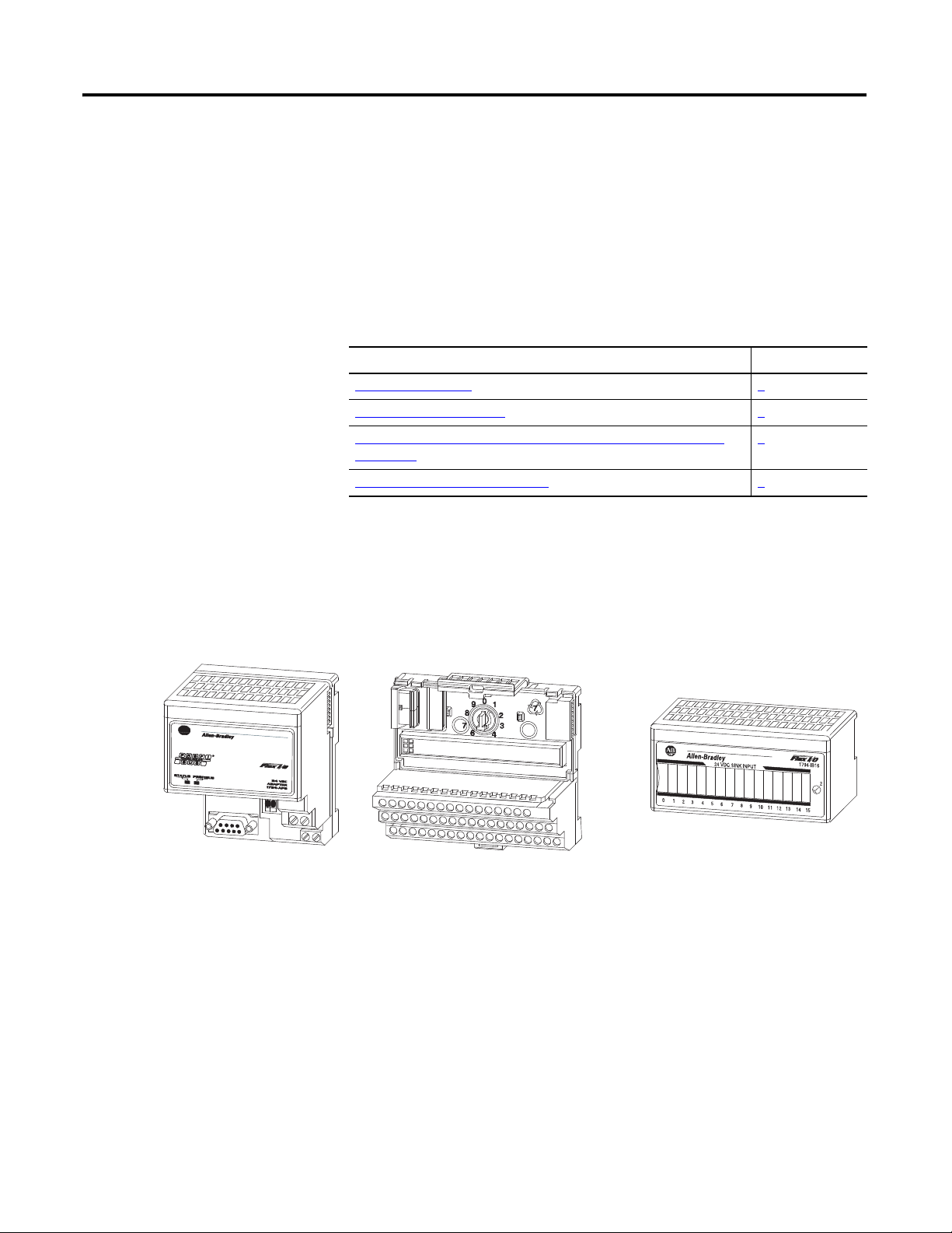
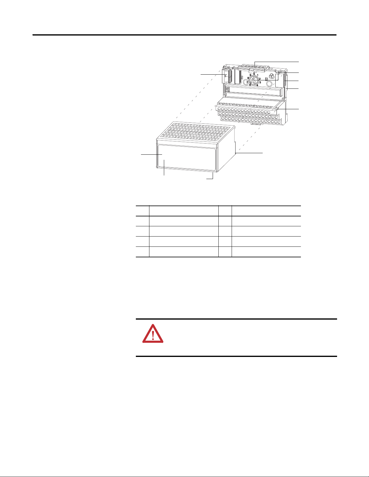
Chapter
I/O moduleTerminal base
20125
Adapter
1
Overview of FLEX I/O and Your Analog Module
Overview
The FLEX I/O System
Read this chapter to familiarize yourself with configurable features on the FLEX
I/O High Density modules. The following table lists where to find specific
information in this chapter.
Topic Page
The FLEX I/O System
Types of FLEX I/O Modules 2
How FLEX I/O Analog Modules Communicate with Programmable
Controllers
Physical Features of Your Modules 4
FLEX I/O is a small, modular I/O system for distributed applications that
performs all of the functions of rack-based I/O. The FLEX I/O system contains
the following components shown below:
1
3
• adapter/power supply – powers the internal logic for as many as eight I/O
modules
• terminal base – contains a terminal strip to terminate wiring for two- or
three-wire devices
• I/O module – contains the bus interface and circuitry needed to perform
1 Publication 1794-UM062A-EN-P - September 2012
specific functions related to your application
Page 10
2 Overview of FLEX I/O and Your Analog Module
Types of FLEX I/O Modules
The following FLEX I/O analog modules are described in this user manual:
FLEX I/0 Analog Modules
Catalog Number Voltage Inputs Outputs Description
1794-IE8 24V DC 8 — analog – 8 input, single-ended,
1794-IE8XT
1794-IE12 24V DC 12 — analog – 12 input, single-ended,
1794-OE4 24V DC — 4 analog – 4 output, single-ended,
1794-OE4XT
1794-OE12 24V DC — 12 analog – 12 output, single-ended,
1794-IE4XOE2 24V DC 4 2 analog – 4 input, single-ended,
1794-IE4XOE2XT
1794-IE8XOE4 24V DC 8 4 analog – 8 input, single-ended,
(1)
Modules with "XT" indicated in the catalog number signify extended temperature modules.
(1)
(1)
(1)
non-isolated
non-isolated
non-isolated
non-isolated
non-isolated and 2 output,
single-ended, non-isolated
non-isolated and 4 output,
single-ended, non-isolated
FLEX I/O analog input, output and combination modules are block transfer
modules that interface analog signals with any Allen-Bradley programmable
controllers that have block transfer capability. Block transfer programming moves
input from the module’s memory to a designated area in the processor data table,
and output data words from a designated area in the processor data table to the
module’s memory. Block transfer programming also moves configuration words
from the processor data table to module memory.
The analog modules have selectable ranges as shown in the table below:
Analog Module Selectable Ranges
Voltage Current
0…10V DC 0…20 mA
+/- 10V DC 4…20 mA
Publication 1794-UM062A-EN-P - September 2012
Page 11
Overview of FLEX I/O and Your Analog Module 3
ADAPTER
ACTIVE
FAULT
LOCAL
FAULT
24VDC
POWER SUPPLY
RIO ADAPTER
1794-ASB
IN 0 IN 2 IN 4 IN 6IN 1 IN 3 IN 5 IN 7
TC RTD INPUT 8 CHANNEL
3
1794-IRT8
PWR
FF F F F F FF
45316
The adapter transfers your configuration data.
FlexBus
External devices transmit
analog signals to the module.
The module converts
analog signals into binary
format and stores these
values until the adapter
requests their transfer.
The adapter receives data
from the modules and stores
it in the data table.
The adapter module determine that the
transfer was made without error and
input values are within specified range.
Your ladder program can use and/or move the data (if valid)
before it is written over by the transfer of new data in a
subsequent transfer.
1
4
5
6
2
3
New configuration data can be sent to the
module any time during operation.
7
1794-ACN15
1794-ACNR15
1794-ADN
1794-AENT
1794-AENTR
MicroLogix
1794-ASB
1794-APB
Adapter
1794-AENT shown
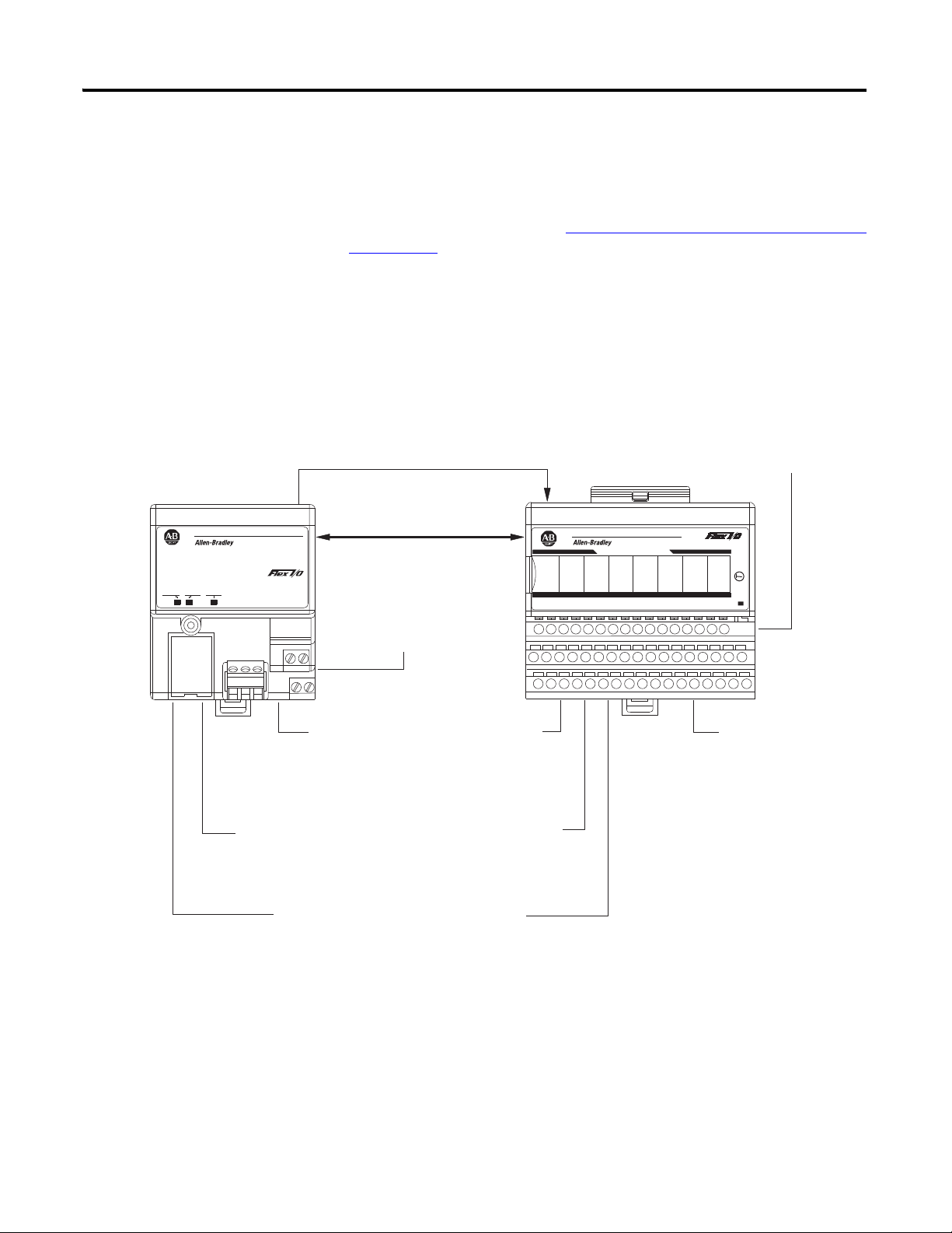
How FLEX I/O Analog
Modules Communicate
with Programmable
Controllers
The adapter/power supply transfers data to the module (block transfer write) and
from the module (block transfer read) using BTW and BTR instructions in your
ladder diagram program. These instructions let the adapter obtain input values
and status from the module, and let you send output values and establish the
module’s mode of operation. The Typical Communication Between the Adapter
and a Module figure describes the communication process.
Typical Communication Between the Adapter and a Module
Publication 1794-UM062A-EN-P - September 2012
Page 12
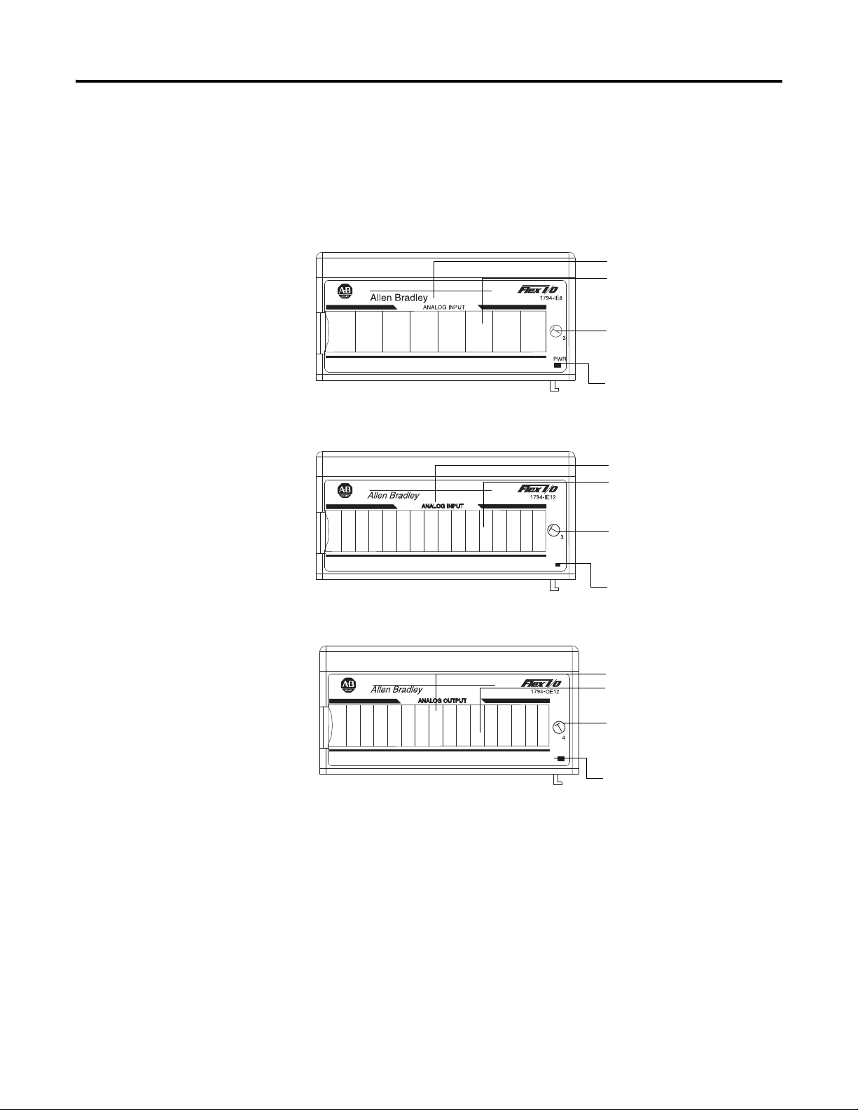
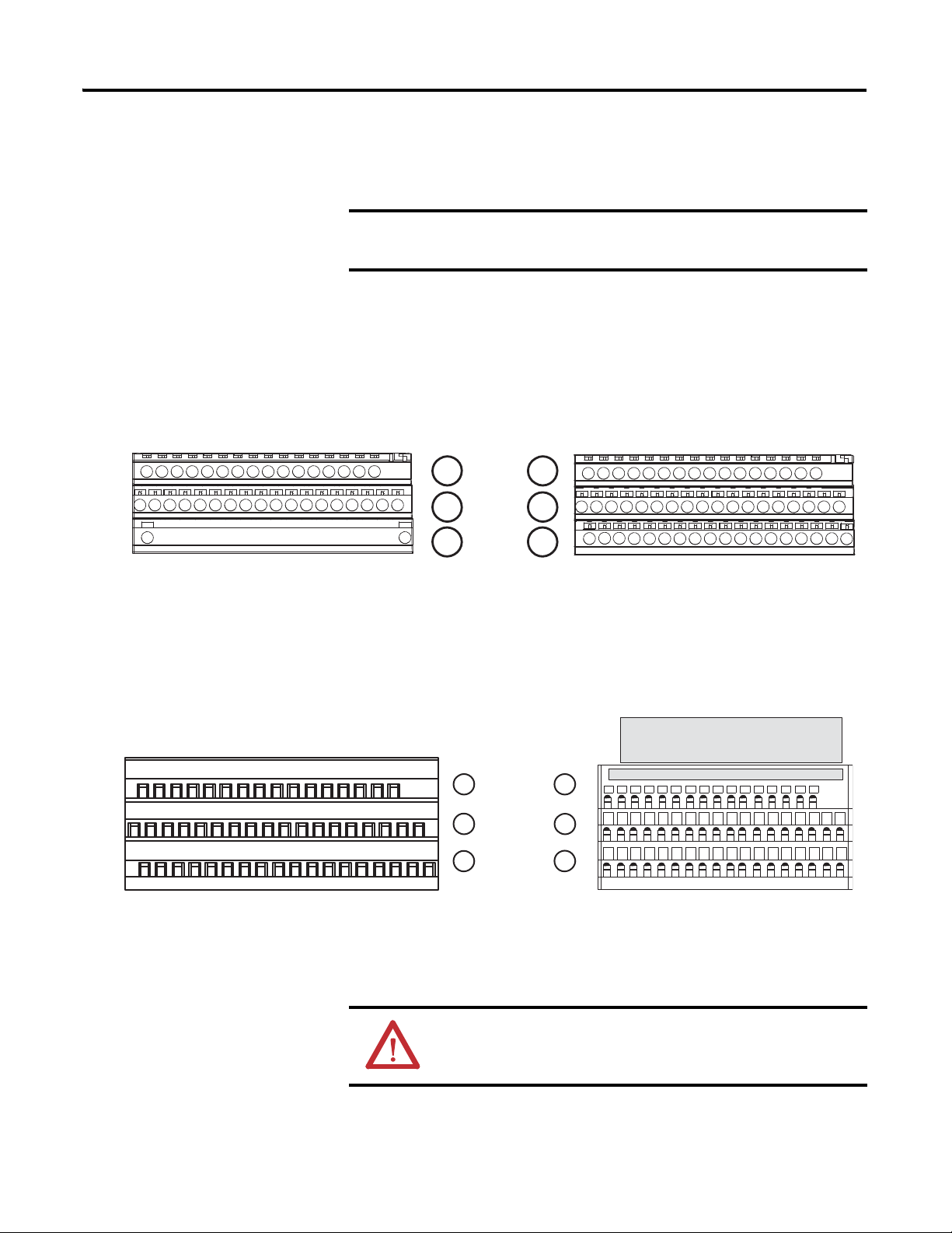
4 Overview of FLEX I/O and Your Analog Module
1794-IE8 (1794-IE8XT)
1794-IE12
1794-OE12
OK
-
-
OK
Module type
Removable label
Keyswitch
position indicator (#3)
Power on indicator
Module type
Removable label
Keyswitch
position indicator (#3)
Power on indicator
Module type
Removable label
Keyswitch
position indicator (#4)
Power on indicator
46060
Physical Features of Your Modules
The module label identifies the keyswitch position, wiring and module type. A
removable label provides space for writing individual designations per your
application. Indicators are provided to identify input fault conditions, and to
show when power is applied to the module.
Module Labels and Indicators
Publication 1794-UM062A-EN-P - September 2012
Page 13
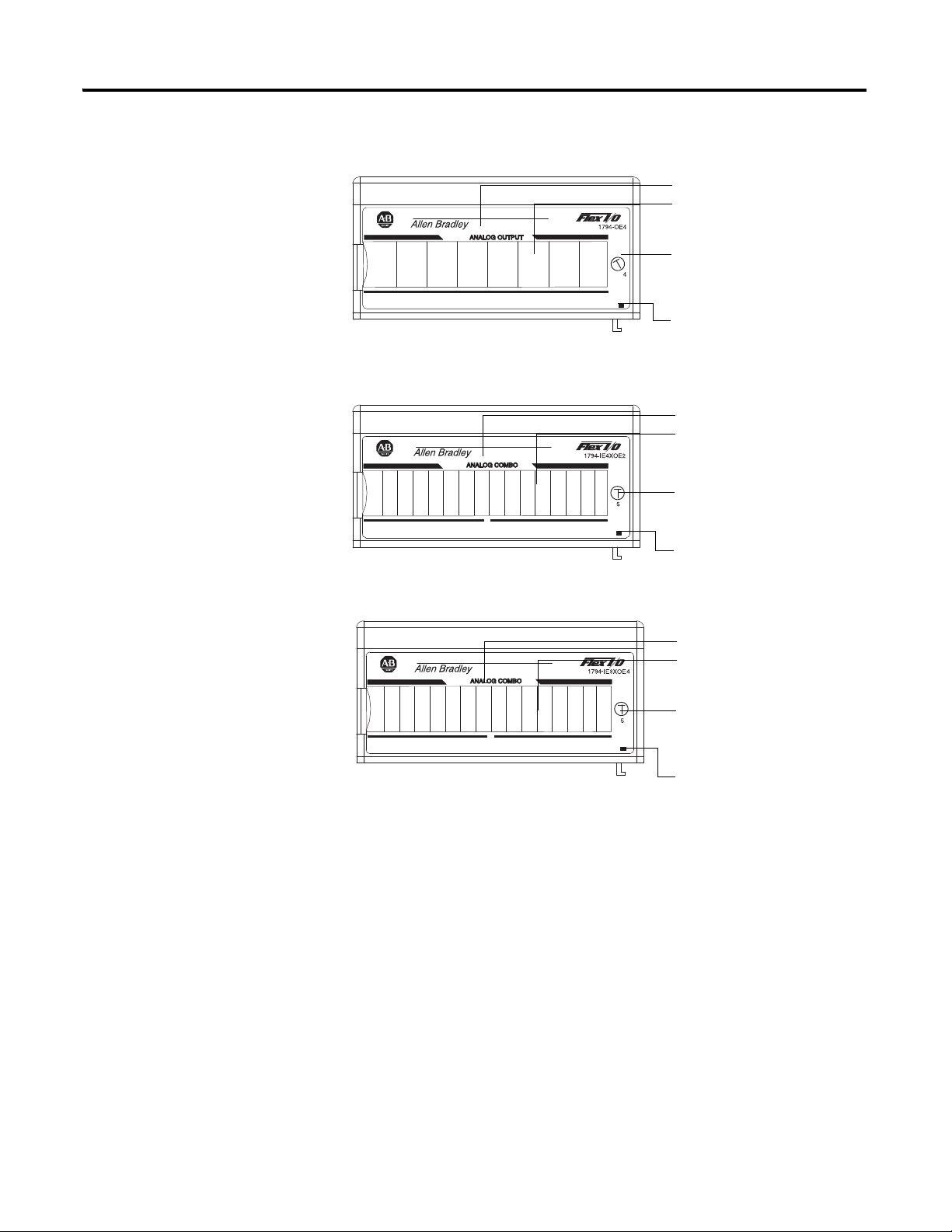
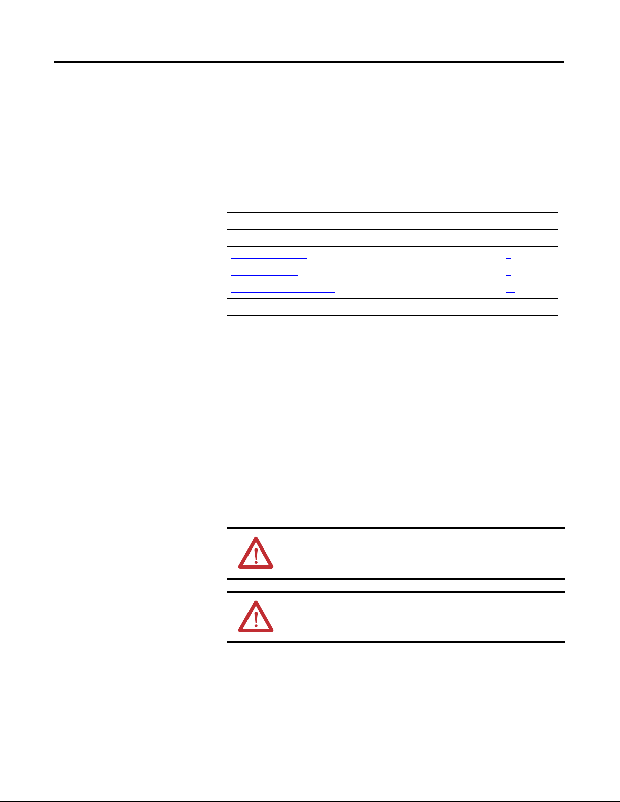
Overview of FLEX I/O and Your Analog Module 5
1794-OE4 (1794-OE4XT)
1794-IE4XOE2 (1794-IE4XOE2XT)
1794-IE8XOE4
-
OK
-
OK
-
OK
Module type
Removable label
Keyswitch
position indicator (#5)
Power on indicator
Module type
Removable label
Keyswitch
position indicator (#5)
Power on indicator
46061
Output designators
Module type
Removable label
Keyswitch
position indicator (#4)
Power on indicator
Summary
In this chapter you learned about the FLEX I/O system and the types of analog
modules and how they communicate with programmable controllers.
Publication 1794-UM062A-EN-P - September 2012
Page 14

6 Overview of FLEX I/O and Your Analog Module
Notes:
Publication 1794-UM062A-EN-P - September 2012
Page 15
Install Your FLEX I/O Module
Chapter
2
Overview
Before You Install Your Module
This chapter provides you with pre-installation requirements and instructions on
how to install your FLEX I/O analog module.
Topic Page
Before You Install Your Module
Power Requirements 7
Install the Module 9
Wire the Terminal Base Unit 15
Connect Wiring to the FLEX I/O Module 16
Before installing your FLEX I/O analog module, you need to:
• Calculate the power requirements of all modules in each chassis,
• verify that a suitable enclosure is available for installation of the module,
and
• position the keyswitch on the terminal base.
7
Power Requirements
7 Publication 1794-UM062A-EN-P - September 2012
The wiring of the terminal base unit is determined by the current draw through
the terminal base. Make certain that the current draw does not
exceed 10 A.
ATTENTION: Total current draw through the terminal base unit is
limited to 10 A. Separate power connections may be necessary.
ATTENTION: Do not daisy chain power or ground from the terminal
base unit to any AC or DC digital module terminal base unit.
Page 16
8 Install Your FLEX I/O Module
Digital Input
Module
Analog
Module
Analog
Module
Analog
Module
Digital Output
Module
Digital Input
Module
TC/RTD/mV
Module
Analog
Module
TC/RTD/mV
Module
TC/RTD/mV
Module
TC/RTD/mV
Module
TC/RTD/mV
Module
Daisychain
Individual
Combination
24V DC
24V DC
24V DC
24V DC
24V DC
24V DC
45318
Wiring when total current draw is less than 10A
Wiring when total current draw is less than 10A
Total current draw through any base unit must not be greater than 10A
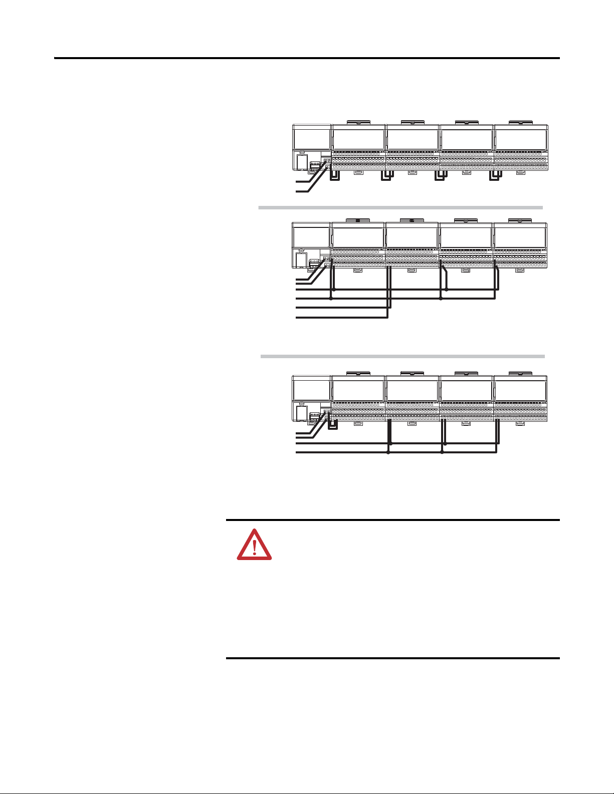
Methods of wiring the terminal base units are shown in the illustration below.
ATTENTION: Note the following rules for each type of wiring
configuration:
• Daisychain – AIl modules must be analog or TC/RTD/mV modules
for this configuration.
• Individual – Use this type of configuration for any noisy DC digital
I/O modules in your system.
• Combination – All modules powered by the same power supply
must be analog modules for the combination type of
configuration.
Publication 1794-UM062A-EN-P - September 2012
Page 17
Install Your FLEX I/O Module 9
1
2
3
4
6
7
7
8
9
0
45319
Install the Module
Installation of the analog module consists of:
• mounting the terminal base unit
• installing the analog module into the terminal base unit
• installing the connecting wiring to the terminal base unit
If you are installing your module into a terminal base unit that is already installed,
proceed to the section, Mount the Analog Module on the Terminal Base Unit
page 13
.
, on
Mount on a DIN Rail
ATTENTION: Do not remove or replace a terminal base unit when
power is applied. Interruption of the FlexBus can result in
unintended operation or machine motion.
Install the Terminal Base Unit
1. Remove the cover plug in the male connector of the unit to which you are
connecting this terminal base unit.
2. Check to make sure that the 16 pins in the male connector on the adjacent
device are straight and in line so that the mating female connector on this
terminal base unit will mate correctly.
Make certain that the female FlexBus connector is fully retracted into the
base unit.
Publication 1794-UM062A-EN-P - September 2012
Page 18
10 Install Your FLEX I/O Module
45320
45321
3. Position the terminal base at a slight angle and hooked over the top of the
35 x 7.5 mm DIN rail A (Allen Bradley part number 199-DR1; 46277-3).
0
9
1
8
7
6
7
2
3
4
4. Slide the terminal base over tight against the adapter (or proceeding
terminal base). Make sure the hook on the terminal base slides under the
edge of the adapter (or proceeding terminal base) and the FlexBus
connector is fully retracted.
5. Rotate the terminal base onto the DIN rail with the top of the rail hooked
under the lip on the rear of the terminal base.
Use caution to make sure that the female FlexBus connector does not strike
any of the pins in the mating male connector.
6. Press down on the terminal base unit to lock the terminal base on the DIN
rail. If the terminal base does not lock into place, use a screwdriver or
similar device to open the locking tab, press down on the terminal base
until flush with the DIN rail and release the locking tab to lock the base in
place.
Publication 1794-UM062A-EN-P - September 2012
Page 19
Install Your FLEX I/O Module 11
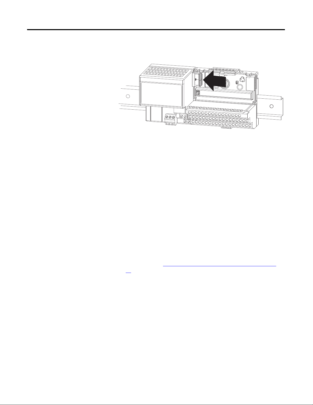
45322
Gently push the FlexBus connector into the side of the adapter (or
proceeding terminal base) to complete the backplane connection.
0
9
1
8
7
6
7
2
3
4
For specific wiring information, refer to the installation instructions for
the module you are installing in this terminal base unit.
7. Repeat the above steps to install the next terminal base unit.
Ensure that the cover of the FlexBus connector on the last terminal base
unit is in place.
Mount on a Panel or Wall
Installation of a FLEX I/O system on a wall or panel consists of:
• laying out the drilling points on the wall or panel.
• drilling the pilot holes for the mounting screws.
• mounting the adapter mounting plate.
• installing the terminal base units and securing them to the wall or panel.
If you are installing your module into a terminal base unit that is already installed,
proceed to the section, Mount the Analog Module on the Terminal Base Unit
page 13
.
, on
Publication 1794-UM062A-EN-P - September 2012
Page 20
12 Install Your FLEX I/O Module
1
2
3
4
45323
millimeter
(inch)
45327
Use the mounting kit Cat. No. 1794-NM1 for panel/wall mounting.
1.4
(35.5)
0
9
1
8
7
6
7
2
3
4
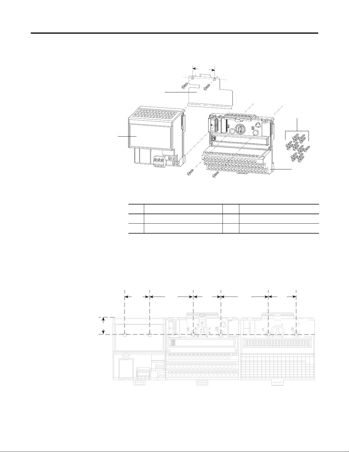
Description Description
1 Mounting plate for adapter 3 Terminal base unit (not included)
2 #6 Self-tapping screws 4 Adapter module (not included)
To install the mounting plate on a wall or panel:
1. Lay out the required points on the wall/panel as shown in the drilling
dimension drawing.
Drilling Dimensions for Panel or Wall Mounting of FLEX I/O
Millimeters
(Inches)
35.5
(1.4)
58.5
(2.3)
35.5
(1.4)
58.5
(2.3)
21 (0.83)
35.5
(1.4)
Publication 1794-UM062A-EN-P - September 2012
2. Drill the necessary holes for the #6 self-tapping mounting screws.
Page 21

Install Your FLEX I/O Module 13
IMPORTANT
3. Mount the mounting plate for the adapter module using two #6
self-tapping screws (18 included for mounting up to 8 modules and the
adapter).
Make certain that the mounting plate is properly grounded to the
panel. Refer to Industrial Automation Wiring and Grounding
Guidelines, publication 1770-4.1
.
4. Hold the adapter at a slight angle and engage the top of the mounting plate
in the indention on the rear of the adapter module.
5. Press the adapter down flush with the panel until the locking lever locks.
6. Position the terminal base unit up against the adapter and push the female
bus connector into the adapter.
7. Secure to the wall with two #6 self-tapping screws.
8. Repeat for each remaining terminal base unit.
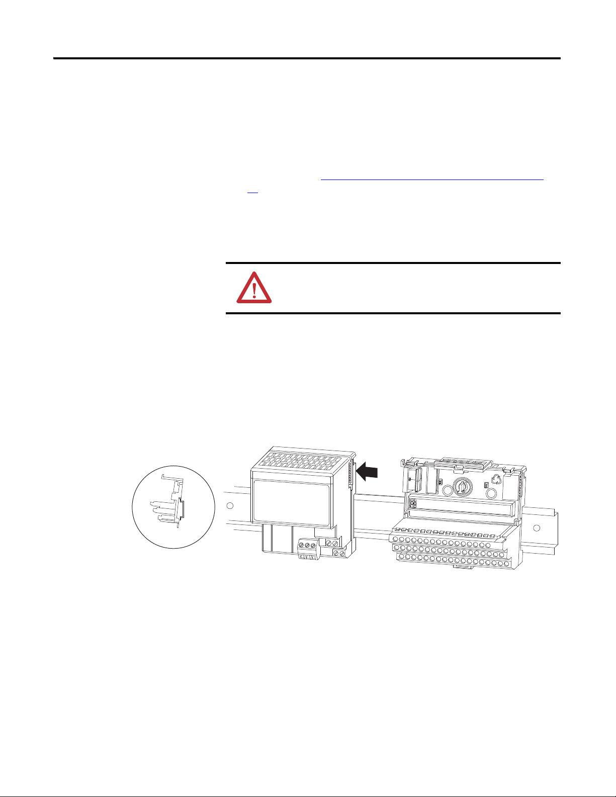
Mount the Analog Module on the Terminal Base Unit
The analog module mounts on a 1794-TBx terminal base unit. More specific
terminal bases, see Module and Terminal Base Unit Compatibility
1. Rotate keyswitch (3) on terminal base unit (4) clockwise to the position
required for your module, see table Keyswitch Positions for Your Module
on page 13.
Do not change the position of the keyswitch after wiring the terminal base
unit.
Keyswitch Positions for Your Module
Module Keyswitch Position
1794-IE8 3
1794-IE8XT
1794-IE12
1794-OE12 4
1794-OE4
1794-OE4XT
1794-IE4XOE2 5
1794-IE4XOE2XT
on page 16.
1794-IE8XOE4
Publication 1794-UM062A-EN-P - September 2012
Page 22
14 Install Your FLEX I/O Module
1
2
3
4
5
6
7
8
Label here or under here
40231
Description Description
1 FlexBus connector 5 Base unit
2 Latching mechanism 6 Alignment groove
3 Keyswitch 7 Alignment bar
4 Cap plug 8 Module
2. Make certain the FlexBus connector (1) is pushed all the way to the left to
connect with the neighboring terminal base or adapter.
You cannot install the module unless the connector is fully extended.
3. Make sure the pins on the bottom of the module are straight so they will
align properly with the connector in the terminal base unit.
ATTENTION: If you remove or insert the module while the backplane
power is on, an electrical arc can occur. This could cause an explosion
in hazardous location installations. Be sure that power is removed or
the area is nonhazardous before proceeding.
4. Position the module (8) with its alignment bar (7) aligned with the groove
(6) on the terminal base.
Publication 1794-UM062A-EN-P - September 2012
5. Press firmly and evenly to seat the module in the terminal base unit.
The module is seated when the latching mechanism is locked into the
module.
Page 23
Install Your FLEX I/O Module 15
IMPORTANT
1794-TB2
1794-TB3
A
B
C
0...15
34, 51
16...33
A
B
C
34 and 50 = 24V DC
35 and 51 = common
16, 33 = chassis ground
45328
34 and 50 = 24V DC
35 and 51 = common
16, 33, 38 = chassis ground
40…45, 47 = chassis ground
0123456789101112131415
16 17 18 19 20 21 22 23 24 25 26 27 28 29 30 31 32 33
34 35 36 37 38 39 40 41 42 43 44 45 46 47 48 49 50 51
A
B
C
A
B
C
1794-TB3G
1794-TB3GS
0...15
34...51
16...33
0 1 2 3 4 5 6 7 8 9 101112131415
18 19 20 21 22 23 3324 25 26 27 28 29 30 31 3217
35 36 37 38 47 48 49 5034 51
16
39 40 41 42 43 44 45 46
Label placed at top of wiring area
34 and 50 = 24V DC
35 and 51 = common
16 and 33 = chassis ground
40…45 = chassis ground
35 and 51 = common
34 and 50 = 24V DC
16 and 33 = chassis ground
40…45 = chassis ground
45328
6. Remove cap plug and attach another terminal base unit to the right of this
terminal base unit if required.
Make sure the last terminal base has the cap plug in place.
The adapter is capable of addressing eight modules. Do not exceed a
maximum of eight terminal base units in your system.
Wire the Terminal Base Unit
Wiring to the analog modules is made through the terminal base unit on which
the module mounts.
1794-TB2 and 1794-TB3 Wiring
1794-TB3G and 1794-TB3GS Wiring
ATTENTION: Total current draw through the terminal base unit is
limited to 10A. Separate power connections to the terminal base unit
may be necessary.
Publication 1794-UM062A-EN-P - September 2012
Page 24
16 Install Your FLEX I/O Module
Connect Wiring to the FLEX I/O Module
Module and Terminal Base Unit Compatibility
Module 1794-TB2 1794-TB3 1794-TB3S 1794-TB3G 1794-TB3GS 1794-TB3T 1794-TB3TS TBN
1794-IE8 Yes Yes No No No No No No
1794-IE8XT Yes Yes Yes No No Yes Yes No
1794-IE12 No No No Yes Yes No No No
1794-OE12 No No No Yes Yes No No No
1794-OE4 Yes Yes No No No No No No
1794-OE4XT Yes Yes Yes No No Yes Yes Yes
1794-IE4XOE2 Yes Yes No No No No No No
1794-IE4XOE2XT Yes Yes Yes No No Yes Yes No
1794-IE8XOE4 No No No Yes Yes No No No
Wiring to the analog module is made through the terminal base unit on which
the module mounts.
Verify which terminal base units your module is compatible with in table Module
and Terminal Base Unit Compatibility on page 16.
Connect Wiring Using a 1794-TB2 or 1794-TB3 Terminal Base Unit
1. Connect the individual signal wiring to numbered terminals on the 0…15
row (A) on the terminal base unit. Use Belden 8761 cable for signal wiring.
ATTENTION: Connect only one current or one voltage signal per
channel. Do not connect both current and voltage on one channel.
2. Connect each channel signal return to:
• 1794-IE8 – the associated terminal on row (B).
• 1794-OE4 – the corresponding terminal on the same row (A).
• 1794-IE4XOE2 – inputs: the associated terminal on row (B); outputs:
the corresponding terminal on the same row (A).
3. Connect +24V DC to designated terminals on the 34…51 row (C), and
24V common to designated terminals on the 16…33 row (B).
ATTENTION: To reduce susceptibility to noise, power analog
modules and discrete modules from separate power supplies. Do
not exceed a length of 10 m (33 ft) for power cabling.
Publication 1794-UM062A-EN-P - September 2012
If daisy chaining the +24V DC power to the next base unit, connect a jumper
from terminal 51 on this base unit to terminal 34 on the next base unit. Connect
Page 25
Install Your FLEX I/O Module 17
the 24V DC common/return from terminal 33 on this base unit to terminal 16
on the next base unit.
Wire Connections for 1794-TB2, and 1794-TB3 using the 1794-IE8 Module
Channel Signal Type Label
Markings
1794-TB2 and 1794-TB3
Input Common Terminal
Input 0 Current I A-0 B-17
Voltage V A-1 B-18
Input 1 Current I A-2 B-19
Voltage V A-3 B-20
Input 2 Current I A-4 B-21
Voltage V A-5 B-22
Input 3 Current I A-6 B-23
Voltage V A-7 B-24
Input 4 Current I A-8 B-25
Voltage V A-9 B-26
Input 5 Current I A-10 B-27
Voltage V A-11 B-28
Input 6 Current I A-12 B-29
Voltage V A-13 B-30
Input 7 Current I A-14 B-31
Voltage V A-15 B-32
24V DC common
B-16…33
(1)
+24V DC power 1794-TB2 – C-34…51
1794-TB3 – C-34…51
(1)
Terminals 16…33 are internally connected in the terminal base unit.
Wire Connections for 1794-TB2, and 1794-TB3 using the 1794-OE8 Module
Channel Signal Type Label
Markings
1794-TB2 and 1794-TB3
Output
Output 1 Current signal I A-0
Current common RET
A-1
(1)
Voltage signal V A-2
Voltage common RET
A-3
(1)
Current signal I A-4
Current common RET
A-5
(1)
Voltage signal V A-6
Voltage common RET
Publication 1794-UM062A-EN-P - September 2012
A-7
(1)
Page 26

18 Install Your FLEX I/O Module
Wire Connections for 1794-TB2, and 1794-TB3 using the 1794-OE8 Module
Channel Signal Type Label
Markings
Current signal I A-8
Current common RET
Voltage signal V A-10
Voltage common RET
Current signal I A-12
Current common RET
Voltage signal V A-14
Voltage common RET
24V DC common
+24V 1794-TB2 – C-34…51
1794-TB3 – C-34…51
(1)
Terminals 1, 3, 5, 7, 9, 11, 13 and 15 are connected in the terminal base unit.
(2)
Terminals 16…33 are internally connected in the terminal base unit.
1794-TB2 and 1794-TB3
Output
(1)
A-9
(1)
A-11
(1)
A-13
(1)
A-15
B-16…33
(2)
Publication 1794-UM062A-EN-P - September 2012
Page 27

Install Your FLEX I/O Module 19
Wire Connections for 1794-TB2, and 1794-TB3 using the 1794-IE4XOE2 Module
Channel Signal Type Label
Markings
1794-TB2 and 1794-TB3
Signal Common Terminal
Input 0 Current I 0 17
Voltage V 1 18
Input 1 Current I 2 19
Voltage V 3 20
Input 2 Current I 4 21
Voltage V 5 22
Input 3 Current I 6 23
Voltage V 7 24
Output 0 Current signal I 8
Current common RET
(2)
9
Voltage signal V 10
Voltage common RET
11
(2)
Output 1 Current signal I 12
Current common V
13
(2)
Voltage signal I 14
Voltage common V
24V DC Common
16…33
(1)
15
(2)
+24V DC Power 1794-TB2 – 34…51
1794-TB3 – 34…51
(1)
Terminals 16…33 are internally connected in the terminal base unit.
(2)
Terminals 9, 11, 13, and 15 are internally connected in the module to 24V DC common.
Connect Wiring Using a 1794-TB3G or 1794-TB3GS Terminal Base Unit
1. Connect individual signal wiring to numbered terminals on 0…15 row
(A), and 17…32 row (B) for 1794-TB3G and 1794-TB3GS as indicated in
the following tables.
2. Connect any signal wiring shields to functional ground as near as possible
to the module.
1794-TB3G and 1794-TB3GS only: Connect to earth ground terminals
B16, B33, C38, C40…C45 and C47.
3. Connect the -V DC common (return) to terminal 35 on the 34…51
row (C).
Publication 1794-UM062A-EN-P - September 2012
Page 28

20 Install Your FLEX I/O Module
4. If daisy chaining +V power to the next terminal base unit, connect a
jumper from terminal 50 (+VDC power) on this base unit to the +VDC
terminal on the next terminal base unit, and connect a jumper from
terminal 51 (-VDC common) on this base unit to the common terminal
on the next terminal base unit.
5. If continuing -V common to the next terminal base unit, connect a jumper
from terminal 51 (-VDC common) on this base unit to the to the common
terminal on the next terminal base unit.
Wire Connections for 1794-TB3G, and 1794-TB3GS using the 1794-IE12 Module
Channel Signal Type Label
Markings
Input 0 Current I A-0 B-17
Voltage V A-1
Input 1 Current I A-2 B-18
Voltage V A-3
Input 2 Current I A-4 B-23
Voltage V A-5
Input 3 Current I A-6 B-24
Voltage V A-7
Input 4 Current I A-8 B-25
Voltage V A-9
Input 5 Current I A-10 B-26
Voltage V A-11
Input 6 Current I A-12 B-31
Voltage V A-13
Input 7 Current I A-14 B-32
Voltage V A-15
1794-TB3G and 1794-TB3GS
Input Common Terminal
Publication 1794-UM062A-EN-P - September 2012
Input 8 Current I B-19 C-37
Voltage V B-20
Input 9 Current I B-21 C39
Voltage V B-22
Input 10 Current I B-27 C-46
Voltage V B-28
Input 11 Current I B-29 C-48
Voltage V B-30
Page 29

Install Your FLEX I/O Module 21
Wire Connections for 1794-TB3G, and 1794-TB3GS using the 1794-IE12 Module
Channel Signal Type Label
Markings
24V DC common
1794-TB3G – C-35, C-51
1794-TB3G and 1794-TB3GS
Input Common Terminal
(1)
1794-TB3GS – C-35, C-51
+24V DC power
1794-TB3G – C-34, C-50
(2)
1794-TB3GS – C-34, C-50
Chassis ground
(Shield)
(1)
Terminals C-35 and C-51 are internally connected in the terminal base unit.
(2)
Terminals C-34 and C-50 are internally connected in the terminal base unit.
(3)
Terminals B-16, B-33, C-38, C-40 through C- 45, and C-47 are internally connected to chassis ground
1794-TB3G – B-16, B-33, C-38, C-40…45, C-47
1794-TB3GS – B-16, B-33, C-38, C-40…45, C-47
Wire Connections for 1794-TB3G, and 1794-TB3GS using the 1794-OE12 Module
Channel Signal Type Label
Markings
Output 0 Current I A-0 B-17
Voltage V A-1
Output 1 Current I A-2 B-18
1794-TB3G and 1794-TB3GS
Output Common Terminal
(3)
Voltage V A-3
Output 2 Current I A-4 B-23
Voltage V A-5
Output 3 Current I A-6 B-24
Voltage V A-7
Output 4 Current I A-8 B-25
Voltage V A-9
Output 5 Current I A-10 B-26
Voltage V A-11
Output 6 Current I A-12 B-31
Voltage V A-13
Output 7 Current I A-14 B-32
Voltage V A-15
Output 8 Current I B-19 C-37
Voltage V B-20
Output 9 Current I B-21 C39
Voltage V B-22
Publication 1794-UM062A-EN-P - September 2012
Page 30

22 Install Your FLEX I/O Module
Wire Connections for 1794-TB3G, and 1794-TB3GS using the 1794-OE12 Module
Channel Signal Type Label
Markings
1794-TB3G and 1794-TB3GS
Output Common Terminal
Output 10 Current I B-27 C-46
Voltage V B-28
Output 11 Current I B-29 C-48
Voltage V B-30
24V DC common
1794-TB3G – C-35, C-51
(1)
1794-TB3GS – C-35, C-51
+24V DC power
1794-TB3G – C-34, C-50
(2)
1794-TB3GS – C-34, C-50
Chassis ground
(Shield)
(1)
Terminals C-35 and C-51 are internally connected in the terminal base unit.
(2)
Terminals C-34 and C-50 are internally connected in the terminal base unit.
(3)
Terminals B-16, B-33, C-38, C-40 through C- 45, and C-47 are internally connected to chassis ground
1794-TB3G – B-16, B-33, C-38, C-40…45, C-47
1794-TB3GS – B-16, B-33, C-38, C-40…45, C-47
Wire Connections for 1794-TB2, and 1794-TB3 using the 1794-IE8XOE4 Module
(3)
Channel Signal Type Label
Marking
1794-TB3G or 1794-TB3GS
Input/Output Common Terminal
Input 0 Current I0 A-0 B-17
Voltage V0 A-1
Input 1 Current I1 A-2 B-18
Voltage V1 A-3
Input 2 Current I2 A-4 B-23
Voltage V2 A-5
Input 3 Current I3 A-6 B-24
Voltage V3 A-7
Input 4 Current I4 A-8 B-25
Voltage V4 A-9
Input 5 Current I5 A-10 B-26
Voltage V5 A-11
Input 6 Current I6 A-12 B-31
Voltage V6 A-13
Input 7 Current I7 A-14 B-32
Voltage V7 A-15
Publication 1794-UM062A-EN-P - September 2012
Page 31

Install Your FLEX I/O Module 23
Wire Connections for 1794-TB2, and 1794-TB3 using the 1794-IE8XOE4 Module
Channel Signal Type Label
Marking
Output 0 Current I8 B-19 C-37
Voltage V8 B-20
Output 1 Current I9 B-21 C-39
Voltage V9 B-22
Output 2 Current I10 B-27 C-46
Voltage V10 B-28
Output 3 Current I11 B-29 C-48
Voltage V11 B-30
-V DC Common 1794-TB3G and 1794-TB3GS – Terminals C-35 and C-51 are internally
connected in the terminal base unit.
+V DC Power 1794-TB3G and 1794-TB3GS –Terminals C-34 and C-50 are internally
connected in the terminal base unit.
Chassis
Ground (Shield)
1794-TB3G and 1794-TB3GS – Terminals B-16, B-33, C-38, C-40
through C- 45, and C-47 are internally connected to chassis ground.
1794-TB3G or 1794-TB3GS
Input/Output Common Terminal
Connect Wiring Using a 1794-TB3S, 1794-TB3T, 1794-TB3TS, or 1794-TBN Terminal Base Unit
1. Connect individual input/output wiring to numbered terminals on the
0…15 row (A) for 1794-TB3S, 1794-TB3T and 1794-TB3TS, or on row
(B) for the 1794-TBN as indicated in the following tables.
2. Connect channel common/return to the associated terminal on row (A)
or row (B) for the 1794-TB3S, 1794-TB3T and 1794-TB3TS, or on
row (C) for the 1794-TBN. For input devices requiring terminal base
power, connect the channel power wiring to the associated terminal on
row (C).
3. Connect any signal wiring shields to functional ground as near as possible
to the module.
1794-TB3T or -TB3TS only: Connect to earth ground terminals
C-39…C-46.
4. Connect the +V DC power to terminal 34 on the 34…51 row (C) and -V
common/return to terminal 16 on the (B) row.
5. If daisychaining +V power to the next terminal base, connect a jumper
from terminal 51 (+V DC) on this base unit to terminal 34 on the next
base unit.
Publication 1794-UM062A-EN-P - September 2012
Page 32

24 Install Your FLEX I/O Module
Wire Connections for 1794-TB3S, 1794-TB3T and 1794-TB3TS using the 1794-IE8XT Module
6. If continuing DC common (-V) to the next base unit, connect a jumper
from terminal 33 (common) on this base unit to terminal 16 on the next
base unit.
Channel Signal Type Label
Markings
1794
-TB3S,
-TB3T,
1794-TB3S 1794-TB3S 1794
-TB3T
-TB3TS
-TB3TS
Input
Power
(1)
Common Terminal Shield
Input 0 Current I A-0 C-35 B-17 B-17 C-39
Voltage V A-1 C-36 B-18
Input 1 Current I A-2 C-37 B-19 B-18 C-40
Voltage V A-3 C-38 B-20
Input 2 Current I A-4 C-39 B-21 B-21 C-41
Voltage V A-5 C-40 B-22
Input 3 Current I A-6 C-41 B-23 B-23 C-42
Voltage V A-7 C-42 B-24
Input 4 Current I A-8 C-43 B-25 B-25 C-43
Voltage V A-9 C-44 B-26
Input 5 Current I A-10 C-45 B-27 B-27 C-44
Voltage V A-11 C-46 B-28
Input 6 Current I A-12 C-47 B-29 B-29 C-45
Voltage V A-13 C-48 B-30
Input 7 Current I A-14 C-49 B-31 B-31 C-46
Voltage V A-15 C-50 B-32
24V DC
common
1794-TB3S – Terminals 16…33 are internally connected in the terminal base unit.
1794-TB3T, 1794TB3TS- – Terminals 16, 17, 19, 21, 23, 25, 27, 29, 31 and 33 are internally
connected in the terminal base unit.
+24V DC
power
1794-TB3S – Terminals 34…51 are internally connected in the terminal base unit.
1794-TB3T, 1794-TB3TS – Terminals 34, 35, 50 and 51 are internally connected in the terminal
base unit.
Chassis
1794-TB3T, 1794-TB3TS – Terminals 39…46 are internally connected to chassis ground.
ground
(Shield)
(1)
Use when transmitter requires terminal base power.
Publication 1794-UM062A-EN-P - September 2012
Page 33

Install Your FLEX I/O Module 25
Wire Connections for 1794-TB3S, 1794-TB3T and 1794-TB3TS using the 1794-OE8XT
Module
Channel Signal Type Label
Markings
1794-TB3S, 1794-TB3T,
1794-TB3TS
Output
Terminal
(1)
Shield
1794-TB3T,
1794-TBN
Output
Term in al
1794-TB3TS
Output 0 Current I A-0 C-39 B-0
Current I RET A-1 C-1
Voltage V A-2 C-40 B-2
Voltage V RET A-3 C-3
Output 1 Current I A-4 C-41 B-4
Current I RET A-5 C-5
Voltage V A-6 C-42 B-6
Voltage V RET A-7 C-7
Output 2 Current I A-8 C-43 B-8
Current I RET A-9 C-9
Voltage V A-10 C-44 B-10
Voltage V RET A-11 C-11
Output 3 Current I A-12 C-45 B-12
Current I RET A-13 C-13
(2)
Voltage V A-14 C-46 B-14
Voltage V RET A-15 C-15
24V DC
common
1794-TB3S – Terminals 16…33 are internally connected in the terminal base
unit.
1794-TB3T, 1794TB3TS- – Terminals 16, 17, 19, 21, 23, 25, 27, 29, 31 and 33
are internally connected in the terminal base unit.
+24V DC
power
1794-TB3S – Terminals 34…51 are internally connected in the terminal base
unit.
1794-TB3T, 1794-TB3TS – Terminals 34, 35, 50 and 51 are internally
connected in the terminal base unit.
Chassis
ground
1794-TB3T, 1794-TB3TS – Terminals 39…46 are internally connected to
chassis ground.
(Shield)
(1)
1A-1, 3, 5, 7, 9, 11, 13 and 15 are internally connected in the module to 24V DC common.
(2)
2C-1, 3, 5, 7, 9, 11, 13 and 15 are internally connected in the module to 24V DC common
Publication 1794-UM062A-EN-P - September 2012
Page 34

26 Install Your FLEX I/O Module
Wire Connections for 1794-TB3S, 1794-TB3T and 1794-TB3TS using the 1794-IE4XOE2XT Module
Channel Signal
Ty pe
Label
Markings
1794
-TB3S,
1794-TB3S 1794-TB3S 1794-TB3T,
1794-TB3TS
-TB3T,
-TB3TS
Input/Output
Term in al
(1)
Power
Terminal
Common Terminal Shield
(2)
Input 0 Current I A-0 C-35 B-17 B-17 C-39
Voltage V A-1 C-36 B-18
Input 1 Current I A-2 C-37 B-19 B-18 C-40
Voltage V A-3 C-38 B-20
Input 2 Current I A-4 C-39 B-21 B-21 C-41
Voltage V A-5 C-40 B-22
Input 3 Current I A-6 C-41 B-23 B-23 C-42
Voltage V A-7 C-42 B-24
Output 0 Current I A-8
C-43
Voltage RET A-9
VA-10 C-44
RET A-11
Output 1 Current I A-12 C-45
Voltage RET A-13
VA-14 C-46
24V DC
common
+24V DC
power
Chassis
ground
(Shield)
(1)
(2)
Chapter Summary
RET A-15
1794-TB3S – Terminals 16…33 are internally connected in the terminal base unit.
1794-TB3T, 1794TB3TS- – Terminals 16, 17, 19, 21, 23, 25, 27, 29, 31 and 33 are internally
connected in the terminal base unit.
1794-TB3S – Terminals 34…51 are internally connected in the terminal base unit.
1794-TB3T, 1794-TB3TS – Terminals 34, 35, 50 and 51 are internally connected in the terminal
base unit.
1794-TB3T, 1794-TB3TS – Terminals 39…46 are internally connected to chassis ground.
A-9, 11, 13 and 15 are internally connected in the module to 24V DC common.
Use when transmitter requires terminal base power.
In this chapter you learned how to install the FLEX I/O analog module in an
existing programmable controller system and how to wire to a terminal base unit.
Publication 1794-UM062A-EN-P - September 2012
Page 35

Chapter
3
Write Configuration to and Read Status from Your Module
Overview
Configure Your Analog Module
This chapter describes how to configure, read data from, and map data to your
FLEX I/O analog module.
Topic Page
Configure Your Analog Module
Range Selection 28
Safe State Value Selection 28
Data Format 28
Read Data From Your Module 28
Map Data for the Module 29
Because of the many analog devices available and the wide variety of possible
configurations, you must configure your module to conform to the analog device
and specific application that you have chosen. The module is configured using a
group of data table words that are transferred to the module using a block transfer
write instruction.
The software configurable features available are:
• input/output range selection
• safe state operating value (customer selected analog values the module will
maintain in the event of a network communication error)
27
ATTENTION: PLC-5 family programmable controllers that use 6200
software programming tools can take advantage of the IOCONFIG
utility to configure these modules. IOCONFIG uses menu-based
screens for configuration without having to set individual bits in
particular locations. Refer to your 6200 software literature for details.
Page 36

28 Write Configuration to and Read Status from Your Module
Range Selection
Individual input channels are configurable to operate with the following voltage
or current ranges.
Voltage and Current Ranges
Ranges Bit Settings
Configure Select Full Range
0…10V DC / 0…20 mA 0 1
4…20 mA 1 0
-10…+10V DC 1 1
(1)
Off
(1)
When configured to OFF, individual output channels drive 0V or 0 mA.
ATTENTION: If using Series A modules, do not use configure select
and full range bit settings of 0. Individual channels revert to 4…20
mA with bit selections of all zeroes. This could result in unwanted or
incorrect action.
00
You can select individual channel ranges using the designated words of the write
block transfer instruction. See the Word/Bit Descriptions for your particular
module for word and bit numbers.
Safe State Value Selection
Data Format
Read Data From Your Module
You can select the analog values that your output module maintains in the event
of a network communication error. When the multiplex control bits (M) are
cleared simultaneously by a communication error, (or by the user), the analog
outputs automatically switch to the values set in the safe state analog words. This
allows you to define a safe operating state for controlled devices which depend on
the analog output from the module.
The data returned from the analog-to-digital converter in the module is 12-bit
resolute. This value is left-justified into a 16-bit field, reserving the most
significant bit for a sign bit. The 4…20 mA mode scales in the module and uses all
16 bits.
For more information on values for various current and voltage modes, and an
example of scaling to engineering terms, see Module Programming
on page 67.
Read programming transmits status and data from the analog module to the
processor data table in one I/O scan. The processor user program initiates the
request to the transfer data from the analog module to the processor.
Publication 1794-UM062A-EN-P - September 2012
Page 37

Write Configuration to and Read Status from Your Module 29
Map Data for the Module
Chapter Summary
Read and write words and bit/word descriptions describe the information
written to and read from the analog modules. Each word is composed of 16 bits.
For a complete list of data for your specific module, see Data Tables
In this chapter you learned about data and instructions to configure and map
your FLEX I/O High-Density Analog Modules.
on page 43.
Publication 1794-UM062A-EN-P - September 2012
Page 38

30 Write Configuration to and Read Status from Your Module
Notes:
Publication 1794-UM062A-EN-P - September 2012
Page 39

Communicate With Your Module
1123
16-point Discrete Input Module
Chapter
4
Overview
About DeviceNet Manager
Communication Over the I/O Backplane
Read this chapter to familiarize yourself with configurable features on the input
and output analog modules
For Information About See Page
About DeviceNet Manager
Communication Over the I/O Backplane 31
Polled I/O Structure 32
Defaults 33
DeviceNet Manager is a software tool used to configure your FLEX I/O
DeviceNet adapter and its related modules. This software tool can be connected
to the adapter via the DeviceNet network.
You must know and understand how DeviceNet Manager works in order to add a
device to the network. Refer to the DeviceNet Manager software online help for
more information on using DeviceNet Manager software.
A FLEX I/O adapter communicates to other network system components over
the network. The adapter communicates with its I/O modules over the
backplane.
31
The I/O map for a module is divided into read words and write words. Read
words consist of input and status words, and write words consist of output and
configuration words. The number of read words or write words can be 0 or more.
The length of each I/O module’s read words and write words vary in size
depending on module complexity. Each I/O module will support at least 1 input
word or 1 output word. Status and configuration are optional, depending on the
module.
For example, a 16 point discrete input module will have up to 2 read words and 1
write word.
Delay
Delay
Time
Time
Check the I/O map for each module for the exact mapping.
Page 40

32 Communicate With Your Module
46062
15Bit: 01234567810 through 15
I/O Module Fault Bits
Node Address Changed Bit
Slot 0
Slot 1
Slot 2
Slot 3
Slot 4
Slot 5
Slot 6
Slot 7
9
I/O State Bit
Not Used
46063
Polled I/O Structure
Output data is received by the adapter in the order of the installed I/O modules.
The Output data for Slot 0 is received first, followed by the Output data for Slot
1, and so on up to slot 7.
The first word of input data sent by the adapter is the Adapter Status Word. This
is followed by the input data from each slot, in the order of installed I/O
modules. The Input data from Slot 0 is first after the status word, followed by
Input data from Slot 2, and so on to slot 7.
Network
Network WRITE
READ
FLEX I/O adapter
Read data
Adapter
status
Slot 0 input data
Slot 1 input data
...
Slot 7 input data
Write data
Slot 0 output data
Slot 1 output data
...
Slot 7 output data
...
...
Read
Write
I/O module
slot 0
I/O module
slot 1
...
I/O module
slot 7
Adapter Input Status Word
The input status word consists of:
• I/O module fault bits — 1 status bit for each slot
• node address changed — 1 bit
• I/O status — 1 bit
Publication 1794-UM062A-EN-P - September 2012
Page 41

Communicate With Your Module 33
The adapter input status word bit descriptions are shown in table Word Bit
Description on page 33.
Word Bit Description
Bit Description Bit Explanation
I/O module fault 0 This bit is set (1) when an error is detected in slot position 0.
1 This bit is set (1) when an error is detected in slot position 1.
2 This bit is set (1) when an error is detected in slot position 2.
3 This bit is set (1) when an error is detected in slot position 3.
4 This bit is set (1) when an error is detected in slot position 4.
5 This bit is set (1) when an error is detected in slot position 5.
6 This bit is set (1) when an error is detected in slot position 6.
7 This bit is set (1) when an error is detected in slot position 7.
Defaults
Node address
changed
I/O state 9 Bit = 0 – idle
8 This bit is set (1) when the node address switch setting has
been changed since power up.
Bit = 1 – run
10…15 Not used – sent as zeroes.
Possible causes for an I/O module fault are:
• transmission errors on the FLEX I/O backplane
•a failed module
• a module removed from its terminal base
• incorrect module inserted in a slot position
•the slot is empty
The node address changed bit is set when the node address switch setting has
been changed since power up. The new node address does not take effect until
the adapter has been powered down and then powered back up. Until this power
cycling occurs, the node address switches will not match the actual node address.
Each I/O module has default values associated with it. At default, each module
generates inputs/status and expects outputs/configuration.
Module Default Values
Module Defaults for: Factory Defaults Real Time Size
Catalog
Number
1794-IE8/B 8-pt Analog Input 9 6 8 0
1794-IE8XT 8-pt Analog Input 9 6 8 0
1794-IE12 12-pt Analog Input 13 2 12 1
1794-OE4/B 4-pt Analog Output 1 14 0 4
Publication 1794-UM062A-EN-P - September 2012
Description Input
Default
Output
Default
Input
Default
Output
Default
Page 42

34 Communicate With Your Module
Module Default Values
Module Defaults for: Factory Defaults Real Time Size
Catalog
Number
1794-OE4XT 4-pt Analog Output 1 14 0 4
1794-OE12 12-pt Analog Output 1 14 0 13
1794-IE4XOE2 4 in/2 out Analog Combo 5 10 4 2
1794-IE4XOE2XT 4 in/2 out Analog Combo 5 10 4 2
1794-IE8XOE4 8 in/4 out Analog Combo 9 6 8 5
Description Input
Default
Output
Default
Input
Default
Output
Default
Factory defaults are the values assigned by the adapter when you:
• first power up the system, and
• no previous stored settings have been applied.
For analog modules, the defaults reflect the actual number of input words/output
words. For example, for the 8 input analog module, you have 9 input words, and 6
output words.
Chapter Summary
You can change the I/O data size for a module by reducing the number of words
mapped into the adapter module, as shown in real time size.
Real time size is the setting that provides optimal real time data to the adapter
module.
Analog modules have 15 words assigned to them. This is divided into inputs
words and output words. You can reduce the I/O data size to fewer words to
increase data transfer over the backplane. For example, an 8 input analog module
has 9 words input and 6 words output with factory default. You can reduce the
input words to 8 by not using the underrange settings set in Word 9. Likewise,
you can reduce the write words to 0, thus eliminating the configuration setting
and unused words.
For information on using DeviceNet Manager software, refer to the DeviceNet
Manager Software help.
This chapter explained how to communicate with your module.
Publication 1794-UM062A-EN-P - September 2012
Page 43

Specifications
Appendix A
Overview
This Appendix lists all input, output, general and environment specifications, as
well as certifications for the following FLEX I/O Analog Modules: 1794-IE8,
1794-IE8XT, 1794-IE12, 1794-OE4, 1794-OE4XT, 1794-OE12,
1794-IE4XOE2, 1794-IE4XOE2XT, 1794-IE8XOE4.
Input Specifications
The following are input specifications for the FLEX I/O analog input and
combination modules.
Input Specifications – 1794-IE8, 1794-IE8XT, 1794-IE12, 1794-IE4XOE2, 1794-IE4XOE2XT, 1794-IE8XOE4 Analog Input Modules
Specification 1794-IE12 1794-IE8XOE4 1794-IE8, 1794-IE8XT 1794-IE4XOE2,
1794-IE4XOE2XT
Number of inputs 12 single-ended,
non-isolated
Resolution
Voltage
Current
Conversion type Successive approximation
Conversion rate, all
channels
Input current terminal
(user configurable)
Input voltage terminal
(user configurable)
320 μV/cnt
0.641 μA/cnt
8.0 ms 256 μs
4…20 mA
0…20 mA
±10V
0…10V
8 single-ended, non-isolated 4 single-ended,
non-isolated
2.56 mV/cnt unipolar; 5.13 mV/cnt bipolar
5.13 μA/cnt
Normal mode rejection
ratio
voltage terminal
current terminal
Step response to 63%
voltage terminal
current terminal
35 Publication 1794-UM062A-EN-P - September 2012
-3 db @ 0.05 Hz; -20 db/decade
-52 db @ 50 Hz: -54 db @ 60 Hz
-3 db @ 1.5 Hz: -20 db/decade
-29 db @ 50 H
1.3 s
0.09 s
-3 db @ 17 Hz; -20 db/decade
-10.0 dB @ 50 Hz, -11.4 dB @ 60 Hz
-3 db @ 9 Hz; -20 db/decade
-15.3 dB @ 50 Hz, -16.8 dB @ 60 Hz
9.4 ms
18.2 ms
Page 44

36 Specifications
Input Specifications – 1794-IE8, 1794-IE8XT, 1794-IE12, 1794-IE4XOE2, 1794-IE4XOE2XT, 1794-IE8XOE4 Analog Input Modules
Specification 1794-IE12 1794-IE8XOE4 1794-IE8, 1794-IE8XT 1794-IE4XOE2,
1794-IE4XOE2XT
Input Impedance
Voltage Terminal
Current Terminal
> 1 MΩ
< 100 Ω
(1)
238 Ω
100 kΩ
Absolute accuracy
Voltage Terminal
Current Terminal
0.1% Full scale @ 25 °C
0.1% Full scale @ 25 °C
0.29% Full scale @ 25 °C
0.29% Full scale @ 25 °C
Accuracy Drift with
Temperature
Voltage Terminal
Current Terminal
0.00428% Full scale/°C
0.00407% Full scale/°C
Max overload 30V continuous or 32 mA continuous,
one channel at a time
(1)
If 24V DC is removed from the module, input resistance is <100 Ω. This is also true at 0 mA current input, even if there is 24V DC. If there is an input current applied, input
resistance is >1 M
Ω.
Output Specifications
The following are output specifications for the FLEX I/O analog output and
combination modules.
Output Specifications – 1794-OE4, 1794-OE4XT, 1794-OE12, 1794-IE4XOE2, 1794-IE4XOE2XT, 1794-IE8XOE4
Specification 1794-OE12 1794-IE8XOE4 1794-OE4, 1794-OE4XT 1794-IE4XOE2,
1794-IE4XOE2XT
Number of outputs 12 single-ended,
non-isolated
Output voltage range, nom ±10V
Output current, max 0…20 mA
Voltage output current
3 mA
load, max
Voltage resolution 320 μV/cnt 2.56 μV/cnt
Current resolution 0.641 μA/cnt 5.13 μA/cnt
Absolute accuracy
Voltage Terminal
Current Terminal
0.1% Full scale @ 25%
0.1% Full scale @ 25%
Accuracy Drift with
Temperature
Voltage Terminal
Current Terminal
0.004% Full scale/° C
0.004% Full scale/° C
Resistive load, mA output 0…750 Ω @ 24V DC 15…750 Ω @ 24V DC
4 single-ended, non-isolated 2 single-ended,
non-isolated
0.133% Full scale @ 25%
0.425% Full scale @ 25%
0.0045% Full scale/° C
0.0069% Full scale/° C
Publication 1794-UM062A-EN-P - September 2012
Page 45

General Specifications
The following are general specifications common to all the FLEX I/O analog
modules in this publication.
Output Specifications – 1794-OE4, 1794-OE4XT, 1794-OE12, 1794-IE4XOE2, 1794-IE4XOE2XT, 1794-IE8XOE4
Specifications 37
Specification 1794-IE12, 1794-OE12,
1794-IE8XOE4
Module location 1794-TB3G
1794-TB3GS
Keyswitch position 1794-IE12
3
1794-OE12
4
1794-IE8XOE4
5
Dimensions, approx.
(HxWxD)
Calibration None required
Indicators 1 green/red power/status indicator 1 green power indicator
Data format 16 bit 2’s complement, left justified
External DC power supply,
nom
94.0 x 94.0 x 53.3 mm
(3.7 x 3.7 x 2.1 in.)
24V DC
1794-IE8, 1794-IE8XT, 1794-OE4, 1794-OE4XT,1794-IE4XOE2,
1794-IE4XOE2XT
1794-TB2
1794-TB3
1794 -TB3S
1794-TB3T
1794-TB3TS
For 1794-OE4, 1794-OE4XT only
1794-TBN
1794-IE8, 1794-IE8XT
3
1794-OE4, 1794-OE4XT
4
1794-IE4XOE2, 1794-IE4XOE2XT
5
45.7 x 94.0 x 53.3 mm
(1.8 x 3.7 x 2.1 in.)
External DC power supply,
voltage range
External DC power supply,
current
FlexBus current 80 mA 70 mA
Isolation voltage 50V continuous
10.0…31.2V DC
(includes 5% AC ripple)
1794-IE12
30 mA @ 24V DC; 45 mA @ 10V DC
1794-OE12
320 mA @ 24V DC; 720 mA @ 10V DC
1794-IE8XOE4
140 mA @ 24V DC; 280 mA @ 10V DC
Tested at 850V DC for 60 s between
user power to system
No isolation between individual
channels
Publication 1794-UM062A-EN-P - September 2012
19.2…31.2V DC
(includes 5% AC ripple)
70 mA @ 24V DC
1794-IE8, 1794-IE8XT
60 mA @ 24V DC
60 mA – For 1794-IE8, 1794-IE8XT only
50V continuous
Tested @ 850V DC for 1 s between user power to system
No isolation between individual channels
150 mA @ 12V DC
Page 46

38 Specifications
Output Specifications – 1794-OE4, 1794-OE4XT, 1794-OE12, 1794-IE4XOE2, 1794-IE4XOE2XT, 1794-IE8XOE4
Specification 1794-IE12, 1794-OE12,
1794-IE8XOE4
Power dissipation, max. 1794-IE12
1.2 W @ 31.2V DC
1.1 W @ 24V DC
0.9 W @ 10.0V DC
1794-IE8, 1794-IE8XT, 1794-OE4, 1794-OE4XT,1794-IE4XOE2,
1794-IE4XOE2XT
1794-IE8
4.0 W @ 31.2V DC
3.0 W @ 31.2V DC
1794-OE8
4.5 W @ 31.2V DC
1794-OE12
4.0 W @ 31.2V DC
4.3 W @ 24V DC
4.0 W @ 10.0V DC
1794-IE8XOE4
3.0 W @ 31.2V DC
2.3 W @ 24V DC
2.0 W @ 10.0V DC
Thermal dissipation, max. 1794-IE12
4.1 BTU/hr @ 31.2V DC
1794-OE12
4.7 BTU/hr @ 24V DC
1794-IE8
10.2 BTU/hr @ 31.2V DC
1794-OE8
15.3 BTU/hr @ 31.2V DC
13.6 BTU/hr @ 31.2V DC
1794-IE8XOE4
10.3 BTU/hr @ 31.2V DC
Wire size – Power 0.34…2.5 mm2 (22…12 AWG) stranded copper wire rated at 75° C 167° F) or higher
4 mm2 (12 gauge) stranded, max – For 1794-IE8 and 1794-IE8XT only
1.2 mm (3/64 in.) insulation, max.
Wire category
(1)
2 – on signal port
2 – on power ports
Terminal base screw
torque
1794-TB3G and 1794-TB3GS
0379…1.02 Nm (7…9 lb-in.)
0.8 Nm (7 lb-in.)
1794-TBN
1.0 Nm (9 lb-in.)
Enclosure type rating None (open-style)
(1)
Use this Conductor Category information for planning conductor routing. Refer to Industrial Automation Wiring and Grounding Guidelines, publication 1770-4.1.
Publication 1794-UM062A-EN-P - September 2012
Page 47

Environmental Specifications
The following are the environmental specifications common to all the FLEX I/O
analog modules in this publication.
Environmental Specifications
Specification Description
Temperature, operating IEC 60068-2-1 (Test Ad, Operating Cold),
IEC 60068-2-2 (Test Bd, Operating Dry Heat),
IEC 60068-2-14 (Test Nb, Operating Thermal Shock):
0…55 °C (32…131 °F)
-20…60 °C (-40…185 °F) – For 1794-IE12, 1794-OE12 and 1794-IE8XOE4 only
Temperature, nonoperating IEC 60068-2-1 (Test Ab, Unpackaged Nonoperating Cold),
IEC 60068-2-2 (Test Bb, Unpackaged Nonoperating Dry Heat),
IEC 60068-2-14 (Test Na, Unpackaged Nonoperating Thermal Shock):
–40…85 °C (–40…185 °F)
Relative humidity IEC 60068-2-30 (Test Db, Unpackaged Damp Heat):
5…95% noncondensing
Vibration IEC 60068-2-6 (Test Fc, Operating):
5 g @ 10…500 H
Shock, operating IEC60068-2-27 (Test Ea, Unpackaged shock):
Operating 30 g
Specifications 39
Shock, nonoperating IEC60068-2-27 (Test Ea, Unpackaged shock):
Nonoperating 50 g
Emissions CISPR 11:
Group 1, Class A
ESD immunity IEC 61000-4-2:
6 kV contact discharges
4 kV contact discharges – For 1794-IE8, 1794-OE4, 1794-IE4XOE2 and 1794-IE4XOE2XT only
8 kV air discharges
Radiated RF immunity 1794-IE12, 1794-OE12, 1794-IE8XOE4
IEC 61000-4-3:
10 V/m with 1 kHz sine-wave 80% AM from 30…2000 MHz
10 V/m with 200 Hz 50% pulse 100% AM at 900 MHz
10 V/m with 200 Hz 50% pulse 100% AM at 1890 MHz
3 V/m with 1 kHz sine-wave 80% AM from 2…2.7 GHz
1794-IE8, 1794-OE4, 1794-IE4XOE2 and 1794-IE4XOE2XT
10V/m with 1kHz sine-wave 80%AM from 30MHz to 1000MHz
EFT/B immunity IEC 61000-4-4:
±2 kV at 5 kHz on power ports – For 1794-IE12, 1794-OE12, 1794-IE8XOE4 only
±2 kV at 5 kHz on signal ports
Publication 1794-UM062A-EN-P - September 2012
Page 48

40 Specifications
Environmental Specifications
Specification Description
Conducted RF immunity 1794-IE12, 1794-OE12, 1794-IE8XOE4
IEC 61000-4-6:
10V/m with 1kHz sine-wave 80%AM from 150 kHz…80 MHz
1794-IE8, 1794-OE4, 1794-IE4XOE2 and 1794-IE4XOE2XT
IEC 61000-4-6:
10V/m with 1kHz sine-wave 80%AM from 150 kHz…30 MHz
Surge transient immunity IEC 6100-4-5:
±2 kV line-earth (CM) on shielded ports – For 1794-IE8, 1794-OE4, 1794-IE4XOE2 and
1794-IE4XOE2XT only
Certification
The following are the certifications common to all the FLEX I/O analog
modules in this publication.
Certifications
Certifications (when
product is marked)
Value
(1)
c-UL-us UL Listed Industrial Control Equipment, certified for US and
Canada. See UL File E65584
UL Listed for Class I, Division 2 Group A,B,C,D Hazardous
Locations, certified for U.S. and Canada. See UL File E194810.
CSA CSA certified Process Control Equipment
CSA certified for Class 1, Division 2, Groups A, B, C and D
Hazardous locations
CE European Union 2004/108/EC EMC Directive, compliant with:
EN 61326; Meas./Control/Lab., Industrial Requirements
EN 61000-6-2; Industrial Immunity
EN 61000-6-4; Industrial Emissions
EN 50082-2; Industrial Immunity
C-Tick Australian Radiocommunications Act, compliant with:
AS/NZS CISPR 11; Industrial Emissions
Ex European Union 94/9/EC ATEX Directive, compliant with:
EN 60079-15; Potentially Explosive Atmospheres, Protection
"n" (Zone 2)
(1)
1) See the Product Certification link at www.ab.com for Declarations of Conformity, Certificates, and other
certification details.
Publication 1794-UM062A-EN-P - September 2012
Page 49

Differences Between Series
Appendix B
Overview
The following lists major differences between series A and series B of your
FLEX I/O analog modules.
.
Differences Between Series A and Series B
Catalog Number Description Series A Series B
1794-IE8
1794-OE4
1794-IE4XOE2
Specifications
1794-OE4 Output current terminal 4 mA output until module is configured
1794-IE4XOE2 Output current terminal 4 mA output until module is configured
1794-IE8
1794-OE4
1794-IE4XOE2
Power Up bit in Read
Word
Change to range selection
tables
Output voltage terminal 2V output until module is configured
Output voltage terminal 2V output until module is configured
Agency Certification
(when product or
packaging
is marked)
None This bit is set when all bits in the
No off position available. Module
produces either 2V or 4 mA, depending
on the range selected, until module is
configured.
4…20 mA user configurable
0…20 mA user configurable
±10V user configurable
0…10V user configurable
4…20 mA user configurable
0…20 mA user configurable
±10V user configurable
0…10V user configurable
•CSA certified
•CSA Class I, Division 2, Groups A, B, C,
D certified
•UL listed
configuration register are 0
unconfigured state).
Off position now produces 0V or 0 mA
depending on the range selected, until
module is configured.
0 mA output until module is configured
4…20 mA user configurable
0…20 mA user configurable
0 V output until module is configured
±10V user configurable
0…10V user configurable
0 mA output until module is configured
4…20 mA user configurable
0…20 mA user configurable
0 V output until module is configured
±10V user configurable
0…10V user configurable
•CSA certified
•CSA Class I, Division 2, Groups A, B, C, D
certified
•UL listed
•CE marked for all applicable directives
41 Publication 1794-UM062A-EN-P - September 2012
Page 50

42 Differences Between Series
Notes:
Publication 1794-UM062A-EN-P - September 2012
Page 51

Data Tables
Appendix C
Overview
I/O messages are sent to (consumed) and received from (produced) the FLEX
I/O modules. These messages are mapped into the processor memory. This
appendix lists the default data maps for 1794 FLEX I/O analog modules.
For the default data map of See page
1794-IE8 Series B and 1794-IE8XT – 8 Input Analog Module
Image Table Mapping
1794-IE12 – 12 Input Analog Module Image Table Mapping 47
1794-OE4 Series B and 1794-OE4XT– 4 Output Analog Module
Image Table Mapping
1794-OE12 – 12 Output Analog Module Image Table Mapping 54
1794-IE4XOE2 Series B and 1794-IE4XOE2XT – 4 Input 2
Output Analog Combo Module Image Table Mapping
1794-IE8XOE4 – 8 Input 4 Output Analog Combo Module Image
Table Mapping
44
51
57
61
Block Transfer Read and Write
The following block transfer read and write word bit information is presented for
experienced users only.
43 Publication 1794-UM062A-EN-P - September 2012
Page 52

44 Data Tables
Module Image
I/O Image
Input Data Channel 0
Input Data Channel 1
Input Data Channel 2
Input Data Channel 3
Input Data Channel 4
Input Data Channel 5
Input Data Channel 6
Input Data Channel 7
Underrange
Configure select
Not used
Not used
Not used
Not used
Not used
Input S ize
Output S ize
0 or 1 W ord
1 to 9 W ords
PU
46064
1794-IE8 Series B and 1794-IE8XT – 8 Input Analog Module Image Table Mapping
Memory Map – 1794-IE8/B and 1794-IE8XT Analog Input Module
Decimal Bit15 1413 1211 1009080706050403020100Size
Octal Bit 17 1615 1413 1211100706050403020100Read/Write Words
S Analog Value Channel 0 Read Word 0
S Analog Value Channel 1 Read Word 1
S Analog Value Channel 2 Read Word 2
S Analog Value Channel 3 Read Word 3
S Analog Value Channel 4 Read Word 4
S Analog Value Channel 5 Read Word 5
S Analog Value Channel 6 Read Word 6
S Analog Value Channel 7 Read Word 7
PU Not used – set to zero U7 U6 U5 U4 U3 U2 U1 U0 Read Word 8
C7 C6 C5 C4 C3 C2 C1 C0 F7 F6 F5 F4 F3 F2 F1 F0 Write Word 0
Not used Write Word 1…5
Where: PU = Power up bit – included in series B modules only.
U = Underrange bits for 4…20 mA inputs
C = Configure select bit
F = Full range bit
S = sign bit (in 2’s complement)
Publication 1794-UM062A-EN-P - September 2012
Page 53

Data Tables 45
Range Selection Bits – 1794-IE8/B and 1794-IE8XT Analog Input Module
Channel No. Ch 00 Ch 01 Ch 02 Ch 03 Ch 04 Ch 05 Ch 06 Ch 07
F0 C0 F1 C1 F2 C2 F3 C3 F4 C4 F5 C5 F6 C6 F7 C7
Bit 00 08
0…10V DC
1010101010101010
(10)
01 09
(11)
02 10
(12)
03 11
(13)
04 12
(14)
05 13
(15)
06 14
(16)
07 15
(17)
/0…20 mA
4…20 mA 0101010101010101
-10…+10V DC 1111111111111111
Off
(1)
0000000000000000
Where: C = Configure select bit
F = Full range bit
(1)
When configured to OFF, individual channels will return 000H on Series B modules, and 4…20 mA on Series A modules.
Word/Bit Descriptions – 1794-IE8/B and 1794-IE8XT Analog Input Module
Word Decimal Bit
Definition
(Octal Bit)
Read Word 0 Bits 00…14
(00…16)
Channel 0 analog data – 12-bit left justified two's
complement number; unused lower bits are zero;
4…20 mA uses all 16 bits.
Bit 15 (17) Channel 0 analog data sign bit.
Read word 1 Bits 00…14
(00…16)
Channel 1 analog data – 12-bit left justified two's
complement number; unused lower bits are zero;
4…20 mA uses all 16 bits.
Bit 15 (17) Channel 1 analog data sign bit.
Read word 2 Bits 00…14
(00…16)
Bit 15 (17) Channel 2 analog data sign bit.
Read word 3 Bits 00…14
(00…16)
Bit 15 (17) Channel 3 analog data sign bit.
Read word 4 Bits 00…14
(00…16)
Bit 15 (17) Channel 4 analog data sign bit.
Read word 5 Bits 00…14
(00…16)
Bit 15 (17) Channel 5 analog data sign bit.
Channel 2 analog data – 12-bit left justified two's
complement number; unused lower bits are zero;
4…20 mA uses all 16 bits.
Channel 3 analog data – 12-bit left justified two's
complement number; unused lower bits are zero;
4…20 mA uses all 16 bits.
Channel 4 analog data – 12-bit left justified two's
complement number; unused lower bits are zero;
4…20 mA uses all 16 bits.
Channel 5 analog data – 12-bit left justified two's
complement number; unused lower bits are zero;
4…20 mA uses all 16 bits.
Publication 1794-UM062A-EN-P - September 2012
Page 54

46 Data Tables
Word/Bit Descriptions – 1794-IE8/B and 1794-IE8XT Analog Input Module
Word Decimal Bit
Definition
(Octal Bit)
Read word 6 Bits 00…14
(00…16)
Channel 6 analog data – 12-bit left justified two's
complement number; unused lower bits are zero;
4…20 mA uses all 16 bits.
Bit 15 (17) Channel 6 analog data sign bit.
Read word 7 Bits 00…14
(00…16)
Channel 7 analog data – 12-bit left justified two's
complement number; unused lower bits are zero;
4…20 mA uses all 16 bits.
Bit 15 (17) Channel 7 analog data sign bit.
Read word 8 Bits 00…07 Underrange bits (U) for individual channels (4…20
mA current input only) – Bit 00 corresponds to input
channel 0, bit 01 corresponds to input channel 1, and
so on. When set (1), indicates either a broken or open
input wire, or input current at or below 4 mA.
Bits 08…14
Not used – set to 0.
(10…16)
Bit 15 (17) Power Up bit – included in series B modules only.
This bit is always 0 in series A modules. This bit is set
to 1 when all bits in the configuration register (write
word 0) are 0 (unconfigured state). The configuration
register can be cleared by either a reset, or by the user
writing all zeroes to it.
Write word 0 Bits 00…07 Full range bits (F) for individual channels – Bit 00
corresponds to input channel 0, bit 01 corresponds to
input channel 1 and so on.
Bit 08…15
(10…17)
Configure select bits (C) for individual channels
– Bit 08 corresponds to input channel 0, bit 09
corresponds to input channel 1 and so on.
Write words
1…5
Bits 00…15
(0…17)
Not used – set to 0.
Publication 1794-UM062A-EN-P - September 2012
Page 55

1794-IE12 – 12 Input Analog Module Image Table Mapping
EN Reserved
Set to 0
Configuration
Not Used
0
3
4
5
6
7
8
9
10
11
FP GFPU
NU
Out of Range
3
2
QS
46065
Data Tables 47
Memory Map – 1794-IE12 Analog Input Module
Decimal Bit15 1413 1211 1009080706050403020100Size
Octal Bit 17 1615 1413 1211100706050403020100Read/Write Words
S Analog Value Channel 0 Read word 0
S Analog Value Channel 1 Read word 1
S Analog Value Channel 2 Read word 2
S Analog Value Channel 3 Read word 3
S Analog Value Channel 4 Read word 4
S Analog Value Channel 5 Read word 5
S Analog Value Channel 6 Read word 6
S Analog Value Channel 7 Read word 7
S Analog Value Channel 8 Read word 8
S Analog Value Channel 9 Read word 9
S Analog Value Channel 10 Read word 10
S Analog Value Channel 11 Read word 11
PU FP GF NU R11 R10 R9 R8 R7 R6 R5 R4 R3 R2 R1 R0 Read word 12
Publication 1794-UM062A-EN-P - September 2012
Page 56

48 Data Tables
Memory Map – 1794-IE12 Analog Input Module
Decimal Bit15 1413 1211 1009080706050403020100Size
Octal Bit 17 1615 1413 1211100706050403020100Read/Write Words
EN 00 0 0 0 0000000000Write word 0
QS000CAB C89C67C45C23C01Write word 1
Where: PU = Power up bit
S = sign bit (in 2’s complement)
FP = Field power off
GF = General fault
NU = Not used
Rx = Out of range (x = associated channel)
EN = Enable
QS = Quick step bit – allows input filter to be reduced during rapid signal changes
Cxx = Configuration
Range Selection Bits – 1794-IE12 Analog Input Module
Range Out of Range Range Setting Cxx Channel
Configuration
-10…+10V DC < -10.0V or > 10.0V Set bits for each
4…20 mA < 4.0 mA or > 20.0 mA
channel pair
00 = off
01 = 0…20 mA
10 = 4…20 mA
11 = ±10V
C01 for channels 0 and 1
C23 for channels 2 and 3
C45 for channels 4 and 5
C67 for channels 6 and 7
C89 for channels 8 and 9
CAB for channels 10 and 11
0…20 mA < 0.0 mA or > 20.0 mA
Where: Cxx = associated channel pair
Word/Bit Descriptions – 1794-IE12 Analog Input Module
Word Decimal Bit
Definition
(Octal Bit)
Read Word 0 Bits 00…14
(00…16)
Channel 0 analog data – 12-bit left justified two's
complement number; unused lower bits are zero;
4…20 mA uses all 16 bits.
Bit 15 (17) Channel 0 analog data sign bit.
Read word 1 Bits 00…14
(00…16)
Channel 1 analog data – 12-bit left justified two's
complement number; unused lower bits are zero;
4…20 mA uses all 16 bits.
Bit 15 (17) Channel 1 analog data sign bit.
Read word 2 Bits 00…14
(00…16)
Channel 2 analog data – 12-bit left justified two's
complement number; unused lower bits are zero;
4…20 mA uses all 16 bits.
Bit 15 (17) Channel 2 analog data sign bit.
Read word 3 Bits 00…14
(00…16)
Channel 3 analog data – 12-bit left justified two's
complement number; unused lower bits are zero;
4…20 mA uses all 16 bits.
Bit 15 (17) Channel 3 analog data sign bit.
Publication 1794-UM062A-EN-P - September 2012
Page 57

Word/Bit Descriptions – 1794-IE12 Analog Input Module
Data Tables 49
Word Decimal Bit
(Octal Bit)
Read word 4 Bits 00…14
(00…16)
Bit 15 (17) Channel 4 analog data sign bit.
Read word 5 Bits 00…14
(00…16)
Bit 15 (17) Channel 5 analog data sign bit.
Read word 6 Bits 00…14
(00…16)
Bit 15 (17) Channel 6 analog data sign bit.
Read word 7 Bits 00…14
(00…16)
Bit 15 (17) Channel 7 analog data sign bit.
Read word 8 Bits 00…14
(00…16)
Bit 15 (17) Channel 8 analog data sign bit.
Read word 9 Bits 00…14
(00…16)
Bit 15 (17) Channel 9 analog data sign bit.
Definition
Channel 4 analog data – 12-bit left justified two's
complement number; unused lower bits are zero;
4…20 mA uses all 16 bits.
Channel 5 analog data – 12-bit left justified two's
complement number; unused lower bits are zero;
4…20 mA uses all 16 bits.
Channel 6 analog data – 12-bit left justified two's
complement number; unused lower bits are zero;
4…20 mA uses all 16 bits.
Channel 7 analog data – 12-bit left justified two's
complement number; unused lower bits are zero;
4…20 mA uses all 16 bits.
Channel 8 analog data – 12-bit left justified two's
complement number; unused lower bits are zero;
4…20 mA uses all 16 bits.
Channel 9 analog data – 12-bit left justified two's
complement number; unused lower bits are zero;
4…20 mA uses all 16 bits.
Read word 10 Bits 00…14
(00…16)
Channel 10 analog data – 12-bit left justified two's
complement number; unused lower bits are zero;
4…20 mA uses all 16 bits.
Bit 15 (17) Channel 10 analog data sign bit.
Read word 11 Bits 00…14
(00…16)
Channel 11 analog data – 12-bit left justified two's
complement number; unused lower bits are zero;
4…20 mA uses all 16 bits.
Bit 15 (17) Channel 11 analog data sign bit.
Publication 1794-UM062A-EN-P - September 2012
Page 58

50 Data Tables
Word/Bit Descriptions – 1794-IE12 Analog Input Module
Word Decimal Bit
(Octal Bit)
Read word 12 Bits 00…11
(00…13)
Bit 12 (14) Not used – set to 0.
Bit 13 (15) General Fault – Bit set to 1 if a fault has occurred
Bit 14 (16) Field Power Off – Bit is set to 1 if the field power
Bit 15 (17) Power Up bit – This bit is set to 1 when all bits in the
Write word 0 Bits 00…14
(00…16)
Bit 15 (17) Module Enable bit – Set the bit to 1 to enable the
Write word 1 Bits 00…11
(00…13)
Definition
Out of range bits (R) for individual channels – Bit 00
corresponds to input channel 0, bit 01 corresponds to
input channel 1, and so on. When set (1), indicates out
of range. For more details on out of range, see
Table
Range Selection Bits – 1794-IE12 Analog Input
Module on page 48.
including: RAM test failure, ROM test failure,
reserved bits asserted (bits 12…0 of the Reserved
word and 15…12 of the Config word) and
EEPROM failure.
is off. This is not an indication of field power that is
out of tolerance.
configuration register (write word 1) are 0
(unconfigured state).
Reserved – set to 0.
module. This will turn the OK LED solid green.
Configuration – Set the 2 bit pattern that configures
a pair of channels for Off, 0…20 mA, 4…20 mA, and
±10V. For more information, see Table
Range
Selection Bits – 1794-IE12 Analog Input Module on
page 48.
Publication 1794-UM062A-EN-P - September 2012
Bits 12…14
Set to 0.
(14…16)
Bit 15 (17) Quick Step bit – Set to 1 to allow input filter to be
reduced during rapid signal changes. Ince the signal
change is within 1% of FS (that is, 327 counts),
filtering is returned to normal.
Page 59

Data Tables 51
46066
1794-OE4 Series B and 1794-OE4XT– 4 Output Analog Module Image Table Mapping
Memory Map – 1794-OE4/B and 1794-OE4XT Analog Output Module
Decimal Bit15141312111009080706050403020100Size
Octal Bit 17 16 15 14 13 12 11 10 07 06 05 04 03 02 01 00 Read/Write Words
PU Not used – set to 0 W3 W2 W1 W0 Read word 0
S Analog Value Channel 0 Write word 0
S Analog Value Channel 1 Write word 1
S Analog Value Channel 2 Write word 2
S Analog Value Channel 3 Write word 3
Not used – set to 0 M3M2M1M0Write word 4
Not used – set to 0 C3 C2 C1 C0 Not used – set to 0 F3 F2 F1 F0 Write word 5
Not used – set to 0 Write words 6…9
S Safe State Value – Channel 0 Write word 10
S Safe State Value – Channel 1 Write word 11
S Safe State Value – Channel 2 Write word 12
S Safe State Value – Channel 3 Write word 13
Where: PU = Power up bit
W = Diagnostic bits for current output wire broken or load resistance high. Not used on voltage outputs.
S = Sign bit (in 2’s complement)
M = Multiplex control
C = Configure select bit
F = Full range bit
Publication 1794-UM062A-EN-P - September 2012
Page 60

52 Data Tables
Range Selection Bits – 1794-OE4/B and 1794-OE4XT Analog Output Module
Channel No. Ch 00 Ch 01 Ch 02 Ch 03
F0 C0 F1 C1 F2 C2 F3 C3
00 08
(10)
01 09
(11)
02 10
(12)
03 11
(13)
4…20 mA 01010101
0…10V DC
10101010
/0…20 mA
-10…+10V DC 11111111
Off
(1)
00000000
Where: C = Configure select bit
F = Full range bit
(1)
When configured to OFF, individual channels will return 0V or 0 mA on Series B modules, and 2V or 4 mA on
Series A modules.
Word/Bit Descriptions – 1794-OE4/B and 1794-OE4XT Analog Output Module
Word Decimal Bit
Definition
(Octal Bit)
Read word 0 Bits 00…03 Current outputs only – When set (1), the wire on the
output is broken or the load resistance is too high. Bit
00 corresponds to channel 0, bit 01 corresponds to
channel 2, and so on.
Bits 04…14
Not used – set to 0.
(04…16)
Bit 15 (17) Power Up bit – included in series B modules only. This
bit is always 0 in series A modules. This bit is set to 1
when all bits in the configuration register (write word 0)
are 0 (unconfigured state). The configuration register
can be cleared by either a reset, or by the user writing
all zeroes to it.
Write Word 0 Bits 00…14
(00…16)
Channel 0 analog data – 12-bit left justified two's
complement number; unused lower bits are zero; 4…20
mA uses all 16 bits.
Bit 15 (17) Channel 0 analog data sign bit.
Publication 1794-UM062A-EN-P - September 2012
Write Word 1 Bits 00…14
(00…16)
Bit 15 (17) Channel 1 analog data sign bit.
Write Word 2 Bits 00…14
(00…16)
Bit 15 (17) Channel 2 analog data sign bit.
Write Word 3 Bits 00…14
(00…16)
Bit 15 (17) Channel 3 analog data sign bit.
Channel 1 analog data – 12-bit left justified two's
complement number; unused lower bits are zero; 4…20
mA uses all 16 bits.
Channel 2 analog data – 12-bit left justified two's
complement number; unused lower bits are zero; 4…20
mA uses all 16 bits.
Channel 3 analog data – 12-bit left justified two's
complement number; unused lower bits are zero; 4…20
mA uses all 16 bits.
Page 61

Data Tables 53
Word/Bit Descriptions – 1794-OE4/B and 1794-OE4XT Analog Output Module
Word Decimal Bit
Definition
(Octal Bit)
Write Word 4 Bits 00…03 Multiplex control bits – for individual channels.
These bits control the safe state analog outputs. – Bit
00 corresponds to output channel 0, bit 01 corresponds
to output channel 1, and so on.
1 = use words 0, 1, 2 or 3 as directed by channel
number n
0 = use words 10, 11, 12 or 13 as directed by channel
number n
When bits 00…03 are all cleared (0) simultaneously by
a communication error or user choice through the
programmable controller program, word 5 full range
and configure select bits are preserved at their last
setting.
Bits 04…15
Not used – set to 0.
(04…17)
Write word
6…9
Bits 00…03 Full range bits (F) for individual channels – Bit 00
corresponds to output channel 0, bit 01 corresponds to
output channel 1, and so on. See Range Selection Bits –
1794-OE4/B and 1794-OE4XT Analog Output Module on
page 52.
Bits 04…07
Not used – set to 0.
(04…09)
Bits 08…11
(10…13)
Configure select bits (C) for individual channels –
Bit 08 corresponds to output channel 0, bit 09
corresponds to output channel 1, and so on. See Range
Selection Bits – 1794-OE4/B and 1794-OE4XT Analog
Output Module on page 52.
Write words
7…14
Bits 12…15
(14…17)
Bits 00…15
(00…17)
Not used – set to 0.
Not used – set to 0.
Publication 1794-UM062A-EN-P - September 2012
Page 62

54 Data Tables
46067
1794-OE12 – 12 Output Analog Module Image Table Mapping
FP GFPU
EN Sn WR Not Used
Set to 0 Configuration
NU
Wire Off
0
3
4
5
6
7
8
9
10
11
Memory Map – 1794-OE12 Analog Output Module
Decimal Bit15 14 13 12 11 10 09080706050403 02 01 00 Size
Octal Bit 17 16 15 14 13 12 11100706050403 02 01 00 Read/Write Words
PU FP GF NU W11W10W9 W8 W7 W6 W5 W4 W3 W2 W1 W0 Read word 0
(Reserved)
ENS1S0WR0 00000000 0 0 0 Write word 0
S Analog Value Channel 0 Write word 1
S Analog Value Channel 1 Write word 2
S Analog Value Channel 2 Write word 3
S Analog Value Channel 3 Write word 4
S Analog Value Channel 4 Write word 5
S Analog Value Channel 5 Write word 6
S Analog Value Channel 6 Write word 7
S Analog Value Channel 7 Write word 8
S Analog Value Channel 8 Write word 9
S Analog Value Channel 9 Write word 10
S Analog Value Channel 10 Write word 11
Publication 1794-UM062A-EN-P - September 2012
Page 63

Data Tables 55
Memory Map – 1794-OE12 Analog Output Module
Decimal Bit15 14 13 12 11 10 09080706050403 02 01 00 Size
Octal Bit 17 16 15 14 13 12 11100706050403 02 01 00 Read/Write Words
S Analog Value Channel 11 Write word 12
0 0 0 0 CAB C89 C67 C45 C23 C01 Write words 13
Where: PU = Power up bit
FP = Field power bit
GF = General fault
NU = Not used
Wx = Wire off (x = associated channel)
EN = Enable outputs
S1/S0 = Safe state source - When EN = 0, these bits indicate source of safe state output.
WR = Wire-off reset
Cxx = Configuration
Range Selection Bits – 1794-OE12 Analog Output Module
Range Out of Range Range Setting
Cxx
Configuration
-10…+10V DC 1 <-10.0V or >10.0V Set bits for each
4…20 mA <4.0mA or >20.0 mA
0…20 mA <0.0 mA or >20.0 mA
channel pair
00 = off
01 = 0…20 mA
10 = 4…20 mA
11 = ±10V
(1)
xx = associated channel pair.
C01 for channels 0 and 1
C23 for channels 2 and 3
C45 for channels 4 and 5
C67 for channels 6 and 7
C89 for channels 8 and 9
CAB for channels 10 and 11
Safe State Selection Bits – 1794-OE12 Analog Output Module
S1/S0 Safe State
Safe State Mode Safe State Output Behavior
Select Source
S1 S0
0 0 Safe State value is in the
Outputs use Safe State value
output words
0 1 Reserved (Safe State value
is in the output words)
1 0 Clear/Reset the outputs,
based on range selected
Reserved (Outputs use Safe State
value)
+10V range – Output set to 0V
4…20 mA range – Output set to 4 mA
0…20 mA range – Output set to 0 mA
1 1 Hold output at its present
Outputs Hold Last State
level
(1)
Channel
Publication 1794-UM062A-EN-P - September 2012
Page 64

56 Data Tables
Word/Bit Descriptions – 1794-OE12 Analog Output Module
Word Decimal Bit
(Octal Bit)
Read Word 0 Bits 00…11
(00…13)
Bit 12 (14) Not Used.
Bit 13 (15) General Fault – Bit is set to 1 if there is a fault to
Bit 14 (16) Field Power Off – Bit is set to 1 if the field power
Bit 15 (17) Power Up bit – This bit is set to 1 when all bits in the
Write word 0 Bits 00…11
(00…13)
Bit 12 (14) Wire Off Reset – when asserted allowes the latched
Bit 13…14
(15…16)
Definition
Wire Off – Indicates the wire, for the associated
output channel configured for current, has become
disconnected or that the load resistance is too high.
the module.
is off.
configuration register (write word 1) are 0
(unconfigured state). The configuration register can be
cleared by either a reset, or by the user writing all
zeroes to it.
Not Used.
wire-off bits to be cleared.
Safe State Source – When EN = 0, these bits
indicate source of safe state output, see Table
Safe
State Selection Bits – 1794-OE12 Analog Output
Module on page 55.
Bit 15 (17) Enable Outputs – instructs the outputs to go to their
Write word 1 Bits 00…14
(00…16)
Bit 15 (17) Channel 0 analog data sign bit.
Write word 2 Bits 00…14
(00…16)
Bit 15 (17) Channel 1 analog data sign bit.
Write word 3 Bits 00…14
(00…16)
Bit 15 (17) Channel 2 analog data sign bit.
Write word 4 Bits 00…14
(00…16)
Bit 15 (17) Channel 3 analog data sign bit.
Write word 5 Bits 00…14
(00…16)
Bit 15 (17) Channel 4 analog data sign bit.
commanded level. When EN = 0, the outputs go to the
level as directed by S1/S0.
Channel 0 analog data – 12-bit left justified two's
complement number; unused lower bits are zero;
4…20 mA uses all 16 bits.
Channel 1 analog data – 12-bit left justified two's
complement number; unused lower bits are zero;
4…20 mA uses all 16 bits.
Channel 2 analog data – 12-bit left justified two's
complement number; unused lower bits are zero;
4…20 mA uses all 16 bits.
Channel 3 analog data – 12-bit left justified two's
complement number; unused lower bits are zero;
4…20 mA uses all 16 bits.
Channel 4 analog data – 12-bit left justified two's
complement number; unused lower bits are zero;
4…20 mA uses all 16 bits.
Publication 1794-UM062A-EN-P - September 2012
Page 65

Word/Bit Descriptions – 1794-OE12 Analog Output Module
Data Tables 57
Word Decimal Bit
Definition
(Octal Bit)
Write word 6 Bits 00…14
(00…16)
Channel 5 analog data – 12-bit left justified two's
complement number; unused lower bits are zero;
4…20 mA uses all 16 bits.
Bit 15 (17) Channel 5 analog data sign bit.
Write word 7 Bits 00…14
(00…16)
Channel 6 analog data – 12-bit left justified two's
complement number; unused lower bits are zero;
4…20 mA uses all 16 bits.
Bit 15 (17) Channel 6 analog data sign bit.
Write word 8 Bits 00…14
(00…16)
Channel 7 analog data – 12-bit left justified two's
complement number; unused lower bits are zero;
4…20 mA uses all 16 bits.
Bit 15 (17) Channel 7 analog data sign bit.
Write word 9 Bits 00…07 Channel 8 analog data – 12-bit left justified two's
complement number; unused lower bits are zero;
4…20 mA uses all 16 bits.
Bit 08…15
Channel 8 analog data sign bit.
(10…17)
Write word 10 Bits 00…07 Channel 9 analog data – 12-bit left justified two's
complement number; unused lower bits are zero;
4…20 mA uses all 16 bits.
Bit 08…15
Channel 9 analog data sign bit.
(10…17)
Write word 11 Bits 00…07 Channel 10 analog data – 12-bit left justified two's
complement number; unused lower bits are zero;
4…20 mA uses all 16 bits.
Bit 08…15
Channel 10 analog data sign bit.
(10…17)
Write word 12 Bits 00…07 Channel 11 analog data – 12-bit left justified two's
complement number; unused lower bits are zero;
4…20 mA uses all 16 bits.
Bit 08…15
Channel 11 analog data sign bit.
(10…17)
Write word 13 Bits 00…11
(00…13)
Configuration – Set range for each channel pair. For
more information on range selection bits, see
Table
Range Selection Bits – 1794-OE12 Analog
Output Module on page 55.
Bits 12…15
Not Used.
(14…17)
1794-IE4XOE2 Series B and 1794-IE4XOE2XT – 4 Input 2 Output Analog Combo
Module Image Table Mapping
Publication 1794-UM062A-EN-P - September 2012
Page 66

58 Data Tables
Module
Image
I/O Image
Input Data Channel 0
Input Data Channel 1
Input Data Channel 2
Input Data Channel 3
Output Data Channel 0
Output Data Channel 1
Underrange & Diag.
Not used
Not used
Not used
Not used
Not used
Not used
Not used Full Range and Configure Select
Not used
Input Size
Output Size
0 to 4 Words
0 to 5 Words
Read
Write
OE
PU
46068
Memory Map – 1794-IE4XOE2/B and 1794-IE4XOE2XT Analog Combo Module
Decimal Bit15 14 13 12 11 10090807060504030201 00 Size
Octal Bit 17 16 15 14 13 12 111007060504030201 00 Read/Write Words
S Analog Value Channel 0 Read word 1
S Analog Value Channel 1 Read word 2
S Analog Value Channel 2 Read word 3
S Analog Value Channel 3 Read word 4
PU Not used – set to 0 W1 W0 U3 U2 U1 U0 Read word 5
S Analog Data – Output Channel 0 Write word 1
S Analog Data – Output Channel 1 Write word 2
Not used – set to 0 OE1 OE0 Write word 3
Not used C5 C4 C3 C2 C1 C0 0 0 F5 F4 F3 F2 F1 F0 Write word 4
Not used – set to 0 Write word 5…10
Where: PU = Power up bit – included in series B modules only.
W = Diagnostic bits for current output wire broken or load resistance high. (Not used on voltage outputs.)
U = Underrange bits for 4…20 mA inputs
S = Sign bit (in 2’s complement)
OE = Output enable bits (bit 00 corresponds to output 0, bit 01 corresponds to output 1, and so on.
C = Configure select bit
F = Full range bit
Publication 1794-UM062A-EN-P - September 2012
Page 67

Range Selection Bits – 1794-IE4XOE2/B and 1794-IE4XOE2XT Analog Combo Module
Data Tables 59
Channel No. Input
Channel 0
Input
Channel 1
Input
Channel 2
Input
Channel 3
Output
Channel 0
Output
Channel 1
F0 C0 F1 C1 F2 C2 F3 C3 F4 C4 F5 C5
Decimal Bits
(Octal Bits)
00 08
(10)
01 09
(11)
02 10
(12)
03 11
(13)
04 12
(14)
05 13
(15)
4…20 mA 101010101010
0…10V DC/0…20 mA 0 1 0 1 0 1 0 1 0 1 0 1
-10…10V DC 1 1 1 1 1 1 1 1 1 1 1 1
Off 000000000000
Where: C = Configure select bit
F = Full range bit
Off = When configured to off, individual channels will return 0V.
Word/Bit Descriptions – 1794-IE4XOE2/B and 1794-IE4XOE2XT Analog Combo Module
Word Decimal Bit Definition
Read word 1 Bits 00…14
(00…16)
Channel 0 analog data – 12-bit left justified two’s complement
number; unused lower bits are zero; 4…20 mA uses all 16 bits.
Bit 15 (17) Channel 0 analog date sign bit.
Read word 2 Bits 00…14
(00…16)
Channel 1 analog data – 12-bit left justified two’s complement
number; unused lower bits are zero; 4...20 mA uses all 16 bits.
Bit 15 (17) Channel 1 analog date sign bit.
Read word 3 Bits 00…14
(00…16)
Channel 2 analog data – 12-bit left justified two’s complement
number; unused lower bits are zero; 4…20 mA uses all 16 bits.
Bit 15 (17) Channel 2 analog data sign bit.
Read word 4 Bits 00…14
(00…16)
Channel 3 analog data – 12-bit left justified two’s complement
number; unused lower bits are zero; 4…20 mA used all 16 bits.
Bit 15 (17) Channel 3 analog data sign bit.
Read word 5 Bit 00…03 Underrange bits (U)- for individual channels (4...20mA current inputs
only) -Bit 00 corresponds to input channel 0, bit 01 corresponds to input
channel 1, and so on. When set (1), indicates either a broken or open
input wire, or input current is at or below 4 mA.
Bits 04…05 Wire Off bits (W) – Current outputs only – When set (1), the wire on
the current output is broken or the load resistance is too high. Bit 00
corresponds to input channel 0, bit 01 corresponds to input channel 1,
and so on.
Bits 06…14
Not used – set to 0.
(06…16)
Bit 15 (17) Power Up bit – included in series B modules only. This bit is
always 0 in series A modules. This bit is set to 1 when all bits in the
configuration register (write word 3) are 0 (unconfigured state). The
configuration register can be cleared by either a reset, or by the user
writing all zeroes to it.
Publication 1794-UM062A-EN-P - September 2012
Page 68

60 Data Tables
Word/Bit Descriptions – 1794-IE4XOE2/B and 1794-IE4XOE2XT Analog Combo Module
Word Decimal Bit Definition
Write word 1 Bits 00…14
(00…16)
Channel 0 analog data – 12-bit left justified two’s complement
number; unused lower bits are zero; 4...20mA uses all 16 bits.
Bit15 (17) Channel 0 analog date sign bit.
Write word 2 Bits 00…14
(00…16)
Channel 1 analog data – 12-bit left justified two’s complement
number; unused lower bits are zero; 4...20mA uses all 16 bits.
Bit15 (17) Channel 1 analog date sign bit.
Write word 3 Bits 00…01 Output Enable bits – Bit 00 corresponds to output 0, bit 01
corresponds to output 1, and so on. These bits must be set to 1.
Bits 02…15
Not used – set to 0.
(02…17)
Write word 4 Bits 00…05 Full range bits (F) for individual channels – Bit 00 corresponds to input
channel 0, bit 01 corresponds to output channel 1, and so on.
Bits 06…07 Not used – set to 0.
Write words
5…10
Bit 08…13
(10…15)
Configure select bits (C) for individual channels – Bit 08 corresponds
to input channel 0, bit 09 (11) corresponds to input channel 1, bit 10 (12)
corresponds to input channel 2, bit 11 (13) correspoinds to input channel
3, bit 12 (14) corresponds to output channel 0, and bit 13 (15)
corresponds to output channel 1. Refer to Range Bit Selections.
Bits 14…15
Not used – set to 0.
(16…17)
Bits 00…15 Not used – set to 0.
Publication 1794-UM062A-EN-P - September 2012
Page 69

Data Tables 61
Set to 0 Configuration
0
3
4
5
6
7
FP GFPU NU Wire Off Out of Range
9
6
QS
EN Sn WR Not Used
0
3
46069
1794-IE8XOE4 – 8 Input 4 Output Analog Combo Module Image Table Mapping
Memory Map – 1794-IE8XOE4 Analog Combo Module
Decimal Bit15 14 13 12 11 10090807060504030201 00 Size
Octal Bit 17 16 15 14 13 12 11 10 07 06 05 04 03 02 01 00 Read/Write Words
S Signed 2’s Analog Value Channel 0 Read word 0
S Analog Value Channel 1 Read word 1
S Analog Value Channel 2 Read word 2
S Analog Value Channel 3 Read word 3
S Analog Value Channel 4 Read word 4
S Analog Value Channel 5 Read word 5
S Analog Value Channel 6 Read word 6
S Analog Value Channel 7 Read word 7
PU FP GF NU W3 W2 W1 W0 R7 R6 R5 R4 R3 R2 R1 R0 Read word 8
ENS1S0WR0 0000000000 0 Write word 0
S Analog Data – Output Channel 0 Write word 1
S Analog Data – Output Channel 1 Write word 2
S Analog Data – Output Channel 2 Write word 3
(Reserved)
Publication 1794-UM062A-EN-P - September 2012
Page 70

62 Data Tables
Memory Map – 1794-IE8XOE4 Analog Combo Module
Decimal Bit15 14 13 12 11 10090807060504030201 00 Size
Octal Bit 17 16 15 14 13 12 111007060504030201 00 Read/Write Words
S Analog Data – Output Channel 3 Write word 4
QS 0 0 0 CAB C89 C67 C45 C23 C01 Write word 5
Where: PU = Power up bit
FP = Field power fault
GF = General fault
NU = Not used
Wx = Wire off (x = associated channel)
Rx = Out of range (x = associated channel)
EN = Enable outputs
S1/S0 = Safe state source - When EN = 0, these bits indicate source of safe state output.
WR = Wire-off reset
QS = Quick step bit - allows input filter to be reduced during rapid signal changes.
Cxx = Channel Configuration (xx = associated channel pair)
Range Selection Bits – 1794-IE8XOE4 Analog Combo Module
Range Out of Range Range Setting Cxx Channel
Configuration
-10…+10V DC 1< -10.0V or > 10.0V Set bits for each
4…20 mA <4.0 mA or >20.0 mA
0…20 mA <0.0 mA or >20.0 mA
channel pair
00 = off
01 = 0…20 mA
10 = 4…20 mA
11 = ±10V
C01 for channels 0 and 1
C23 for channels 2 and 3
C45 for channels 4 and 5
C67 for channels 6 and 7
C89 for channels 8 and 9
CAB for channels 10 and 11
Where: Cxx = associated channel pair.
Safe State Selection Bits – 1794-IE8XOE4 Analog Combo Module
S1/S0 Safe State
Safe State Mode Safe State Output Behavior
Select Source
S1 S0
0 0 Safe State value is in the
Outputs use Safe State value
output words
0 1 Reserved (Safe State value
is in the output words)
1 0 Clear/Reset the outputs,
based on range selected
Reserved (Outputs use Safe State
value)
+10V range – Output set to 0V
4…20 mA range – Output set to 4 mA
0…20 mA range – Output set to 0 mA
1 1 Hold output at its present
Outputs Hold Last State
level
Publication 1794-UM062A-EN-P - September 2012
Page 71

Word/Bit Descriptions – 1794-IE8XOE4 Analog Combo Module
Data Tables 63
Word Decimal Bit
(Octal Bit)
Read Word 0 Bits 00…14
(00…16)
Bit 15 (17) Channel 0 analog data sign bit.
Read word 1 Bits 00…14
(00…16)
Bit 15 (17) Channel 1 analog data sign bit.
Read word 2 Bits 00…14
(00…16)
Bit 15 (17) Channel 2 analog data sign bit.
Read word 3 Bits 00…14
(00…16)
Bit 15 (17) Channel 3 analog data sign bit.
Read word 4 Bits 00…14
(00…16)
Bit 15 (17) Channel 4 analog data sign bit.
Read word 5 Bits 00…14
(00…16)
Bit 15 (17) Channel 5 analog data sign bit.
Definition
Channel 0 analog data – 12-bit left justified two's
complement number; unused lower bits are zero;
4…20 mA uses all 16 bits.
Channel 1 analog data – 12-bit left justified two's
complement number; unused lower bits are zero;
4…20 mA uses all 16 bits.
Channel 2 analog data – 12-bit left justified two's
complement number; unused lower bits are zero;
4…20 mA uses all 16 bits.
Channel 3 analog data – 12-bit left justified two's
complement number; unused lower bits are zero;
4…20 mA uses all 16 bits.
Channel 4 analog data – 12-bit left justified two's
complement number; unused lower bits are zero;
4…20 mA uses all 16 bits.
Channel 5 analog data – 12-bit left justified two's
complement number; unused lower bits are zero;
4…20 mA uses all 16 bits.
Read word 6 Bits 00…14
(00…16)
Channel 6 analog data – 12-bit left justified two's
complement number; unused lower bits are zero;
4…20 mA uses all 16 bits.
Bit 15 (17) Channel 6 analog data sign bit.
Read word 7 Bits 00…14
(00…16)
Channel 7 analog data – 12-bit left justified two's
complement number; unused lower bits are zero;
4…20 mA uses all 16 bits.
Bit 15 (17) Channel 7 analog data sign bit.
Publication 1794-UM062A-EN-P - September 2012
Page 72

64 Data Tables
Word/Bit Descriptions – 1794-IE8XOE4 Analog Combo Module
Word Decimal Bit
Definition
(Octal Bit)
Read word 8 Bits 00…07 Out of range bits (R) for individual channels – Bit 00
corresponds to input channel 0, bit 01 corresponds to
input channel 1, and so on. When set (1), indicates out
of range. For more details on out of range, see
Table
Range Selection Bits – 1794-IE12 Analog Input
Module on page 48.
Bits 08…11
(10…13)
Wire Off – Indicates the wire, for the associated
output channel configured for current, has become
disconnected or that the load resistance is too high.
Bit 12 (14) Not used – set to 0.
Bit 13 (15) General Fault – Bit set to 1 if a fault has occurred
including: RAM test failure, ROM test failure,
reserved bits asserted (bits 12…0 of the Reserved
word and 15…12 of the Config word) and
EEPROM failure.
Bit 14 (16) Field Power Off – Bit is set to 1 if the field power
is off. This is not an indication of field power that is
out of tolerance.
Bit 15 (17) Power Up bit – This bit is set to 1 when all bits in the
configuration register (write word 1) are 0
(unconfigured state).
Write word 0 Bits 00…11
(00…13)
Bit 12 (14) Wire Off Reset – when asserted allowes the latched
Bit 13…14
(15…16)
Bit 15 (17) Enable Outputs – instructs the outputs to go to their
Write word 1 Bits 00…14
(00…16)
Bit 15 (17) Channel 0 analog data sign bit.
Write word 2 Bits 00…14
(00…16)
Bit 15 (17) Channel 1 analog data sign bit.
Write word 3 Bits 00…14
(00…16)
Bit 15 (17) Channel 2 analog data sign bit.
Not Used.
wire-off bits to be cleared.
Safe State Source – When EN = 0, these bits
indicate source of safe state output, see Table
Safe
State Selection Bits – 1794-IE8XOE4 Analog Combo
Module on page 63.
commanded level. When EN = 0, the outputs go to the
level as directed by S1/S0.
Channel 0 analog data – 12-bit left justified two's
complement number; unused lower bits are zero;
4…20 mA uses all 16 bits.
Channel 1 analog data – 12-bit left justified two's
complement number; unused lower bits are zero;
4…20 mA uses all 16 bits.
Channel 2 analog data – 12-bit left justified two's
complement number; unused lower bits are zero;
4…20 mA uses all 16 bits.
Publication 1794-UM062A-EN-P - September 2012
Page 73

Word/Bit Descriptions – 1794-IE8XOE4 Analog Combo Module
Data Tables 65
Word Decimal Bit
(Octal Bit)
Write word 4 Bits 00…14
(00…16)
Bit 15 (17) Channel 3 analog data sign bit.
Write word 5 Bits 00…11
(00…13)
Bits 12…14
(14…16)
Bit 15 (17) Quick Step bit – Set to 1 to allow input filter to be
Definition
Channel 3 analog data – 12-bit left justified two's
complement number; unused lower bits are zero;
4…20 mA uses all 16 bits.
Configuration – Set the 2 bit pattern that configures
a pair of channels for Off, 0…20 mA, 4…20 mA, and
±10V. For more information, see Ta bl e
Range
Selection Bits – 1794-IE8XOE4 Analog Combo Module
on page 63.
Set to 0.
reduced during rapid signal changes. Ince the signal
change is within 1% of FS (that is, 327 counts),
filtering is returned to normal.
Publication 1794-UM062A-EN-P - September 2012
Page 74

66 Data Tables
Notes:
Publication 1794-UM062A-EN-P - September 2012
Page 75

Module Programming
Appendix D
Overview
Block Transfer Programming
This Appendix serves as a reference to users of the PLC Processors to program
their modules.
To initiate communication between the analog input and output modules and
your PLC processor, you must enter block transfer instructions into your ladder
logic program. Use this chapter to enter the necessary block transfer instructions
into your ladder logic program.
Your module communicates with the processor through bidirectional block
transfers. This is the sequential operation of both read and write block transfer
instructions.
A configuration block transfer write (BTW) is initiated when the analog module
is first powered up, and subsequently only when the programmer wants to enable
or disable features of the module. The configuration BTW sets the bits which
enable the programmable features of the module, such as scaling, alarms, ranges,
etc. Block transfer reads are performed to retrieve information from the module.
Block transfer read (BTR) programming moves status and data from the module
to the processor’s data table. The processor user program initiates the request to
transfer data from the module to the processor. The transferred words contain
module status, channel status and input data from the module.
Sample Programs for FLEX I/O Analog Modules
ATTENTION: If the analog module is not powered up before the
remote I/O adapter, the adapter will not recognize the module.
Make certain that the analog module is installed and powered
before or simultaneously with the remote I/O adapter. If the
adapter does not establish communication with the module, cycle
power to the adapter.
The following sample programs are minimum programs; all rungs and
conditioning must be included in your application program. You can disable
BTRs, or add interlocks to prevent writes if desired. Do not eliminate any storage
bits or interlocks included in the sample programs. If interlocks are removed, the
program may not work properly.
Your program should monitor status bits, block transfer read and block transfer
write activity.
The following sample programs show you how to use your analog module
efficiently when operating with a programmable controller.
These programs show you how to:
67 Publication 1794-UM062A-EN-P - September 2012
Page 76

68 Module Programming
•configure the module
• read data from the module
• update the module output channels (if used)
These programs illustrate the minimum programming required for
communication to take place.
PLC-2 Programming
The 1794 analog I/O modules are not recommended for use with PLC-2 family
programmable controllers due to the number of digits needed for high
resolution. In addition, the data returned from the analog-to-digital converter in
the module is 12-bit resolute. This value is left-justified into a 16-bit field,
reserving the most significant bit for a sign bit.
PLC-3 Programming
Block transfer instructions with the PLC-3 processor use one binary file in a data
table section for module location and other related data. This is the block transfer
control file. The block transfer data file stores data that you want transferred to
your module (when programming a block transfer write) or from your module
(when programming a block transfer read). The address of the block transfer data
files are stored in the block transfer control file.
The same block transfer control file is used for both the read and write
instructions for your module. A different block transfer control file is required
for every module.
A sample program segment with block transfer instructions is shown in
Figure
PLC-3 Family Sample Program Structure for a 1794-IE8 Module.
Publication 1794-UM062A-EN-P - September 2012
Page 77

Module Programming 69
EN
BTR
BLOCK TRANSFER READ
RACK:
GROUP:
SLOT:
DATA FILE:
7
0
0
B4:0
LENGTH:
CONTROL:
9
B3:0
05
Pushbutton
B3:0
15
DN
ER
Block Transfer
Read Done Bit
B3:0
Block Transfer
Write Done Bit
12
15
13
Enable
Done
Error
EN
BTR
BLOCK TRANSFER WRITE
RACK:
GROUP:
SLOT:
DATA FILE:
7
0
0
B5:0
LENGTH:
CONTROL:
1
B3:0
DN
ER
02
05
03
Enable
Done
Error
Power-up Bit
1
B4:8
15
1
Power-up bit included in Series B modules only.
1
2
TIP
PLC-3 Family Sample Program Structure for a 1794-IE8 Module
Program Action
At power-up in RUN mode, or when the processor is switched from PROG to
RUN, the user program enables a block transfer read. Then it initiates a block
transfer write to configure the module if the power-up bit is set.
Thereafter, the program continuously performs read block transfers.
You must create the data file for the block transfers before
you enter the block transfer instructions.
The pushbutton allows the user to manually request a block transfer write to
configure the module.
Publication 1794-UM062A-EN-P - September 2012
Page 78

70 Module Programming
EN
BTR
BLOCK TRANSFER READ
RACK:
GROUP:
SLOT:
DATA FILE:
7
1
0
B7:0
LENGTH:
CONTROL:
1
B6:0
05
B6:0
15
DN
ER
Block Transfer
Read Done Bit
B6:0
Block Transfer
Write Done Bit
12
15
13
Enable
Done
Error
EN
BTR
BLOCK TRANSFER WRITE
RACK:
GROUP:
SLOT:
DATA FILE:
7
1
0
B8:0
LENGTH:
CONTROL:
14
B6:0
DN
ER
02
05
03
Enable
Done
Error
1
2
TIP
EN
BTR
BLOCK TRANSFER READ
RACK:
GROUP:
SLOT:
DATA FILE:
7
2
0
B10:0
LENGTH:
CONTROL:
5
B9:0
05
B9:0
15
DN
ER
Block Transfer
Read Done Bit
B9:0
Block Transfer
Write Done Bit
EN
BTR
BLOCK TRANSFER WRITE
RACK:
GROUP:
SLOT:
DATA FILE:
7
2
0
B11:0
LENGTH:
CONTROL:
8
B9:0
DN
ER
1
2
PLC-3 Family Sample Program Structure for a 1794-OE4 Module
Program Action
At power-up in RUN mode, or when the processor is switched from PROG to
RUN, the user program enables a block transfer read. Then it initiates a block
transfer write to configure the module and send data values.
Thereafter, the program continuously performs read block transfers and write
block transfers.
You must create the data file for the block transfers before you enter
the block transfer instructions
PLC-3 Family Sample Program Structure for a 1794-IE4XOE2 Module
Publication 1794-UM062A-EN-P - September 2012
Page 79

Module Programming 71
TIP
EN
BTR
BLOCK TRANSFER READ
RACK:
GROUP:
SLOT:
DATA FILE:
2
1
0
N13:0
LENGTH:
CONTROL:
9
N12:0
Pushbutton
N12:0
15
DN
ER
BTR Enable Bit
EN
BTW
BLOCK TRANSFER WRITE
RACK:
GROUP:
SLOT:
DATA FILE:
2
1
0
N13:20
LENGTH:
CONTROL:
1
N12:5
DN
ER
Power-up Bit
1
B13:8
15
1
Power-up bit included in Series B modules only.
1
2
15
N12:5
BTW Enable Bit
CONTINUOUS:
N
CONTINUOUS:
N
N12:5
15
BTW Enable Bit
15
N12:0
BTR Enable Bit
Program Action
At power-up in RUN mode, or when the processor is switched from PROG to
RUN, the user program enables a block transfer read. Then it initiates a block
transfer write to configure the module and send data values.
Thereafter, the program continuously performs read block transfers and write
block transfers.
You must create the data file for the block transfers before you enter
the block transfer instructions
PLC-5 Programming
The PLC-5 program is very similar to the PLC-3 program with the following
exceptions:
• block transfer enable bits are used instead of done bits as the conditions on
each rung.
• separate block transfer control files are used for the block transfer
instructions.
PLC-5 Family Sample Program Structure for a 1794-IE8 Module
Program Action
At power-up in RUN mode, or when the processor is switched from PROG to
RUN, the user program enables a block transfer read. Then it initiates a block
transfer write to configure the module if the power-up bit is set.
Publication 1794-UM062A-EN-P - September 2012
Page 80

72 Module Programming
EN
BTR
BLOCK TRANSFER READ
RACK:
GROUP:
SLOT:
DATA FILE:
7
2
0
B10:0
LENGTH:
CONTROL:
5
B9:0
05
B9:0
15
DN
ER
Block Transfer
Read Done Bit
B9:0
Block Transfer
Write Done Bit
EN
BTR
BLOCK TRANSFER WRITE
RACK:
GROUP:
SLOT:
DATA FILE:
7
2
0
B11:0
LENGTH:
CONTROL:
8
B9:0
DN
ER
1
2
BTR Enable Bit
1
BTW Enable Bit
2
Thereafter, the program continuously performs read block transfers to configure
the module.
The pushbutton allows the user to manually request a block transfer write.
PLC-5 Family Sample Program Structure for a 1794-OE4 Module
BTR
N14:0
15
N14:5
15
BTW Enable Bit
N14:5
15
BTR Enable Bit
N14:0
15
BLOCK TRANSFER READ
RACK:
GROUP:
SLOT:
CONTROL:
DATA FILE:
LENGTH:
CONTINUOUS:
BTW
BLOCK TRANSFER WRITE
RACK:
GROUP:
SLOT:
CONTROL:
DATA FILE:
LENGTH:
CONTINUOUS:
N14:0
N15:0
N14:5
N15:5
14
EN
2
2
0
DN
1
ER
N
EN
2
2
0
DN
ER
N
Program Action
At power-up in RUN mode, or when the processor is switched from PROG to
RUN, the user program enables a block transfer read. Then it initiates a block
transfer write to configure the module and send data values.
Thereafter, the program continuously performs read block transfers and write
block transfers.
PLC-5 Family Sample Program Structure for a 1794-IE4XOE2 Module
Publication 1794-UM062A-EN-P - September 2012
Page 81

Module Programming 73
TIP
Program Action
At power-up in RUN mode, or when the processor is switched from PROG to
RUN, the user program enables a block transfer read. Then it initiates a block
transfer write to configure the module and send data values.
Thereafter, the program continuously performs read block transfers and write
block transfers.
You must create the data file for the block transfers before you enter
the block transfer instructions
Two’s Complement Binary
Two’s complement binary is used when performing mathematical calculations
internal to the processor. To complement a number means to change it to a
negative number. For example, the following binary number is equal to decimal
22.
0 101102 = 2210
First, the two’s complement method places an extra bit (sign bit) in the left–most
position, and lets this bit determine whether the number is positive or negative.
The number is positive if the sign bit is 0 and negative if the sign bit is 1. Using
the complement method:
0 10110 = 22
To get the negative using the two’s complement method, you must invert each bit
from right to left after the first ”1” is detected.
In the above example:
0 10110 = +22
Its two’s complement would be:
1 01010 = –22
Note that in the above representation for +22, starting from the right, the first
digit is a 0 so it is not inverted; the second digit is a 1 so it is not inverted. All
digits after this one are inverted.
If a negative number is given in two’s complement, its complement (a positive
number) is found in the same way:
1 10010 = –14 0 01110 = +14
All bits from right to left are inverted after the first ”1” is detected.
Publication 1794-UM062A-EN-P - September 2012
Page 82

74 Module Programming
xxxxx
The two’s complement of 0 is not found, since no first ”1” is ever encountered in
the number. The two’s complement of 0 then is still 0.
Analog Data Format
Current and Voltage Mode Values
Current (mA) 4…20 mA Mode 0…20 mA Mode Voltage (V) ± 10V Mode 0…10V Mode
The data returned from the analog-to-digital converter in the module is 12-bit
resolute. This value is left-justified into a 16-bit field, reserving the most
significant bit for a sign bit.
A/D unipolar data
Analog value
11 10 09 08 07 06 05 04 03 02 01 00
*
14 13 12 11 10 09 08 07 06 05 04 03 02 01 00
0
Input
A/D bipolar data
Analog value
D/A data
10 09 08 07 06 05 04 03 02 01 00
S
14 13 12 11 10 09 08 07 06 05 04 03 02 01 00
S
11 10 09 08 07 06 05 04 03 02 01 00
S
Output
14 13 12 11 10 09 08 07 06 05 04 03 02 01 00
Analog value
*
= Always positive
S
Input Output
-10.50 8000 8000
0.00 0000 -10.00 8620 8618
1.00 0618 -9.00 9250 9248
2.00 0C30 -8.00 9E80 9E78
3.00 1248 -7.00 AAB0 AAA8
4.00 0000 1860 -6.00 B6E0 B6D8
5.00 0787 1E78 -5.00 C310 C310
6.00 0F0F 2490 -4.00 CF40 CF40
7.00 1696 2AA8 -3.00 DB70 DB70
8.00 1E1E 30C0 -2.00 E7A0 E7A0
9.00 25A5 36D8 -1.00 F3D0 F3D0
10.00 2D2D 3CF0 0.00 0000 0000 0000
11.00 34B4 4310 1.00 0C30 0C30 0C30
12.00 3C3C 4928 2.00 1860 1860 1860
13.00 43C3 4F40 3.00 2490 2490 2490
14.00 4B4B 5558 4.00 30C0 30C0 30C0
15.00 52D2 5B70 5.00 3CF0 3CF0 3CF0
Publication 1794-UM062A-EN-P - September 2012
Page 83

Module Programming 75
EXAMPLE
= {[(1000 - 32)/30,840] X N13:0} + 32
F8:0
Scaled Data (degrees) @ N30:0 = {[(Desired Range)/Actual Range] X Analog Input Data} + O ffset
= F8:0 + 32
Scaled Data (degrees) @ N30:0 (See ladder logic below)= F8:0 + 32
Current and Voltage Mode Values
Current (mA) 4…20 mA Mode 0…20 mA Mode Voltage (V) ± 10V Mode 0…10V Mode
Input Output
16.00 5A5A 6188 6.00 4920 4928 4928
17.00 61E1 67A0 7.00 5550 5558 5558
18.00 6969 6DB8 8.00 6180 6188 6188
19.00 70F0 73D0 9.00 6DB0 6DB8 6DB8
20.00 7878 79E8 10.00 79E0 79E8 79E8
21.00 7FFF 7FF8 10.50 7FF0 7FF8 7FF8
Scaling Example
To scale your data to a different range:
• SLC 500 – use the scaling instruction.
• PLC-5 – determine a constant (slope) by dividing the desired prange by
the actual range. Multiply the result by your data, and add or subtract any
offset.
A 4…20 mA input places data at N13:0 (see figure PLC-5
Family Sample Program Structure for a 1794-OE4 Module on
page 72), with a range of 0…30,840. (30,840 = 7878 hex – see
table Current and Voltage Mode Values on page 74).
You want the 4…20 mA (0…30,840) to be 0…537.7°C
(32…1000°F) in the PLC-5. Use the following formula:
Example using Compute Instructions
This rung scales FLEX I/O analog data to a different range. In this example, we
want the 4…20 mA input data to represent 0…537.7°C (32…1000°F) in the
PLC-5. N13:0 = 30,840 (7878 in hex). Two compute instructions are needed
because of the way the destination value is rounded if we use an integer location
Publication 1794-UM062A-EN-P - September 2012
Page 84

76 Module Programming
CPT
COMPUTE
DESTINATION:
EXPRESSION:
((1000.000 - 32.00000)
F8:0
| 30840) * N13:0
CPT
COMPUTE
DESTINATION:
EXPRESSION:
F8:0 + 32.00000
N30:0
Scaled data
instead of a floating point in the first compute instruction. The second compute
instruction has a final destination of an integer location.
Publication 1794-UM062A-EN-P - September 2012
Page 85

Index
Numerics
1794-IE12 2
compatibility 16
defaults 33
keyswitch 13
mapping 47
memory map 47
wire connections 20
1794-TB2 22
1794-TB3 22
1794-TB3G 20, 21
1794-TB3GS 20, 21
A
adapter
status word
address
node
alignment
14
bar
groove 14
analog values 28
32
33
FlexBus 9, 10, 11, 14
male 9
conventions vii
current
15
draw
drawn 7
current mode 28
D
daisy chain 7
daisy chaining 16
daisychain
wiring
8
data 29
output 32
real time 34
DC
common
DC power 20, 23
defaults
1794-IE12
DeviceNet Manager 31
19
33
B
backplane 31
connection 11
power 14
base unit 14
bidirectional
block transfer
block transfer
bidirectional
read 67, 69
write 67, 69
C
cap plug 14
channel
28
range
combination
8
wiring
common
DC
19
configure
select bit
connection
backplane
connector
female
44
9
11
67
67
F
fault
conditions
fault conditions
input
female connector 9
mating 9
FLEX I/O
adapter
FLEX I/O system 11
FlexBus 3, 9
connector 9, 10, 11, 14
4
4
31
I
I/O map 31
I/O messages 43
I/O modules 31
Indicators 4
individual
wiring
8
input
fault conditions
status 32
input status
32
word
input word 31
4
Publication 1794-UM062A-EN-P - September 2012
Page 86

78 Index
input/output
wiring
23
installation 7
K
keyswitch 14
1794-IE12 13
position 4, 13
L
Labels 4
Latching mechanism 14
locking tab
10
release
M
male connector 9
mapping
1794-IE12
mating
female connector
memory map 58
1794-IE12 47
messages
I/O
mode
PROG
RUN 69, 71, 73
voltage
Module
Labels
module
input
Modules
Indicators
mounting
plate
screw 12
mounting kit 12
mounting plate 12
47
43
69, 71, 73
current
4
output
4
13
9
28
31
N
node address 33
O
optional
configuration
status 31
output data 32
output word 31
31
P
plate
mounting
PLC processor 67
PLC-2 processor 68
PLC-3 processor 68
PLC-5 processor 71, 75
power
DC
processor
PLC
PLC-2 68
PLC-3 68
PLC-5 71, 75
PROG mode 69, 71, 73
purpose of this manual v
13
20, 23
67
R
read word 31
real time data 34
related documentation vi
release locking tab 10
requirements 7
RUN mode 69, 71, 73
S
screw
mounting
select bit
configure
signal
type
signal wiring 19
status word
adapter
system
FLEX I/O
12
44
21
32
11
T
terminal base 9, 13, 33
wiring 7
two’s complement 73
Publication 1794-UM062A-EN-P - September 2012
Page 87

Index 79
V
values
analog
28
voltage mode 28
W
Wiring
module
15
wiring
combination
8
daisychain 8
individual 8
input/output 23
terminal base 7
word
input
31
output 31
read 31
write 31
write word 31
Publication 1794-UM062A-EN-P - September 2012
Page 88

80 Index
Notes:
Publication 1794-UM062A-EN-P - September 2012
Page 89

Page 90

Rockwell Otomasyon Ticaret A.Ş., Kar Plaza İş Merkezi E Blok Kat:6 34752 İçerenköy, İstanbul, Tel: +90 (216) 5698400
Rockwell Automation Support
Rockwell Automation provides technical information on the Web to assist you in using its products.
At http://www.rockwellautomation.com/support/
application notes, sample code and links to software service packs, and a MySupport feature that you can customize to make the
best use of these tools.
For an additional level of technical phone support for installation, configuration, and troubleshooting, we offer TechConnect
support programs. For more information, contact your local distributor or Rockwell Automation representative,
or visit http://www.rockwellautomation.com/support/
Installation Assistance
If you experience a problem within the first 24 hours of installation, review the information that is contained in this manual.
You can contact Customer Support for initial help in getting your product up and running.
United States or Canada 1.440.646.3434
Outside United States or
Canada
Use the Worldwide Locator
your local Rockwell Automation representative.
, you can find technical manuals, a knowledge base of FAQs, technical and
.
at http://www.rockwellautomation.com/support/americas/phone_en.html, or contact
New Product Satisfaction Return
Rockwell Automation tests all of its products to ensure that they are fully operational when shipped from the manufacturing facility.
However, if your product is not functioning and needs to be returned, follow these procedures.
United States Contact your distributor. You must provide a Customer Support case number (call the phone number above to obtain
Outside United States Please contact your local Rockwell Automation representative for the return procedure.
one) to your distributor to complete the return process.
Documentation Feedback
Your comments will help us serve your documentation needs better. If you have any suggestions on how to improve this document,
complete this form, publication RA-DU002
, available at http://www.rockwellautomation.com/literature/.
Publication 1794-UM062A-EN-P - September 2012
Copyright © 2012 Rockwell Automation, Inc. All rights reserved. Printed in The U.S.A.
 Loading...