

Page 1

RICOH PRIPORT VT 2000 SERIES
(VT2100/2130/2150/2300/2500)
SERVICE MANUAL
Page 2

SECTION 1
OVERALL MACHINE
INFORMATION
Page 3

28 February ’91
1. SPECIFICATIONS
VT2300/VT2500
Configuration: Desktop
Master processing: Digital
Printing process: Full automatic one drum stencil system
Original type: Sheet
Original size: Maximum 307 mm x 432 mm (12.0" x 17.0")
Minimum 90 mm x 140 mm (3.6" x 5.5")
Reproduction ratios: 3 Enlargement and 3 Reduction
LT Version A4 Version
Enlargement 141% 141%
127% 122%
115% 115%
Full Size 100% 100%
Reduction 93% 93%
75% 82%
64% 71%
Image mode: Line/Photo
Color Printing: Drum Unit replacement system
Master feed/eject: Roll master automatic feed/eject
Printing area: Maximum: 250 mm x 350 mm (9.8" x 13.7") at
20°C/ 65 % RH.
Leading edge margin:
± 3 mm at "0" position
10
Print paper size: Minimum: 90 mm x 148 mm (3.6" x 5.8")
Maximum: 325 mm x 447 mm (12.8" x 17.6")
Print paper weight: 50 g/m
2
to 215 g/m
2
Printing speed: 60, 75, 90, 105, 120 sheets/minute (5 steps)
1-1
Page 4

28 February ’91
First print time: 34.5 seconds (B4 size)
31.5 seconds (A4 Size)
2
Paper feed table
1000 sheets (66.3 g/m
/17.6 lb)
capacity:
2
Paper delivery table
500 sheets (66.3 g/m
/ 17.6 lb)
capacity:
Power source: 110V, 60 Hz.....................6.0A
120 V, 60 Hz....................5.5 A
220/240 V, 50/60 Hz........2.7 A
Power consumption: 110/120 V version: 430 W
220/240 V version: 470 W
Weight: 120 V version: 102 kg (224.8 lb)
220/240 V version: 107 kg (235.8 lb)
Optional Table: 26 kg (57.3 lb)
Dimensions:
(W x D x H)
Stored: 735 mm x 607 mm x 577 mm
(29.0" x 23.9" x 22.8")
Set up: 1279 mm x 607 mm x 656 mm
(50.4" x 23.9" x 25.9")
Table: 640 mm x 570 mm x 455 mm
(25.2" x 22.4" x 17.9")
2
ADF original capacity: 20 sheets (66 g/m
Original guide width
98 mm to 316 mm (38.6" to 12.44")
) or 1.8 mm height
settings:
Original scanning time: 3 ms/1 line
Original thickness: 0.05 mm to 0.8 mm
Original feed speed: 20.8 mm/second (When master processing)
41.7 mm/second (When not master processing)
Pixel density: 16 dots/mm
Master eject box
capacity:
25 masters (Normal condition)
20 masters (10°C/30% RH Condition)
Paper feeding: Friction roller/center separation system
1-2
Page 5

28 February ’91
Feed table side plate
88 mm to 330 mm (3.46" to 12.99")
width settings:
Paper feed roller
pressure:
Separation roller
pressure:
Side registration:
Vertical registration:
Normal position................250 g
Thick paper position.........550 g
Normal position................180 g
Weak position ..................70 g
± 10 mm (manual)
± 20 mm (mechanical)
Ink Supply: Automatic ink supply system
Press roller pressure:
± 0.3 kg
10
Paper Delivery: Air knife/vacuum delivery
Delivery side plate width
80 mm to 320 mm (3.15" to 12.6")
settings:
Print counter: 7 digits
Master counter: 6 digits
Supplies:
Priport Thermal master 280 mm width
Master VT-M:
(16 dots/mm)
Master roll 250 masters/1 roll
Roll diameter 130 mm
Master length 480 mm/1 master
Max run length 2000 prints
Ink Colors: Black, Red, Blue, Green, Brown
(500 cc/pack)
1-3
Page 6

28 February ’91
VT2100 Series (VT2100, VT2130, VT2150)
Configuration: Desk top
Master processing: Digital
Printing process: Full automatic one drum stencil system
Original type: Sheet
Original size: Maximum 307 mm x 432 mm (12.0" x 17.0")
Reproduction ratios: LT version: 100 %, 93 %, 75 %, 64 %
A4 version: 100 %, 93 %, 82 %, 71 %
Image mode: Line/Photo
Color printing: Drum unit replacement system
Master feed/eject: Roll master automatic feed/eject
Master processing area: VT2100: Maximum 256 mm x 354 mm
(10.1" x 13.9")
VT2130: Maximum 216 mm x 354 mm
(8.5" x 13.9")
VT2150: Maximum 216 mm x 287 mm
(8.5" x 11.3")
Printing area: VT2100: Maximum 250 mm x 350 mm
(9.8" x 13.7") at 20°C/65 % RH
VT2130: Maximum 210 mm x 350 mm
(8.3" x 13.7") at 20°C/65% RH
VT2150: Maximum 210 mm x 283 mm
(8.3" x 11.1") at 20°C/65% RH
Leading edge margin: 10 mm
Print paper size: Minimum 90 mm x 148 mm (3.6" x 5.8")
Maximum 297 mm x 442 mm (11.6" X 17.4")
Print paper weight: 50 g/m
2
to 215 g/m
2
Print speed: 60, 75, 90, 105, 120 sheets/minute (5 steps)
First print time: VT2100: 35 seconds (B4 size)
VT2130: 35 seconds (LG size)
VT2150: 31 Seconds (A4 size)
1-4
Page 7

Paper feed table capacity 1000 sheets (66.3 g/m2 / 17.6 lb)
2
Paper delivery table
500 sheets (66.3 g/m
/ 17.6 lb)
capacity:
Power source: 220/240V, 50/60 Hz.........2.7A
120V, 60 Hz.....................5.5 A
110V, 60 Hz.....................6.0 A
Power consumption: 110/120 V version: 430 W
220/240 V version: 470 W
Weight: 110/120 V version: 100 kg (220.4 lb)
220/240 V version 105 kg (233.7 lb)
Optional table: 26 kg (57.3 lb)
28 February ’91
Dimensions:
(W x D x H)
When stored: 735 mm x 607 mm x 569 mm
(29.0" x 23.9" x 22.4")
When set up: 1279 mm x 607 mm x 656 mm
(50.4" x 23.9" x 25.9")
Table only: 640 mm x 570 mm x 455 mm
(25.2" x 22.4 x 17.9")
Original guide
98 mm to 316 mm (38.6" to 12.44")
width-settings:
Original scanning time: 3 ms/1 line
Original thickness: 0.06 mm to 0.5 mm
Original feed speed: 20.8 mm/second
Pixel density: 16 dots/mm
Master eject box
capacity:
25 masters (at normal conditions)
20 masters (at 10°C/30 % RH)
Paper feeding: Friction roller/center separation system
Feed table side plate
width settings:
Paper feed roller
pressure:
Separation roller
pressure:
88 mm to 317 mm (3.46" to 12.48")
Normal position ...............250 g
Thick paper position.........550 g
Normal position................180 g
Weak position ..................70 g
1-5
Page 8

28 February ’91
Side registration:
Vertical registration:
Paper table raising /
lowering speed:
±10 mm (manual)
±20 mm (mechanical)
22 mm/second (50 Hz)
26 mm/second (60 Hz)
Ink supply: Automatic ink supply system
Pressure roller pressure:
± 0.3 kg
10
Paper delivery: Air knife/vacuum delivery
Delivery side plate
80 mm to 320 mm (3.15" to 12.6")
width settings:
Print counter: 7 digits
Master counter: 6 digits
Supplies:
Priport Master VT-M for VT2100:
(16 dots/mm) Thermal master 280 mm width
Master roll 250 masters/1 roll
Master length 480 mm/1 master
Max run length 2000 prints
Priport Master VT-S for VT2130/VT2150:
Thermal master 240 mm width
Max run length 2000 prints
VT2130: Master roll 250 masters/1 roll
Master length 480 mm/1 master
VT2150: Master roll 300 masters/1 roll
Master length 413 mm/1 master
Ink: 500 cc ink pack
Colors: Black, Red, Blue, Green, Brown
1-6
Page 9

---- MEMO ----
28 February ’91
1-7
Page 10
28 February ’91
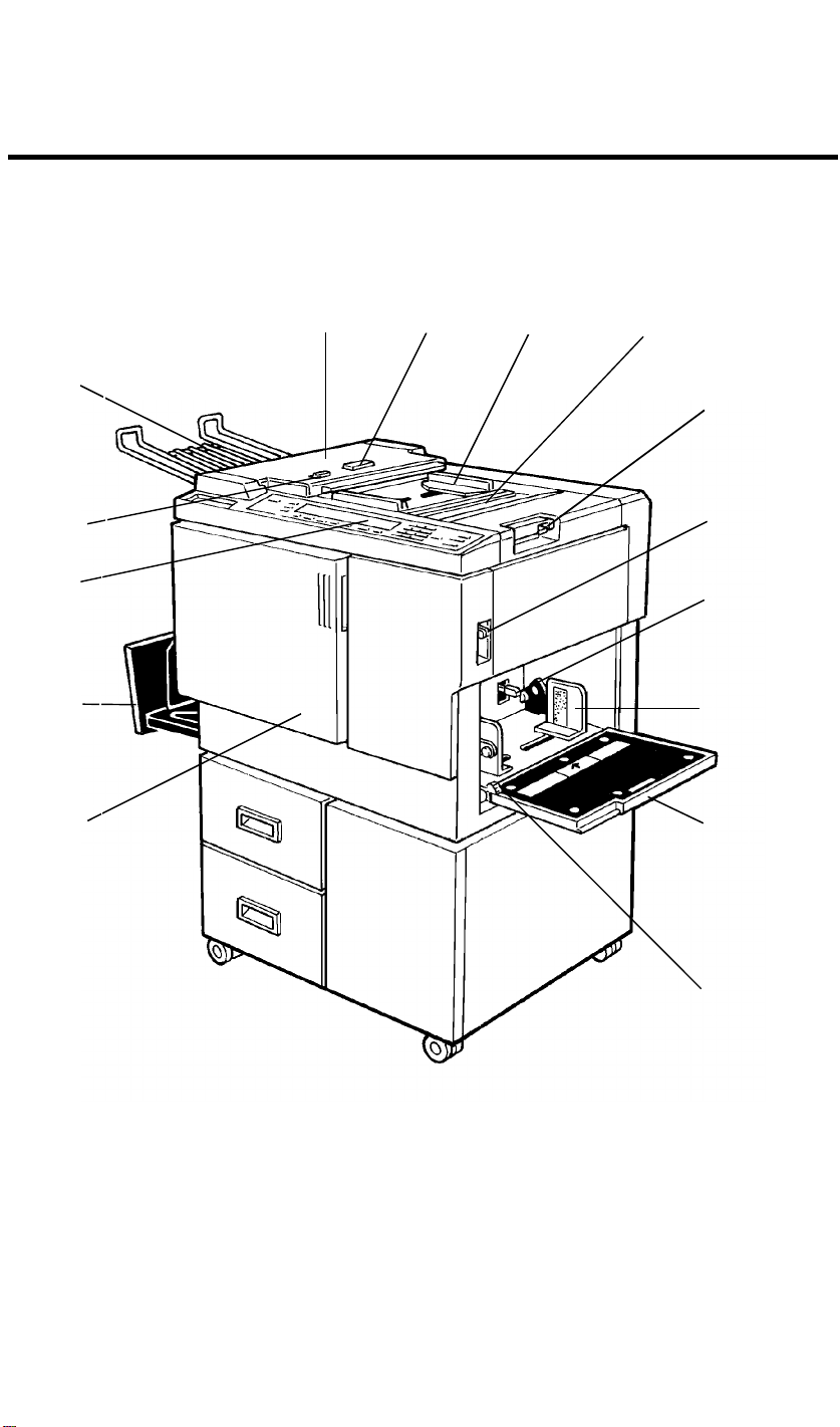
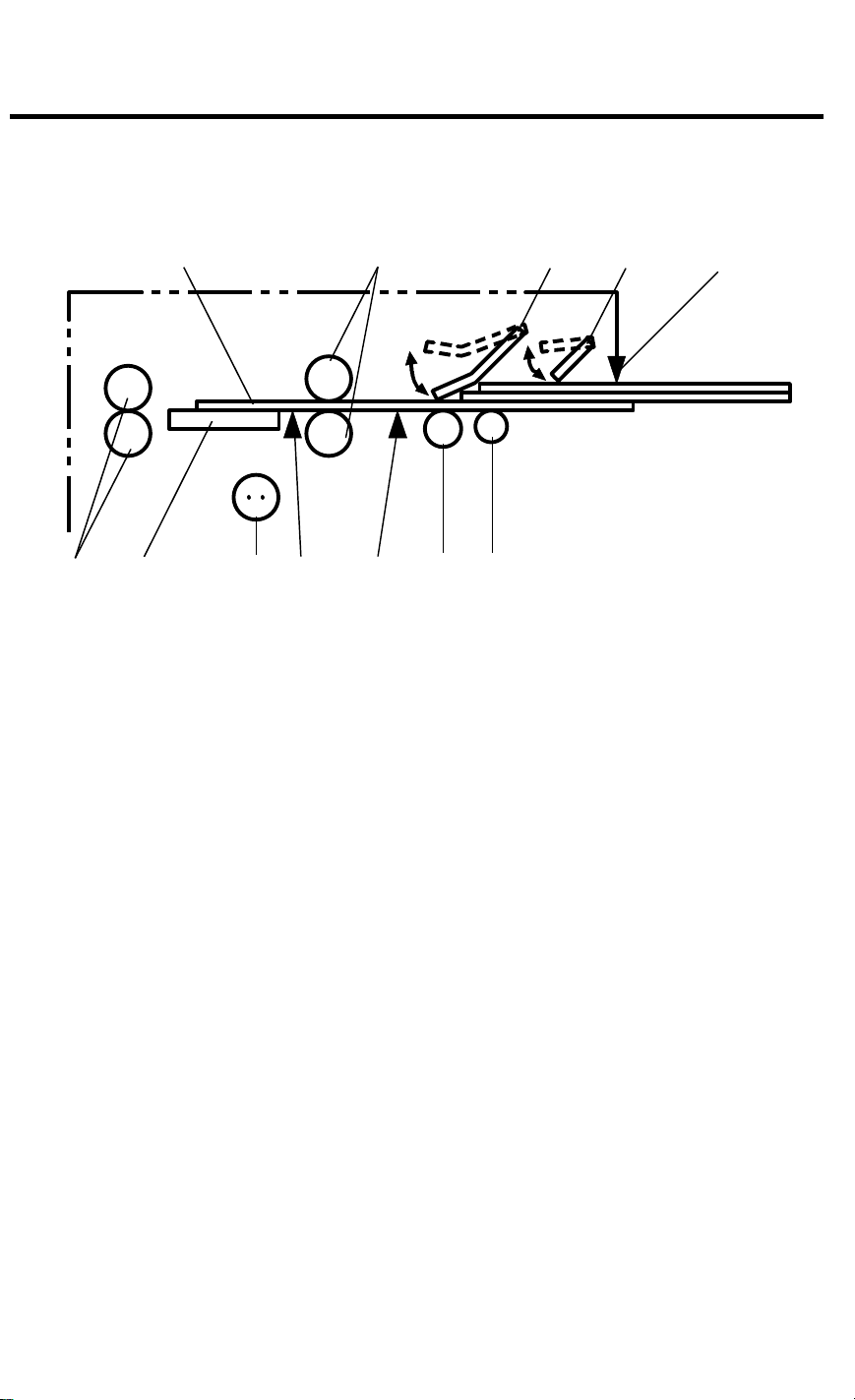
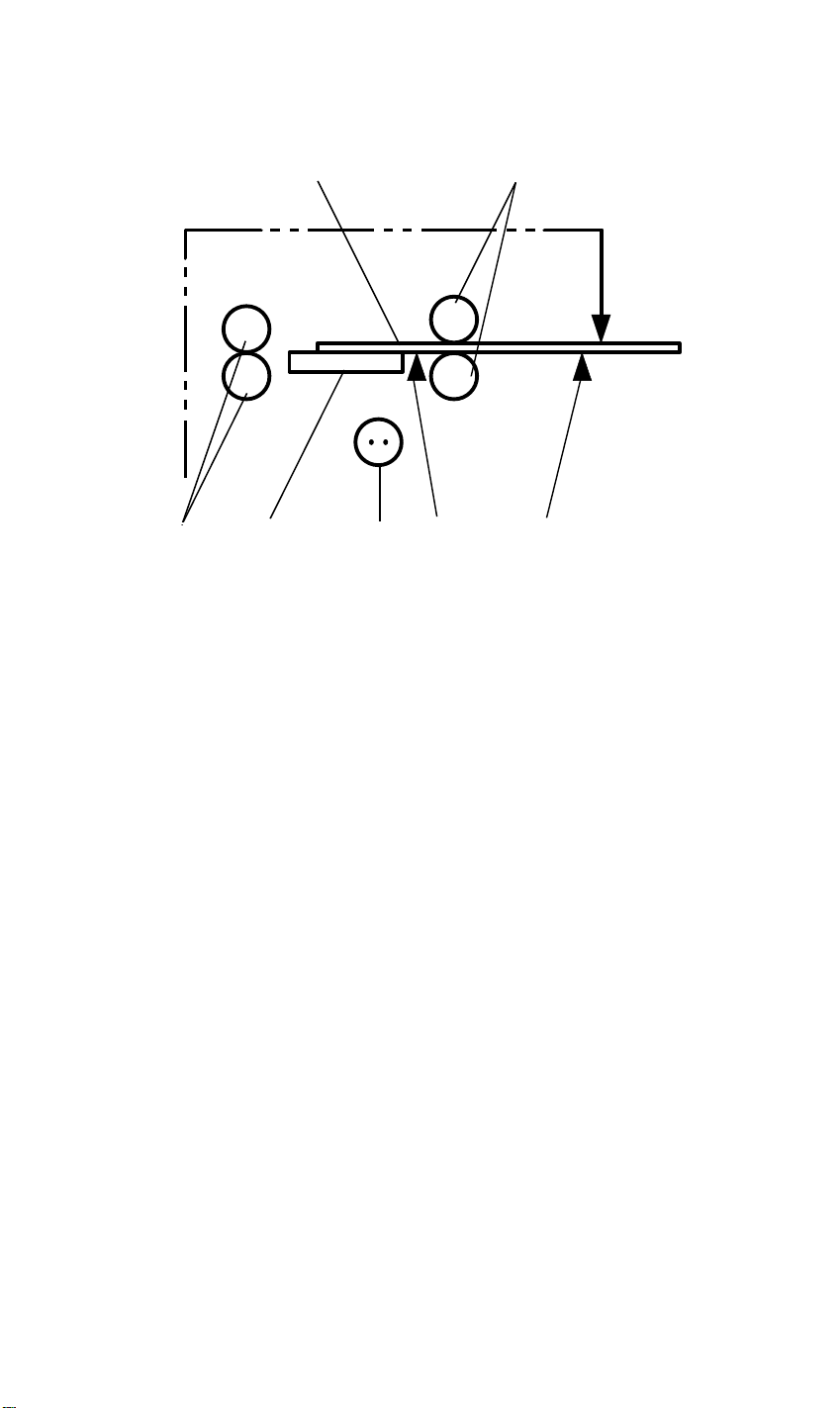
2. GUIDE TO COMPONENTS AND THEIR
FUNCTIONS
(Paper Feed Side)
15
14
13
12
11
1 2 3
4
5
6
7
8
9
1-8
10
Page 11

No. Name Function
28 February ’91
1. ADF Unit
(VT2300/2500)
2. ADF Unit Open
Feeds the original to the printing position
automatically.
Use to open the ADF unit.
Button
(VT2300/2500)
3. Original Guides Adjust these guides to position the originals
correctly.
4. Original Table Place the originals on this table.
5. Original Table
Release Lever
6. Feed Roller
Pressure Lever
7. Separation Roller
Pressure Lever
8. Paper Feed Side
Use to open the original table unit to the left for
master installation.
Use to adjust the contact pressure of the paper
feed roller according to paper thickness.
Use to adjust the separation roller pressure to
prevent double feed.
Use to prevent paper skew.
Plate
9. Paper Feed Table Set the paper on this table.
10. Side Plate Fine
Use to shift the paper feed table sideways.
Adjusting Dial
11. Front Door Open for access to the inside of the machine.
12. Paper Delivery Table Completed prints are delivered here.
13. Operation Panel Operator controls and indicators are located here.
14. ADF On/Off Select
Switch
When setting originals one sheet at a time, set this
switch to the Off position.
(VT2300/2500)
15. Original Tray Originals used to make a master are delivered to
this tray.
1-9
Page 12
28 February ’91
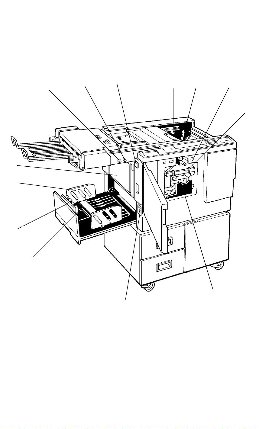
(Paper Delivery Side)
25
24
23
26
27
28
16 17 18
19
22
20
21
1-10
Page 13

28 February ’91
No. Name Function
16. Master Cut Button Press this button to cut the master paper leading
edge after installing a new master roll.
17. Pressure Release
Lever
18. Drum Rotating
Button
Use to install the master roll, or to clean the
thermal head.
Press to replace the drum or to remove misfed
paper.
19. Drum Unit The master paper is wrapped around this unit.
20. Ink Holder Set the ink cartridge in this holder.
21. Main Switch Use to turn the power on or off.
22. Small Size Paper
Delivery End Plate
Use to align the leading edge of small-sized (less
than A4/LT) prints.
(for smaller than
A4/LT)
23. Paper Delivery End
Plate (for larger
Use to align the leading edge of prints larger than
A4/LT.
than A4/LT)
24. Paper Delivery
Use to align the prints on the paper delivery table.
Side Plate
25. Master Eject
Open when removing the master eject container.
Container Cover
26. Memory/Class switch
Use to select memory or class mode.
(VT2300/2500)
27. Skip Paper Feed
Switch (VT2300/2500)
Printing Density
Select Switch
Use to adjust paper feed interval or a misted
master.
Use to select the printing density according to the
type and quality of the original.
(VT2100/2130/2150)
28. Master Eject Unit
Press to remove misfed paper or a misfed master.
Open Button
1-11
Page 14
28 February ’91
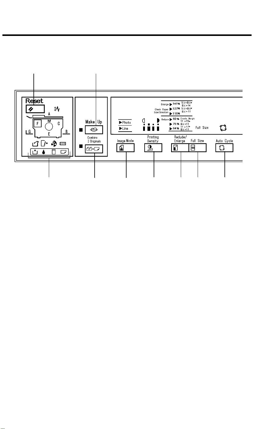
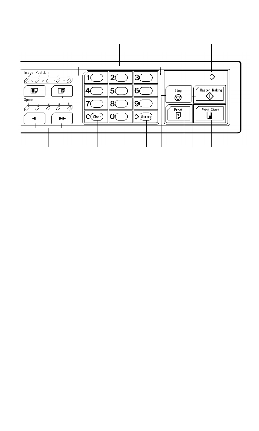
3. OPERATION PANEL
VT2300/VT2500
1
20
1. Reset Key Press to reset error indicators.
2. Make-up Key Press to use the make-up function (VT2500 only).
3. Number Keys Press to enter the number of prints.
4. Stop Key Press to stop the machine operation. The machine
5. Clear Modes Key Press to cancel all previously entered settings and
6. Master Making
Key
7. Print Start Key Press to start printing.
8. Proof Key Press to make trial prints or extra prints.
9. Clear Key Press to change the number set in the counter.
10. Memory/Class Key Use to select group printing in Memory mode or
11. Lower Paper Feed
Table Key
12. Image Position
Keys
2
16
19 18
will continue operation when the Print Start key or
Master Making key is pressed.
modes.
Press to make a master.
Also use to change the make-up mode (VT2500
only). This key can be used only after the machine
stops operation.
Class mode.
Press to lower the paper feed table.
Press to shift the image forwards or backwards on
the print paper.
15
1417
1-12
Page 15
28 February ’91
3
111213
910
4
5
8 7 6
13. Speed Keys Press to adjust the rotation speed of the machine
according to the type of image and printing paper.
14. Auto Cycle Key Use to automatically process masters and make
prints.
15. Full Size Key Press to make prints the same size as the original.
16. Reduce/Enlarge
Press to reduce or enlarge the image.
Key
17. Printing Density
Press to make prints darker or lighter.
Key
18. Image Mode Key Press to select line mode or photo mode according
to the type and quality of the original.
19. Combine 2
Originals Key
Press to combine two originals onto one print
image.
20. Monitors Light or blink when a non-standard condition
occurs within the machine.
1-13
Page 16

28 February ’91
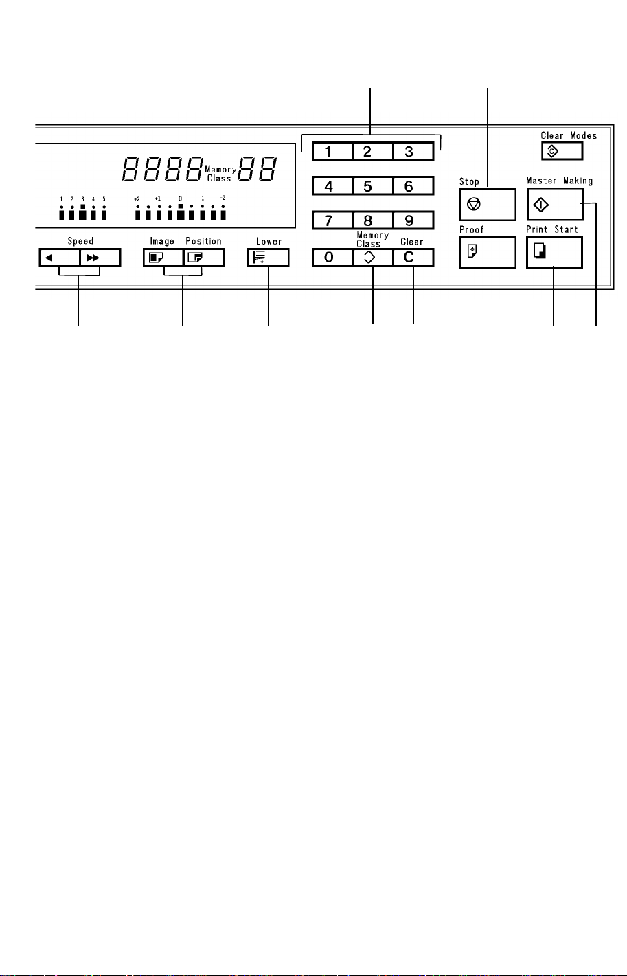
VT2100/VT2130/VT2150
1 2 3 4
18 17
16
1. Reset Key Press to reset error indicators.
2. Indicators Light or blink when a non-standard condition
occurs within the machine.
3. Auto Cycle Key Use to automatically process masters and make
prints.
4. Reduction Key Press to reduce the image.
5. Image Position
Keys
Press to shift the image forwards or backwards on
the print paper.
6. Number Keys Press to enter the number of prints.
7. Counter Displays the number of prints entered. While
printing, it shows the number of uncompleted
prints.
8. Memory Display Displays the number of the memory location that
will be used to store the number of copies. The
print number for up to 10 jobs can be stored at
once.
9. Print Start Key Press to start printing.
10. Master Making
Press to make a master.
Key
11. Proof Key Press to make trial prints or extra prints.
12. Stop Key Press to stop the machine operation. The machine
will continue operation when the Print Start key or
Master Making key is pressed.
1-14
Page 17
28 February ’91
5 6
15
14 13 12
7 8
1110
9
13. Memory Key Use to select memory location number.
14. Clear Key Press to change the number set in the counter.
This key can be used only after the machine stops
operation.
15. Speed Keys Press to adjust the rotation speed of the machine
according to the type of image and printing paper.
16. Image Mode Key Press to select line mode or photo mode according
to the type and quality of the original.
17. Combine 2
Originals Key
18. Lower Paper Feed
Press to combine two originals onto one print
image.
Press to lower the paper feed table.
Table Key
1-15
Page 18
28 February ’91
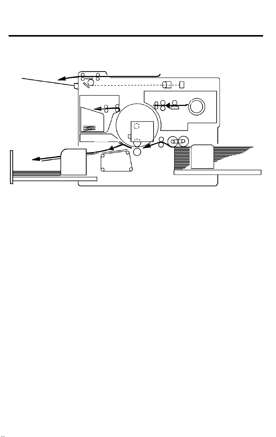
4. PRINTING PROCESS
2
1
6
4
5
1. Master Ejecting: Eject the used master wrapped around the drum
into the master eject box.
2. Scanning: Scan the original image by CCD through the mirror
and the lens while feeding the original.
3. Master Feeding: Convert the image signal read by CCD into the
digital signal and send it to the thermal head to
make holes on the surface of the master and then,
set the master around the drum.
4. Paper Feeding: Send paper to the drum section by using center
separation system consisting of the separation
plate and separation roller.
5. Printing: Press the paper fed from the paper feed section to
the drum to transfer the ink through drum screen
and the master.
6. Paper Delivering: Peel the printed paper with the Exit Pawl and Air
knife and eject the paper onto the paper delivery
table.
3
1-16
Page 19
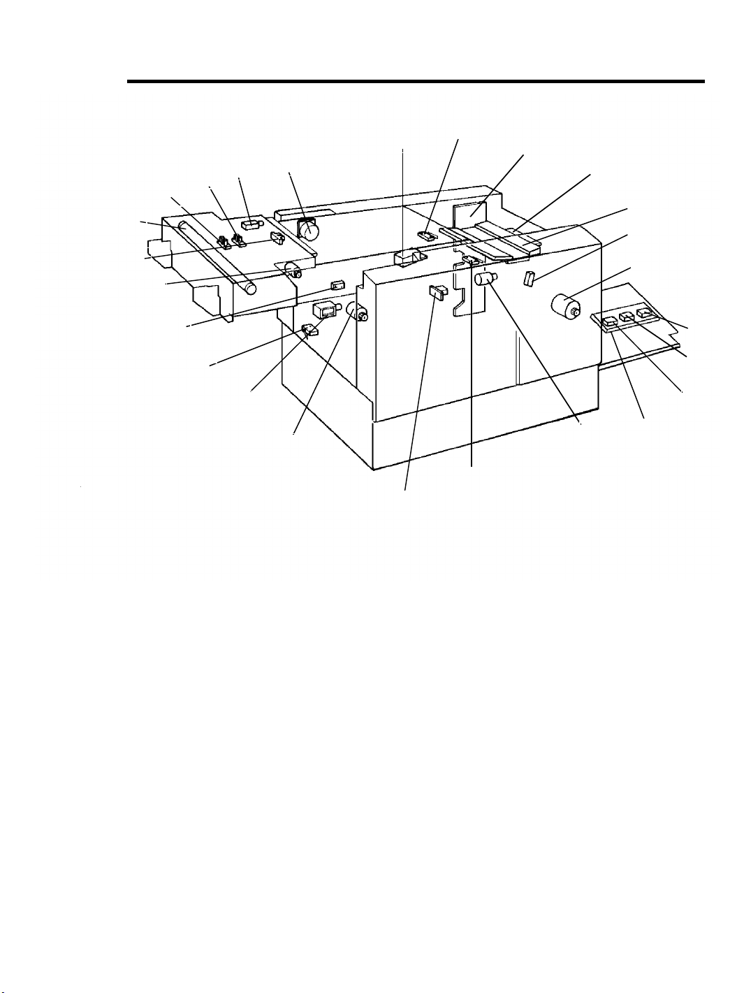
5. ELECTRICAL COMPONENT LAYOUT
28 February ’91
25
24
23
1
22
21
5
3
2
20
4
19
18
6
17
7
8
9
10
11
12
13
14
16
15
1. Original Registration Sensor
2. 2nd Original Sensor
3. Original Pressure Solenoid
(VT2300/VT2500)
4. Original Transport Motor
5. Fluorescent Lamp Stabilizer
6. Right Cutter Switch
7. Power Supply PCB
8. Thermal Head Drive Control PCB
9.Thermal Head
10. Master End Sensor
11. Master Feed Motor
12. Paper Size Detection Sensor 3
(VT2300/VT2500)
13. Paper Size Detection Sensor 2
(VT2300/VT2500)
14. Paper Size Detection Sensor 1
(VT2300/VT2500)
15. Paper Size Detection Board
(VT2300/VT2500)
16. Cutter Motor
17. Left Cutter Switch
18. Master Buckle Sensor
19. Master Eject Motor
20. Master Eject Solenoid
21. Master Box Switch
22. Master Eject Sensor
23. ADF Drive Motor (VT2300/VT2500)
24. 1st Original Sensor
(VT2300/VT2500)
25. Fluorescent Lamp
1-17
Page 20

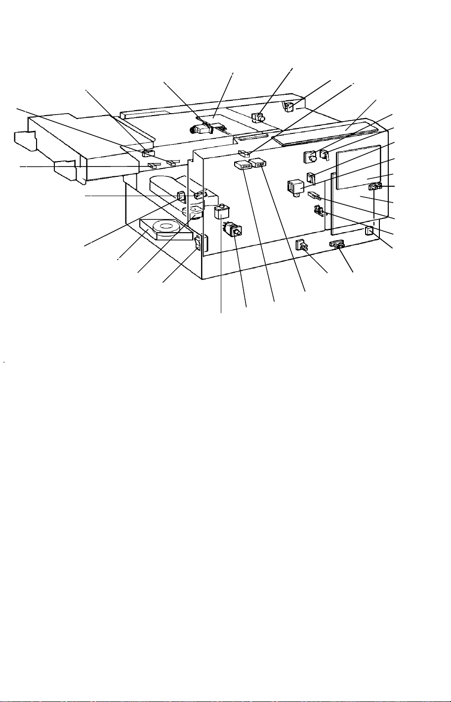
28 February ’91
27
26
28
29
30
31
32
33
34
42
41
35
36
40
37
39
26. Master Eject Clamper Solenoid
27. Ink Detection PCB
28. Master Feed Clamper Solenoid
29. Master Eject Unit Safety Switch
30. Image Shift Motor
31. Reverse Roller Solenoid
32. Encoder
33. 1st Drum Position Sensor
34. 2nd Drum Position Sensor
38
35. Paper Feed Solenoid
36. Paper Table Drive Motor
37. Drum Rotation Sensor
38. Main Motor
39. Printing Pressure Solenoid
40. AC Drive PCB
41. 1st Paper Exit Sensor
42. 2nd Paper Exit Sensor
1-18
Page 21
28 February ’91
71
70
69
68
72
67
66
43
65
64
44
63
62
45
61
46
47
48
49
50
51
52
53
54
55
56
57
58
5960
43. CCD PCB
44. A/D Conversion PCB
45. Master Cutter Switch
46. Scanner Safety Switch
47. Drum Master Detection Sensor
(VT2300/VT2500)
48. Operation Panel
49. Drum Rotation Switch
50. Front Door Safety Switch
51. Drum Safety Switch
52. Ink Supply Solenoid
53. Main Control Board
54. Paper Table Height Sensor
55. Image Processing PCB
56. Drum Lock Solenoid
57. Paper End Sensor
58. Paper Table Safety Switch
59. Paper Table Lower Limit Sensor
60. Printing Pressure Sensor
61. Copy Counter
62. Master Counter
63. Interlock Switch
64. Circuit Breaker
65. Main Switch
66. Air Knife Motor
67. Vacuum Motor
68. Full Master Detecting Switch
69. Pressure Plate Position Switch
70. Memory/Class Switch
(VT2300/VT2500)
71. Skip Paper Feed Switch
(VT2300/VT2500)
Printing Density Switch
(VT2100 /VT2130/VT2150)
72. A.D.F. Safety Switch
(VT2300/VT2500)
1-19
Page 22

28 February ’91
6. ELECTRICAL COMPONENT DESCRIPTIONS
INDEX
No.
Motors
4 Original Transport Motor Transports the original to the scanner
11 Master Feed Motor Feeds the master to the drum. E-3
16 Cutter Motor Cut the master. F-6
19 Master Eject Motor Sends used master into the master
23 ADF Drive Motor Feeds the original to the scanner
30 Image shift Motor Changes the timing between the paper
36 Paper Table Drive Motor Raises and lowers the paper table. F-5
38 Main Motor Drives paper feed, drum, printing and
66 Air Knife Motor Rotates the fan to separate the paper
67 Vacuum Motor Provides suction so paper is held firmly
Solenoids
3 Original Pressure Solenoid Presses the original pressure plate
20 Master Eject Solenoid Moves the master eject roller to contact
26 Master Eject Clamper
Solenoid
28 Master Feed Clamper
Solenoid
31 Reverse Roller Solenoid Releases the clutch to rotate the
35 Paper Feed Solenoid Releases the paper feed sector gear to
39 Printing Pressure Solenoid Moves the press roller against the drum. F-8
52 Ink Supply Solenoid Releases the spring clutch to activate
56 Drum Lock Solenoid Prevents removal of the drum unit
NAME FUNCTION P to P
LOCATION
section.
eject box.
section.
feed roller and the drum to adjust
vertical image position.
paper delivery unit components.
leading edge from the drum.
on the transport belt.
down on the originals.
the drum surface.
Opens the master clamp to eject the
master.
Opens the master clamp to clamp the
master.
reverse roller.
rotate the paper feed roller.
the ink supply pump.
unless the drum is at the original stop
position
(This solenoid can be used on the
VT2300/VT2500).
(VT2300/2500
(VT2300/2500
A-4
F-7
A-4
only)
F-8
F-4
F-7
F-5
A-4
only)
F-6
F-8
F-8
F-6
F-8
F-7
F-7
1-20
Page 23

28 February ’91
INDEX
No.
NAME FUNCTION P to P
LOCATION
Switches
6 Right Cutter Switch Detects when the cutter position is far
right.
17 Left Cutter Switch Detects when the cutter position is far
left.
21 Master Box Switch Checks whether the master eject box is
installed correctly or not.
(VT2300/2500)
(VT2100/2130
29 Master Eject Unit Safety
Switch
Checks whether the Master Eject Unit
is closed correctly or not.
45 Master Cut Switch Informs the CPU to cut the master
paper leading edge.
(VT2300/2500)
(VT2100/2130
46 Scanner Safety Switch Checks whether the scanner unit is
closed correctly or not.
49 Drum Rotation Switch Informs the CPU to rotate the main
motor at 10 rpm.
50 Front Door Safety Switch Checks whether the Front Door is set
correctly or not.
51 Drum Safety Switch Checks whether the drum unit is set
correctly or not.
58 Paper Table Safety Switch Checks whether the paper table is
opened correctly or not.
63 Interlock Switch Releases the cover safety functions. F-4
65 Main Switch Turns the power on or off. B-1
68 Full Master Detecting
Switch
Informs the CPU when the master eject
box is full of masters.
(VT2300/2500)
(VT2100/2130
69 Pressure Plate Position
Switch
Informs the CPU when the pressure
plate has reached the home position.
(VT2300/2500)
(VT2100/2130
70 Memory/Class Switch Selects Memory or Class mode. C-4
(VT2300/2500
F-6
F-6
F-7
F-6
/2150)
F-4
F-8
F-7
/2150)
F-4
A-6
F-4
B-6
F-4
F-7
F-6
/2150)
F-7
F-6
/2150)
only)
1-21
Page 24

28 February ’91
INDEX
No.
71 Skip Paper Feed Switch
(VT2300/VT2500)
Printing Density Switch
(VT2100 series)
72 ADF Safety Switch Check whether the ADF unit is set
Sensors
1 Original Registration
Sensor
2 2nd Original Sensor Detects when the original is set. A-3
10 Master End Sensor Informs the CPU when the plotter unit
12 Paper Size Detection
Sensor 3
13 Paper Size Detection
Sensor 2
NAME FUNCTION P to P
LOCATION
Adjusts paper feed interval to allow
time for user to remove prints.
Use to select the printing density
according to the type and quality of the
original.
correctly or not.
Informs the CPU when the original
leading edge reaches the exposure
glass.
runs out of master roll.
Detects the size of the paper set on the
paper table.
Detects the size of the paper set on the
paper table.
(VT2300/2500)
(VT2100/2130
(VT2300/2500
(VT2300/2500
(VT2300/2500
C-4
C-3
/2150)
B-4
only)
A-3
F-6
E-5
only)
E-5
only)
14 Paper Size Detection
Sensor 1
18 Master Buckle Sensor Detects the master buckle existence. F-6
22 Master Eject Sensor Detects when the used master is sent
24 1st Original Sensor Detects when the original is set in the
33 1st Drum Position Sensor Checks the position of the drum. F-8
34 2nd Drum Position Sensor Checks the position of the drum. F-8
37 Drum Rotation Sensor Supplies timing pulses to the main
41 1st Paper Exit Sensor Misfeed detector. A-5
42 2nd Paper Exit Sensor Misfeed detector. A-5
47 Drum Master Detection
Sensor
54 Paper Table Height
Sensor
Detects the size of the paper set on the
paper table.
into the master eject box.
ADF mode.
board.
Checks whether the master is on the
drum.
Detects when the paper table reaches
the paper feed position.
E-5
(VT2300/2500
only)
F-7
(VT2300/2500)
F-6
(VT2100/2130
/2150)
A-4
(VT2300/2500
only)
F-8
F-6
(VT2300/2500
only)
A-6
1-22
Page 25

28 February ’91
INDEX
No.
57 Paper End Sensor Informs the CPU when the paper table
59 Paper Table Lower Limit
Sensor
69 Printing Pressure Sensor Informs the CPU when the printing
Printed Circuit Board
7 Power Supply PCB Rectifies 100V AC input and supplies
8 Thermal Head Drive
Control PCB
27 Ink Detection PCB Control the ink supply. F-7
40 AC Drive PCB Controls the AC component by relays. E-5
43 CCD PCB Converts the light intensity into the
44 A/D Conversion PCB Converts the analogue signal into the
48 Operation Panel Controls the LED performance and
53 Main Control PCB Controls all machine functions both
55 Image Processing PCB Controls the master processing
Printed Circuit Board
15 Paper Size Detection
Board
Counters
61 Copy Counter Keeps track of the total number of
62 Master Counter Keeps track of the total number of
Others
5 Fluorescent Lamp
Stabilizer
9 Thermal Head Plots the master with heat. F-2
25 Fluorescent Lamp Applies light to the original for exposure. A-3
32 Encoder Converts 16 image positions to 4 bit
64 Circuit Breaker Cuts the ac line off. B-1
NAME FUNCTION P to P
LOCATION
runs out of paper.
Detects when the paper table reaches
the lowest position.
pressure is applied.
DC voltage.
Supplies the power to the Thermal
Head according to the signal from the
scanner section.
electrical signal.
digital signal.
monitors the key operation.
directly and through other boards.
performance.
Detects the size of the paper set on the
table.
copies made.
masters made.
Stabilizes the power supplement to the
Fluorescent Lamp.
data.
(VT2300/2500)
(VT2100/2130
(VT2300/2500
F-5
B-6
/2150)
A-6
A-6
D-1
E-2
A-2
B-3
A-8
C-6
C-3
E-5
only)
A-7
A-7
B-3
F-7
1-23
Page 26

28 February ’91
7. MECHANICAL COMPONENT LAYOUT
17 16 15 1413 109 8 7 6 5 4
18
19
20
21
22
23
24
1. Thermal Head
2. Platen Roller
3. Master Feed Roller
4. CCD
5. Lens
6. Reverse Roller
7. Ink Roller
8. Drum Unit
9. 1st Eject Roller
10. 2nd Eject Roller
1211
333231302928272625
21. Mirror
22. Master Eject Box
23. Exit Pawl
24. Air Knife
25. Delivery Table
26. Delivery Guide Plate
27. Vacuum Unit
28. Press Roller
29. Doctor Roller
30. 2nd Feed Roller
3
2
1
38
37
36
35
34
11. Original Pressure Plate
(2300/2500)
12. Pull-out Roller (2300/2500)
13. Separation Blade (2300/2500)
14. Original Feed Roller (2300/2500)
15. 1st Original Transport Roller
16. Exposure Grass
17. 2nd Original Transport Roller
18. Fluorescent Lamp
19. Original Exit Tray
20. Feed Sub Mirror
31. Lower Separation Roller
32. Separation Plate
33. Paper Feed Side Plate
34. Paper Feed Table
35. Paper Feed Roller
36. Upper Separation Roller
37. Ink Holder
38. Master Spool
1-24
Page 27

SECTION 2
SECTIONAL DESCRIPTION
Page 28
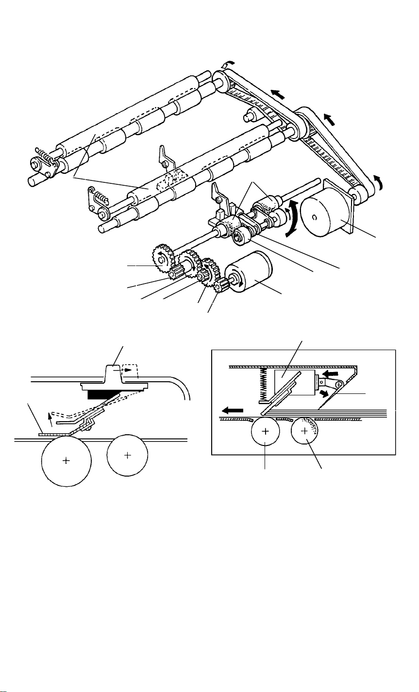
1. ORIGINAL FEED SECTION
1.1 OVERALL: VT2300/VT2500
[I] [G] [E] [B] [A]
28 February ’91
[J] [K] [L] [D] [C]
[J]: 2nd Original Transport Rollers
[K]: Exposure Glass
[L]: Fluorescent Lamp
There are two original feed modes in this model.
ADF Mode: The originals [I] set on the original table are detected by the
1st original sensor [A]. When the Master Making key is
pressed, the original pressure plate [B] presses the originals
down. The pull-out roller [C] starts moving the lowest original
forward at the same time. The lowest original is separated
from the other originals by the original feed roller [D] and the
separation blade [E]. When the 2nd original sensor [F] detects the original, the 1st original transport rollers [G] start
rotating. The rollers stop after the original activates the original registration sensor [H]. The 1st original transport rollers
start rotating again after the drum section completes the
preparation for the master making.
[F][H]
SADF Mode: The separation blade [E] is released in the SADF mode. The
original on the original table is fed to the starting position
when the 2nd original sensor [F] detects the original.
2-1
Page 29
28 February ’91
1.2 OVERALL: VT2100/VT2130/VT2150
[I] [G]
[J] [K] [L] [H] [F]
[J]: 2nd Original Transport Rollers
[K]: Exposure Glass
[L]: Fluorescent Lamp
[H]: Original Registration Sensor
The original [I] set on the original table is detected by the 2nd original
sensor [F]. At the same time, the 1st original transport rollers [G] and 2nd
original transport rollers [J] start rotating and feed the original to the original
start position where is 12 mm far from the guide plate. The original
transport rollers start rotating again after the drum section completes the
preparation for the master making.
2-2
Page 30
28 February ’91
1.3 ORIGINAL FEED DRIVE MECHANISM: VT2300/VT2500
[J]
[A]
[B]
(f)
(e)
[C]
(c)(d)
(b)
[D]
[E]
(a)
[I]
[H]
[G]
[F]
[J] [D]
The original transport rollers [A] are driven by the original transport motor
[B], which is a stepper motor. The original feed rollers [J] are driven by the
ADF drive motor [C] through a series of gears [(a) to (f)]. The ADF drive
motor is a dc motor. The pull-out rollers [D] are driven by the ADF motor
through a drive belt [E].
The original pressure plate [F] is pressed down on the originals by the
original pressure solenoid [G]. The separation blade [H] is moved up and
down by the ADF ON/OFF select switch [I].
2-3
Page 31

28 February ’91
1.4 ORIGINAL FEED DRIVE MECHANISM: VT2100/VT2130
/VT2150
[G]
[F]
[I]
[H]
[A]
[B]
[E]
[D]
[C]
When the actuator [A] is pressed down by the original, the 2nd original
sensor [B] is activated and the original transport motor [C] starts rotating.
The rotation of the original transport motor is transmitted to belts [D] and [E]
to turn the lower first original transport roller and lower second original
transport roller. At the same time, both the upper original transport rollers
[F] contact the first and second lower original transport rollers due to
pressure from the springs [G]. The rollers rotate and the original is fed.
When the actuator [H] is pressed down by the original, the original
registration sensor [I] is activated and the original transport motor stops.
When the Master Making key is pressed, the original transport motor rotates
to read the original after the master eject process is finished.
The distance between the sensors is 50 millimeters. If the original
registration sensor is not activated within five seconds, "A" and
indications blink.
2-4
Page 32

1.5 ELECTRICAL TIMING: VT2300/VT2500
(One Original):
Insert Original
2nd Drum Position Sensor
Master Making Key
1st Original Sensor
Fluorescent Lamp
ADF Drive Motor
Original Pressure Solenoid
2nd Original Sensor
Original Registration Sensor
Original Transport Motor
Master Feed Motor
Read Command
T1
T2
T3
425 ms
T7
T4
Drum
Rotates
120°
T5
Original Feeds 25 mm
T6
Original
Feeds 14 mm
Master Feeds 438 mm
28 February ’91
T4:
Exposure Glass
Original Stop Position
12 mm
Scanning Position
16 mm
Original
Guide Plate
T1: When originals are inserted in the ADF unit, the 1st original sensor is
activated.
T2: When the Master Making key is pressed, the ADF drive motor starts
rotating and the pull-out roller and original feed roller feed the 1st
original. At the same time, the original pressure solenoid is energized
and the pressure plate presses the originals against the pull-out
rollers.
T3: When the 2nd original sensor detects the original, which is separated
by the separation blade and the original feed roller, the original
transport motor starts rotating and the transport rollers start rotating.
T4: One original is fed and when the original registration sensor detects
the original, the original transport motor stops the original position is
then as shown above.
T5: After the master eject process is finished and the second drum
position sensor is activated, the drum rotates 120 degrees more and
then the original transport motor turns on.
2-5
Page 33

28 February ’91
T6: After the original is fed 14 millimeters, master feeding and master
making start.
T7: The ADF drive motor and the original pressure solenoid are turned off
425 mseconds after the 2nd original sensor detects the original.
If 2nd original sensor is not activated within 2.3 seconds after
pressing the Master Making key, the Original Misfeed indicator (A +
) will start blinking.
2-6
Page 34

(Make-up mode): VT2500 only
Insert
Command
Sheet
Command Sheet Transportation
28 February ’91
Original
Transportation
Master Making Key
1st Original Sensor
Fluorescent Lamp
ADF Drive Motor
Original Pressure Solenoid
2nd Original Sensor
Original Registration Sensor
Original Transport Motor
Read Command
(Command Sheet)
Read Command (Original)
Make-up Key
T4:
T1
T0
T2
T3
41.6 msec
2 mm
Scanning Position
T4
16 mm
425 msec
Original Feeds
25 mm
Original Feeds
2 mm
Command Sheet
Guide Plate
Master Ejecting Start
425 msec
T5
T0: When the Make-up key is pressed, the fluorescent lamp turns on.
T1: When the original is inserted with a command sheet, the 1st original
sensor is activated.
T2: When the Master Making key is pressed, the ADF drive motor turns
on and the command sheet is fed by the pull-out rollers and the
original transport rollers. At the same time, the original pressure
solenoid is energized and the original pressure plate presses down
on the original and the command sheets.
T3: The original transport motor starts rotating when the 2nd original
sensor is activated by the command sheet.
T4: The reading command is output when the command sheet is fed
2mm past the scanning position.
T5: The original transport motor stops rotating when the command sheet
is fed 25 mm past the original registration sensor. At the same time,
the reading command turns off. The ADF drive motor and the original
pressure solenoid turn on at the same time and the original is fed.
2-7
Page 35

28 February ’91
1.6 ELECTRICAL TIMING: VT2100/VT2130/VT2150
Original Set Master Making Key "ON"
2nd Drum Position Sensor
2nd Original Sensor
Original Registration Sensor
Original Transport
Fluorescent Lamp
T1
T2
Drum Rotation Degree
o
120
T3
T5
Reading Command
Master Feed Motor
T2:
No Image Area:
10 mm
Scanning Position
NOTE: The original stops 12 millimeters
16 mm
away from the corner of the
12 mm14 mm
lower guide plate edge [A].
Original Feed
Length (14 mm)
[A]
T4
Master Feed Length
(438 mm VT2100/VT2130)
(371 mm VT2150)
T1: When the 2nd original sensor detects the original, the original
transport motor starts rotating.
T2: One original is fed and when the original registration sensor detects
the original, the original transport motor stops the original position is
then as shown above.
T3: After the master eject process is finished and the second drum
position sensor is activated, the drum rotates 120 degrees more and
then the original transport motor turns on.
T4: After the original is fed 14 millimeters, master feeding and master
making start.
T5: The master feed motor stays on until it feeds the master 437 mm.
The original transport motor stops when the master feeding stops. At
that time the fluorescent lamp also turns off.
2-8
Page 36

28 February ’91
1.7 CIRCUIT:
Original
Registration
Sensor
2nd Original
Sensor
Original
Transport Motor
M
Image
A/D
Conversion P.C.B.
1
3
2
1
3
2
5V
CN603-1
CN603-4
CN603-2
GND
CN603-3
CN601-13
CN601-11
CN601-25
(CN601-27)
CN601-17
CN601-18
CN601-19
CN601-20
CN601-21
Processing
P.C.B.
CN403-13
CN403-11
CN403-25
(CN403-27)
CN403-17
CN403-18
CN403-19
CN403-20
CN403-21
Fluorescent Lamp
VT2300/VT2500 only:
1st Original
Sensor
ADF
Drive Motor
Original Pressure
Solenoid
ADF Safety SW
M
SOL
Stabilizer
CN611-1
CN611-2
CN612-1
CN612-2
1
3
2
CN604
Red
-1
CN604
Yellow
-3
CN604-2
Black
CN607-3+5V
CN607-5 CN601-3
CN607-4 (GND)
CN607-6
CN607-7
CN607-1
CN607-2
CN607-8
CN607-9
24V
+24V
CN601
-15
GND
+5V
CN601-5
+24V
CN601-1
CN601-7
CN601-9
CN403-15
CN403-3
CN403-5
CN403-1
CN403-7 (IN)
CN403-9 (OUT)
2-9
Page 37

28 February ’91
1.8 OUTPUTS:
Signal Name I/O
A/D Conversion Board
CN No. Level
Fluorescent
Lamp O CN601-15
Reading
Command I
CN601-25
(CN601-27)
ADF Drive
Motor
(VT2300/VT2500)
I (CN607-6)
Original
Pressure SOL
(VT2300/VT2500)
O (CN607-2)
Original
Registration
O CN603-4
Sensor
2nd Original
Sensor I CN603-3
1st Original
Sensor
(VT2300/VT2500)
I (CN607-5)
0V
3V
24V
24V
7.5V
7.5V
0V
3V
0V
0V
0V
5 m
5 m
5V
Description
When the fluorescent lamp turns
on, the voltage of the CN601-15
is 3V.
When the CCD reads the original
the voltage of CN601-25
(CN601-27) is 0V.
When the ADF drive motor starts
rotating, the voltage of CN607-6
is 0V.
When the original pressure
solenoid is energized, the voltage
of CN607-2 is 0V.
When the original registration
sec
sensor is activated, the voltage of
0V
CN603-4 is 0V.
When the 2nd original sensor is
sec
activated, the voltage of CN603-3
0V
is 0V.
When the 1st original sensor is
activated the voltage of CN607-5
is 5V.
( ): VT2300/VT2500
2-10
Page 38

2. OPTICS/IMAGE PROCESSING
2.1 OVERALL
28 February ’91
[D]
Thermal Head
[E]
[F]
[C]
Thermal Head
Control
Operation Panel
[A]
A/D Converter
Image Processing
Main Board
[B]
[C]: Shading Plate
[D]: Mirror
[E]: Exposure Glass
[F]: Fluorescent Lamp
The light reflected from the original goes through the lens [A] and is
changed to an electrical signal in the CCD [B].
The electrical signal from the CCD is converted from an analog signal to a
digital signal in the A/D converter.
The converted digital image data is modulated and edited (VT2500) and is
sent to the thermal head control PCB.
2-11
Page 39

28 February ’91
2.2 LIGHT SOURCE
[B]
[D] [G]
[B]
[A][K]
[D] [C]
[F]
[A]
[E]
[H]
[I]
[J]
[G]: Exposure Glass
[H]: Lens
[I]: CCD
[J]: A/D Converter
[K]: Mirror
The high frequency fluorescent lamp [A] is used as a light source for the
high speed reading of 16 pixels/mm. The light exposes at two angles using
a sub mirror [B] to prevent the shades at the edges of paste-ups on the
original [C]. The original guide plate [F] blocks part of the direct light from
the fluorescent lamp to make the light intensity of both direct and reflected
light the same. A heater [E] is wrapped around the fluorescent lamp. It
prevents light intensity reduction due to low temperature.
<Fluorescent Lamp>
Form: 15.5 ∅ x 436 mm
Lamp Voltage : 59 ± 6 V
---- Platen Cover ----
The platen cover [D] is used as a standard white level reference to correct
for shading distortion.
2-12
Page 40

2.3 LENS
28 February ’91
Original
Surface
312.5∅
5 mm
404.179 mm
Exposure Glass
30.655 mm
[A]
29.895 mm
35∅ mm
[B]
[C]
This consists of 6 lenses, to transfer the image, correctly oriented, to the
photoelectric elements of the CCD. It is possible to adjust the focus by
moving the lens assembly [A].
<Lens>
Focal distance: 43 mm (43.05 ± 0.32 mm)
F No.: F4.5
The above illustration shows the layout to transfer the image from an A3
original (297 millimeter width) to the CCD [B].
<CCD>
Number of effective pixels: 5000 pixels
Reading length: 312.5 mm
Photo signal storage time: 3 msec.
The shading plate [C] corrects light intensity distortion. The light intensity is
low at the both ends of the lamp and is also low at the edge of the lens.
Therefore, the center light is cut to make the light intensity uniform.
2-13
Page 41

28 February ’91
2.4 CCD (Charge Coupled Device)
Shift Registor
Shift Gate
D
31
Shift Gate
Shift Registor
10
φ1E
13 14
S1 S2
D35D34D33D
32
9
1 8
SSφ10φ2Bφ2CRS
15
SSSSφ20
RS2
OS2
OS
RS1
OS1
OD φ2E
18
20
2
5
3
19 17 21
22
φ1Bφ1C
D18D19D
20
6
4
CCD (16 dots/mm) φ1E, φ2E Clock (Phase 1)
φ10, φ20 Clock (Phase 2)
Light
Energy
Shift
Electrode
01B : Final Clock (Phase 1)
02B : Final Clock (Phase 2)
SH : Shift Gate
Photo
Diode
Shift Register
Storage
Electrde
RS : Reset Gate
OS : Output Transistor source
OD : Output Transistor Drain
SS : Sub-straight (Ground)
IS : Input Source (Test Pin)
IG : Input Gate (Test Pin)
7
IS
12
SH
16
IG
This is a solid-state device similar to a photodiode array, but unlike a photodiode array, a CCD can read one complete scan line at a time. The CCD
produces an analog signal which is converted into a digital signal for image
processing.
2-14
Page 42

28 February ’91
2.4.1 Function
The principle circuit of each pixel in the CCD is shown above. The light
reflected from the original is absorbed in the photodiode and the capacitor
stores the charge corresponding to the light intensity.
The CCD is composed of many such pixel elements in series. The image
signal of each pixel element is stored in the shift register as a charge.
When the SH signal is input, the image signal stored in the shift register, is
output in serial as the OS signal.
SH : Shift Gate
The storage electrode charge in the exposure section is transmitted to the
shift register by the shift gate pulse.
φ1E, φ2E Clock (Phase 1)
This is the transmission clock for analog shift register 2 (even pixels).
φ10, φ20 Clock (Phase 2)
This is the transmission clock for analog shift register 1 (odd pixels).
The shift gate signal transmits the electrical charge in parallel to either
analog shift register 1 or 2 (odd or even pixels). At the same time, the photo
signal storage of the next scan line starts in the exposure section.
The transmission clocks serially shift the electric charge transmitted to the
shift register, which outputs it from the OS (output signal) terminal.
2-15
Page 43

28 February ’91
2.4.2 The Image Signal :
CCD Board
+12V
GND
CN801-2
RS
CN801-4
OS
CN801-6
1B
CN801-8
2B
CN801-12
20
CN801-14
10
CN801-16
2E
CN801-18
1E
CN801-20
SH
CN801-9, 10
CN801-1, 3, 5, 7, 11, 13, 15, 17, 19
CN602-1, 3, 5, 7, 11, 13, 15, 17, 19
CN602-2
CN602-4
CN602-6
CN602-8
CN602-12
CN602-14
CN602-16
CN602-18
CN602-20
CN602-9, 10
A/D Converter
A/D Converter
Input
Output
∅10, ∅1B, ∅1E (CN801-14, 6, 18)
∅20, ∅2B, ∅2E (CN801-12, 8, 16)
LSYNC (5,120)
{
SH
∅10, ∅1B, ∅1E
∅20, ∅2B, ∅2E
RS
OS
{
SH (CN801-20)
RS (CN801-2)
OS (CN801-4)
3 ms (5,120 Count)
4,096
Photo Signal Storage Time (3 ms)
Dummy
Pixels 32
Effective
Pixels
5,000
Dummy Pixels 4
Empty Data 84
5,120
Dummy Pixels:The dummy pixels generated by the area covered with alumi-
num film. The dummy pixels are used as the standard black
level.
The first 32 pixels read (D0 to D31) are dummy pixels. Pixels D32 to
D5,032 are the effective pixels (S1 to S5,000). After that there are four
more dummy pixels. Therefore, the total pixel count from the CCD, including
the dummy pixels, is 5,036.
As the image signal captured by the CCD is clocked out by the shift gate
every 3 ms (scan line period), there remains time for 84 transmission clock
pulses after all the image data from the CCD has been output. These clock
pulses, after all valid data have been clocked out, constitute empty data.
During this period, subscanning occurs.
2-16
Page 44

2.5 A/D CONVERSION BOARD
Outline: VT2100/VT2130/VT2150 Circuit
Original
28 February ’91
VPH
Peak
Hold
PKHTM
CCD
Board
Selector 1
80%
53%
6%
PHOTO SHMRT
OS
Selector 2
0
1
2
3
0
1
2
3
A B
Signal Conversion
Direct Current Clamp
Amplification
Counter
CK
LUF
4-bit A/D
Conversion
VH VL
Current
Voltage
Conversion
4 bit
Black Level
Correction
Image
Processing
P.C.B
4 bit
Shading
Distortion
Memory
8-bit D/A
Conversion
VR(+) VR (-)
Selector 2
0: Shading Distortion Correction in Photo mode
1: Shading Distortion Correction in Line mode
2: Line mode
3: Photo mode
The CCD reads the light of the fluorescent lamp reflected from the original.
The CCD and A/D conversion boards convert the analog signals into digital
signals which are transmitted to the image processing board.
2-17
Page 45

28 February ’91
2.5.1 CCD Output Signal Conversion, DC Clamping, Amplification:
VT2100/VT2130/VT2150 Circuit:
+12V
602-4
DCREST
OS
a
SH
Approx. 6V
OS
-12V
+12V
Q607
C669
DC Clamp
Switch
6V
IC628
4.7K
2.2K
IC624
2
_
6
3
+
b
1.7V 1.7V
(VT2300/VT2500:
VR600
R2
IC620
+
_
+5V
TP600
V0
c
IC624-6
Approx. 1.7V
(VT2300/VT2500: 1.4V)
SH
1.7V
(VT2300/VT2500: 1.4V)
DCREST
14 pixels
1). Signal Conversion
The CCD output (OS) varies according to the reflected light intensity and is
clipped at 6 volts. The output signal is then buffered, inverted and amplified.
2-18
Page 46

28 February ’91
2). DC Clamping
The OS signal is amplified by Q607. The dc clamping switch is turned
ON/OFF by the DCREST signal. The switch turns on when the CCD
produces black level (empty data) at the end of scanning and is off during
image scanning.
When the switch turns on, the black level signal is stored in capacitor C669.
When the switch turns off, the black level signal is input to IC624 pin 3
while the image signal is input to the IC624 pin 2.
The difference between the image signal and the black level signal is
amplified and output from the IC624.
This output signal from IC624 is amplified again in IC620. The signal then
goes in the A/D converter.
2-19
Page 47

28 February ’91
2.5.2 Peak Hold:
CCD Board A/D Conversion Board
CCD
Image
Processing
Board
Read
Write
S LSYNC
S CLK
OS
(CN403-27)
CN403-25
(CN403-29)
CN403-27
(CN403-31)
CN403-29
(CN403-33)
CN403-31
Inverter Amp
Timing
Signal
Generator
( ): VT2300/VT2500
Vo
PKHTM
PKHST
BLSET
SHMRT
A/D Conversion
SW2
Peak Hold
Circuit
A/D Conversion
VPH
This circuit holds, at different stages of image processing, the peak white
levels for both the original and the platen cover (standard white). The peak
white, or maximum, level is stored as charge on a capacitor. The peak hold
circuit is cleared by discharging the capacitor.
1). Platen Cover Peak Hold (Standard White)
The platen cover peak hold is used as standard white when processing
data to create the shading distortion data, which is later stored in memory.
This data is used to correct such distortions as bright or dull spots on the
lamp or variations in the CCD output. To create the platen cover peak hold
(standard white), the peak hold circuit stores the maximum level from five
scan lines of the platen cover.
2). Original Background Peak Hold
The maximum white level of the original, stored in the peak hold circuit, is
used to shift the threshold voltage of the D/A converter to match the original
background. An area of the original, 64 mm wide (from S2,048 to S3,072),
is read. This corresponds to a small size original.
3). Peak Hold Set Signal
The peak hold set signal (PKHST) clears the peak hold circuit. The peak
hold timing signal (PKHTM) turns on the analog switch (SW2) allowing the
image signal to be applied to the peak hold circuit.
2-20
Page 48

4) Peak Hold Signal Timing:
L. SYNC
CN403-29
(CN403-31)
Reading
CN403-25
(CN403-27)
Write Out
CN403-27
(CN403-29)
SHMRT
PKHST
PKHTM
5 lines
5 lines
A
BLSET
SW2
Correction Timing
P.H. Signal Input
Timing
ON OFF ON OFF
( ): VT2300/VT2500
A Section (Main Scanning)
LSYNC
PKHTM
0
Original Background
Peak Hold
2080 3140 4096 5120
1024
Image
Reading
Pixels (64 mm width in the middle)
Page 49

28 February ’91
2.5.3 Shading Distortion Correction:
Amp
Pixels Data
PKHTM SW2
Peak
Hold
Circuit
L. SYNC CN403-29
(CN403-31)
Read CN403-25
(CN403-27)
Write CN403-27
(CN403-29)
SHMRT
VPH
53%
B
1 X
Y1
Current/
Voltage
Convertor
VT2100/2130/2150: 1.7V
VT2300/VT2500: 1.4V
5 lines
VH
A/D
Converter
VL
D/A
Converter
VR(+)
4 bit Signal
Shading
Distortion
Memory
4 bit Signal
VR(-)
1.7V: VT2100/2130/2150
1.4V: VT2300/VT2500
SHMRT
PKHST
PKHTM
BLSET
( ): VT2300/VT2500
Shading Distortion Memory
Since the output of the CCD varies according to both the CCD and the
intensity of the fluorescent lamp, shading distortion is corrected electrically
as well as mechanically (shading plate).
2-22
Page 50

1). Shading Distortion Memory
White Peak Hold of Platen Cover
VPH
28 February ’91
VT2100/2130/2150: 1.7V
VT2300/2500: 1.4V
Memory
100%
53%
5,000 pixels
4 bits
When reading the white level of the platen cover, the peak hold (standard
white) is determined using the five scan lines.
The shading distortion data is stored in memory during the fifth scan line .
The potential difference between the output of each pixel and the 53% level
of the peak hold is converted by an A/D converter into 4-bit data. This data
is stored in a memory location corresponding to the pixel.
2). Shading Distortion Correction
White Peak Hold of Original Background
VPH
Correction Memory
100%
53%
VT2100/2130/2150: 1.7V
VT2300/2500: 1.4V
4 bits for
distortion memory
Fixed 4 bits
When reading the original, the distortion data corresponding (stored in
memory) to each pixel is converted from digital to analog, using the D/A
converter, and used as the reference voltage (VH) of the A/D converter.
The D/A converter is an 8-bit converter with 4 of its 8 bits fixed. This
ensures that the output of the D/A converter is always greater than 53% of
the reference voltage (VR+).
2-23
Page 51

28 February ’91
The reference (VR+) of the D/A converter is set to the peak hold of the
original background. Distortion correction is obtained by using the output
voltage of the D/A converter as the reference voltage (VH) of the A/D
converter; therefore, distortion correction also corrects for the original
background level.
For Example: If the light intensity at a certain pixel is very high, then a high
voltage level will be stored in the distortion memory location for that pixel.
When reading a document, that high voltage level is used as the reference
level (VH) of the A/D converter. Therefore, during conversion, the input level
from the pixel is compared to a high voltage by the A/D. This negates any
errors caused by the high light intensity at that pixel.
2-24
Page 52

2.5.4 Original Background Correction
VT2100/2130/2150: 1.7V
VT2300/2500: 1.4V
White Peak Hold of Platen Cover
VPH
28 February ’91
<Original background is lighter.>
Peak Hold of Original Background
VPH
53%
53%
<Original background is darker.>
Peak Hold of Original Background
VT2100/2130/2150: 1.7V
VT2300/2500: 1.4V
VPH
53%
VT2100/2130/2150: 1.7V
VT2300/2500: 1.4V
As the white peak hold of the original background is used as the reference
(VR+) of the D/A converter, the overall shading distortion correction level is
adjusted for the original background at the output of the D/A converter.
For Example, if the background level of the original is low, the reference
level (VH) of the D/A converter is low, causing the overall distortion
correction level to be low. Therefore, even though the light level from the
original background is low, it is being compared to a low reference level
(VH) which causes it to be detected as background, not image.
2-25
Page 53

28 February ’91
2.5.5 Black Level Correction (Line mode only)
Selector 1 0
1
2
3
4
5
6
Counter
CK
Amp.
VT2100/2130/2150: 1.7V
VT2300/2500: 1.4V
Selector 2
Y3
VS
4-bit A/D Conversion
LUF
VL
The black level correction compensates for the image density. Black level
correction is used only when in line mode.
The lower threshold level (VL) of the A/D converter is set according to a
high density original or a low density original.
At first, the black level reference of the A/D converter is set to 35% of the
original peak hold white level (PH) because the analog switch of selector-1
is set to the "0" position.
If while reading the original image the black level of the image is lower than
VL (PH x 35%), the A/D converter outputs the LUF signal.
The LUF signal is applied to selector 1 as a clock pulse. The LUF signal
increments the counter of selector 1 from 0 to 1. This changes the VL to
30% of PH. If the LUF signal is again applied to the counter of selector 1,
incrementing it from 1 to 2, the analog switch of selector 1 changes from 0
to 1.
The following table shows the number of clock pulses needed to increment
the analog switch of selector 1.
Counter (4 bit) Selector 1 Switching VL
0.1 SW 0 PH x 35 %
2.3 SW 1 PH x 30 %
4.5 SW 2 PH x 25 %
6.7 SW 3 PH x 20 %
8.9 SW 4 PH x 15 %
A.B SW 5 PH x 10 %
C.D SW 6 PH x 5 %
E.F SW 7 PH x 0 % (Black Level)
2-26
Page 54

2.5.6 A/D Conversion
28 February ’91
VH
(White Standard)
OS
4 bit A/D
Convertion
VT
(Black Standard)
65%
35%
VT2100/VT2130/VT2150 Circuit:
Amp
VPH of Platten/
Original
Background
VPH of Shading
Distortion
Memory
Black Level
Correction
Output of
Selector 1
SW
VPH x 80%
VPH x 53%
VPH x 6%
PHOTO
Back Ground (White Peak)
A B
Selector 2
0
1
2
X
3
0
1
Y
2
3
A B
A B
0
BAD1
1
2
3
BAD2
4
5
6
BAD3
7
8
9
BAD4
10
11
12
13
14
15
BAD1
BAD2
BAD3
BAD4
1
0
1
0
0
0
1
0
VS
VH
M1
M2
VL
A/D CONVERSION
SHMRT
PHOTO SHMRT
Selector 2 (X,
Y)
Shading Distortion Correction (Photo Mode) L L SW0 ON
Shading Distortion Correction (Line Mode) H L SW1 ON
Photo Mode L H SW2 ON
Line Mode H H SW3 ON
This circuit converts the analog input signal (VS) to a 4-bit digital signal
using both the white level reference (VH) and the black level reference (VL).
In each mode, the settings of the "X" and "Y" switches in Selector 2 are
automatically determined by the PHOTO and SHMRT signals as shown in
the above table.
2-27
Page 55

28 February ’91
VT2300/VT2500 Circuit:
Amp
Photo Mode
VPH of Shading
Distortion
Memory
VPH of Platten/
Original
Background
Black Level
Correction
Output of
Selector 1
Standard
Voltage: 1.4V
CN601-24
CN601-25
Density: 0
Density: 1
95%
80%
80%
70%
10%
10%
40%
40%
70%
40%
20%
Selector
3
2
1
0
3
2
1
0
Line Mode
Selector
3
2
1
0
3
2
1
0
A B
A B
X
Line/Photo
Selector 2
3
2
X
Y
53%
X
Y
1
0
3
2
Y
1
0
AB
PHOTO
SHMRT
VS
VH
M1
M2
VL
A/D CONVERSION
4 bit
Image
Signal
Line/Photo
PHOTO SHMRT
Selector 2 (X,
Y)
Shading Distortion Correction (Photo Mode) L L SW0 ON
Shading Distortion Correction (Line Mode) H L SW1 ON
Photo Mode L H SW2 ON
Line Mode H H SW3 ON
This circuit converts the analog input signal (VS) to a 4-bit digital signal
using both the white level reference (VH) and the black level reference (VL).
In each mode, the settings of the "X" and "Y" switches in Selector 2 are
automatically determined by the PHOTO and SHMRT signals as shown in
the above table.
2-28
Page 56

1). Shading Distortion Correction -- (Selector 2 Switch 1 ON)
28 February ’91
Peak Hold of
Platen Cover
VPH
VPH x53%
VT2100/2130/2150: 1.7V
VT2300/2500: 1.4V
(Black Level)
(Black Level)
Waveform of
Platen Cover
4-bit A/D
Conversion
When reading the platen cover to establish the shading distortion data, the
high reference voltage (VH) of the A/D converter is set to the peak hold
level and the low reference voltage (VL) is set to 53 % of the peak hold
level. Therefore, the potential difference between the output of each pixel
and the 53% level of the peak hold is converted by the A/D converter into
4-bit data. The shading distortion data for each pixel is stored in a memory
location corresponding to that pixel.
2). Original Reading
Peak Hold of
Background
VPH
VH
(Corrected Waveform)
VL (VPH x 35%~0%)
VT2100/2130/2150: 1.7V
VT2300/2500: 1.4V
(Black Level)
(Black Level)
a). Line Mode -- (Selector 2 Switch 3 ON)
The reference voltage (VH) of the A/D converter is set to the output of
the D/A converter (converted shading distortion data) for each pixel being read. Because the reference level of the D/A converter is set to the
original peak hold level, this corrects for shading distortion as well as
matching the output level to the original background.
Also, as described in "Black Level Correction", VL is set from 0% to
35% of the potential difference between 1.7 volts (VT2300/2500: 1.4
volts) and the peak hold of the original background. Black level
correction varies according to the original image density.
2-29
Page 57

28 February ’91
Peak Hold of Background
(Corrected Waveform X 80%)
VPH
VH (Corrected
Waveform x 80%)
VL (VPH x 6%)
VT2100/2130/2150: 1.7V
VT2300/2500: 1.4V
(Black Level)
(Black Level)
b). Photo Mode -- (Selector 2 Switch 2 ON)
The VH of the A/D converter is set to 80% of the potential difference
between 1.7 volts (VT2300/2500: 1.4 volts) and the output from the D/A
converter (converted shading distortion data). This corrects for shading
distortion as well as matching the output level to the original background because the reference level of the D/A converter is set to the
original peak hold level.
Also, VL is set to 6% of the potential difference between 1.7 volts
(VT2300/2500: 1.4 volts) and the peak hold level of the original.
2-30
Page 58

2.5.7 Printing Density Change
VT2100/VT2130/VT2150 Circuit in Line mode:
Image Signal
28 February ’91
Shading Distortion
Memory Correction
Signal
Selector 1
Output
Black Date
Correction
3
3
Selector 3
3
73%
5
67%
6
47%
1.7V
COM
A/D Converter
VH
VL
1
A/D
Converter
5V
A
B
C
LUF
VS
4 bit
Image
Signal
CN606-2
CN606-3
CN606-5
CN606-1
CN606-4
Gate
5
3
Printing
1
Density
S.W.
2
4
4 bit
Image
Signal
SW ON
(Terminal No.)
CN606
-2 -3 -5
Selector 3
MANUAL 1 1-2 H H L COM--3
MANUAL 2 2-3 H L H COM--5
Standard ---- H H H COM--1
MANUAL 3 4-5 L H H COM--6
The printing density can be changed by the printing density switch when in
the line mode. This switch changes the threshold level to 47 %, 67 %, or 73
% of the white level.
The selected threshold level enters port VL while the shading distortion
corrected image signal enters port VH of the A/D converter.
In manual printing density mode (Dark, Darker, and Lighter), the A/D
converter outputs either all "H" BAD signals (4 bit) or all "L" BAD signals (4
bit). This is determined by the LUF signal
When the image signal is lower than the threshold level, the LUF signal is
output from the A/D converter to make all BAD signals "H". Then the image
signal is output as a black.
When the image signal is higher than threshold level, LUF signal is not
output. Then the BAD signals are all "L".
2-31
Page 59

28 February ’91
VT2300/VT2500 Circuit in Line Mode:
VPH of Shading
Distortion
Memory
Black Level Correction
Output of Selector 1
Standard Voltage: 1.4
CN601-24
CN601-25
Density : 0
Density : 1
70%
40%
20%
Line Mode
Setector
3
2
1
0
3
2
Y
1
0
A B
X
PHTO
Line/Photo
Selector 2
3
Y
3
B
A
X
A/D Converter
SHMRT
The printing density (i.e. image density) can be changed with the Printing
Density key on the operation panel.
Line Mode Selector changes the threshold level of VH (White level
reference) and VL (Black level reference) according to the density signals
from CN 601-24 and CN 601-25.
VH
VL
4 bit
Image
Signal
The A/D converter converts the analog input signal to a 4-bit digital signal
using both the white reference level (VH) and the black reference level (VL).
The following table shows the VH and VL levels that vary according to the
combination of the density signals in Line mode.
Printing
Density
Density
Signal 0
(CN601-
24)
Density
Signal 1
(CN601-
25)
Line Mode Selector
ON Channel.
A/D Converter
VH VL
Darker 2 H H 0X, 0Y 100% 40%
Darker 1 L H 1X, 1Y 100% 20%
Standard H L 2X, 2Y 100% 0~35%
Lighter L L 3X, 3Y 70% 0%
2-32
Page 60

VT2300/VT2500 Circuit in Photo Mode:
Photo Mode
Selector
VPH of Shading Distortion
Memory
VPH of Platlen/
Original
Background
CN601-24
Density : 0
95%
80%
80%
70%
10%
10%
4%
4%
3
2
1
0
3
2
1
0
A B
X
Y
Selector 2
2
Y
2
A
B
28 February ’91
X
VH
M1
M2
VL
A/D Converter
4 bit
Image
Signal
CN601-25
Density : 1
(Low signal when in Photo mode)
PHTO
SHMRT
(Low signal when in Photo/Line mode)
The printing density (i.e. image density) can be changed with the Printing
Density key on the operation panel. This adjustment can also be done in
Photo mode to increase the image quality of photo originals.
Photo ode Selector changes the threshold level of VH (White level
reference) and VL (Black level reference) according to the density signals
from CN 601-24 and CN 601-25.
The A/D converter converts the analog input signal to a 4-bit digital signal
using both the white reference level (VH) and the black reference level (VL).
The following table shows the VH and VL levels that vary according to the
combination of the density signals in Photo mode.
Printing
Density
Density
Signal 0
(CN601-
24)
Density
Signal 1
(CN601-
25)
Photo Mode Selector
ON Channel.
A/D Converter
VH VL
Darker 2 H H 0X, 0Y 95% 10%
Darker 1 L H 1X, 1Y 80% 10%
Standard H L 2X, 2Y 80% 4%
Lighter L L 3X, 3Y 70% 4%
2-33
Page 61

28 February ’91
2.6 REDUCTION PROCESSING:
Original
Transport
M
A/D Converter
BAD 1
BAD 2
BAD 3
BAD 4
24V
Motor
Drive
Circuit
CN403-17
CN403-18
CN403-19
CN403-20
CN403-21
4 bit
Image
Data
ORF0 A
ORF0 B
ORF0 C
ORF0 D
ORF0 E
Image Processing PCB
Image Data
Reduction
Processing
Discard Timing
Drive
Pulse
Generator
Image
Processing
Timing Signal
Generator
( ): VT2300/VT2500
CN-NO Signal I/O FROM 100 % 93 %
105-19
105-20
(105-21)
Reduction 0
(Magnification 0)
Reduction 1
(Magnification 1)
(Magnification 2) (I)
I Main PCB H L H L
I Main PCB H H L L
(Main
PCB)
(H) (H) (H) (H)
( ): VT2300/VT2500
Main PCB
CN
105-19
CN
105-20
(CN
105-21)
82 %
[75%]
Reduction 0
(Mag. 0)
Reduction 1
(Mag. 1)
(Mag. 2)
71 %
[64%]
Reduction in the main scanning direction is performed by systematically
discarding the pixels and the reduction in the sub-scanning direction is
performed by changing the transportation speed of the original.
2.6.1 Main Scanning Reduction:
Reduction Mode Discarded Pixels Remaining Pixels
100 % 0 Pixels All Pixels
93 % 1/14 Pixels 13/14 Pixels (0.929)
82 % (A4 version) 3/11 Pixels 9/11 Pixels (0.818)
75 % (LT version) 1/4 Pixels 3/4 Pixels (0.75)
71 % (A4 version) 2/7 Pixels 5/7 Pixels (0.714)
64 % (LT version) 5/14 Pixels 9/14 Pixels (0.642)
When the reduction command is sent from the main board, the timing signal
generator sends the thinning timing control signal to the reduction
2-34
Page 62

28 February ’91
processing circuit. Some of the 4-bit image data from the A/D converter is
discarded according to the thinning timing control signal.
2.6.2 Movement:
Main scan direction: Examples (A4 version)
During the 71% reduction mode, 5 out of 7 pixels are used; 1 pixel is
discarded each cycle.
0 1 2 3 4 5 6 0 1
7 pixels
Before thinning
5 pixels
0 1 2 3 4 5 0 1 2
After thinning
(2nd and 5th pixels are removed.)
During the 82% reduction mode, 9 out of 11 pixels are used; 2 pixels are
discarded each cycle.
0 1 2 3 4 5 6 0 1
11 pixels
7 8 9 10
Before thinning
9 pixels
0 1 2 3 4 5 0 1 2
After thinning
36 7 8
(3rd and 8th pixels are removed.)
During the 93% reduction mode, 13 out of 14 pixels are used; 1 pixel is
discarded each cycle.
Before
0 1 2 3 4 5 6 11
14 pixels
7 8 9 10
12 13
thinning
6th pixels is removed.
13 pixels
After
0 1 2 3 4 5 010 12
9
116 7 8
thinning
2-35
Page 63

28 February ’91
2.6.3 Sub-scanning Reduction:
5V
E Phase
D Phase
Original Transort Motor
∅A CN605-1
∅B CN605-3
C Phase
A Phase
B Phase
CN605-1
CN605-2
CN605-3
CN605-4
CN605-5
CN605-6
CN605-7
CN605-8
CN605-9
CN605-10
0A
24V
0B
0C
0D
0E
Transort Motor
Drive Circuit
A/D Converter Image Processing PCB
t
0 1 2 3 4 5 6 7 8
CN403-17
CN403-18
CN403-19
CN403-20
CN403-21
9
10 11 12
Motor
Drive
Timing
Pulse
Generator
CK
Timing
Pulse
Generator
13
∅C CN605-5
∅D CN605-7
∅E CN605-9
1 line
(1/16 mm)
NOTE: The reduction ratio change is performed by changing the pulse
width "t".
2-36
Page 64

28 February ’91
Reduction
Ratio
100% 1.484 ms 674 ---- 0.742 ms 1348 ----
93% 1.378 ms 726
82% 1.214 ms 824
75% 1.112 ms 899
71% 1.060 ms 944
64% 0.950 ms 1053
Pulse Width PPS Pulse Width PPS
Original Transportation Command Sheet Transportation
674
= 0.928 0.689 ms 1451
726
674
=0.818 0.607 ms 1648
824
674
=0.74 0.556 ms 1798
899
674
=0.714 0.530 ms 1888
944
674
1053
=0.64 0.475 ms 2106
2 3 4 5 6 7 8 9 10 11 12 1310
A Phase
B Phase
1348
1451
1348
1648
1348
1798
1348
1838
1348
2106
=0.928
=0.818
=0.749
=0.714
=0.640
C Phase
D Phase
E Phase
When the reduction command is sent from the main board, the frequency of
the pulses from the pulse generator increases. The drive pulse generator
then increases the frequency of the motor drive pulses to increase the
motor rotation speed.
2-37
Page 65

28 February ’91
2.7 Enlargement Processing: VT2300/VT2500
In reduction processing, pixels are discarded according to the selected
reduction ratio. In enlargement processing, pixels are added.
Enlargement processing requires main scanning enlargement and
sub-scanning enlargement.
Main Scanning : Main scanning is performed by systematically
adding pixels according to the enlargement ratio.
Sub-Scanning : Sub-scanning is performed by changing the original
transportation speed according to the enlargement ratio.
2.7.1 Main Scanning Enlargement
When the magnification command is sent from the main control board
(CN402-19, 20, 21), the timing signal generator in the image processing
board sends the adding timing control signal. Pixels are added to the 4-bit
image data from the A/D converter according to the adding timing control
signal.
Enlarge Mode Added Pixels Pixel Ratio
115% (LT/A4 Version) 2 Pixels 15/13 Pixels (1.154)
122% (A4 Version) 3 Pixels 17/14 Pixels (1.214)
127% (LT Version) 3 Pixels 14/11 Pixels (1.273)
141% (LT/A4 Version) 9 Pixels 31/22 Pixels (1.409)
2-38
Page 66

28 February ’91
Examples:
In 115% enlarge mode, the 7th pixel and the 13th pixel data are doubled to
produce 15 pixels. This is repeated each main scan cycle.
: Added Data
3 4 5 6 7 8 9 10 11 12 13 14
3 41 2
3 4 5 6 7 8 9 10 11 12
5
7
6
7
8
9
10
11
13
12
1
13 3
15
13
2
1
Enlarge
Full Size
1 2
1 2 4 5
In 122% enlarge mode, the 5th, 10th, and 14th pixels are doubled to
produce 17 pixels. This is repeated each cycle.
: Added Data
3 4 5 6 7 8 9 10 11 12 13 14
3 41 2
3 4 5 6 7 8 9 10 11 12 13
5
5
7 8
6
9
10 10
12
11
14 1 2
15
13
16 17
14
Enlarge
Full Size
1 2
1 2
14
3
32
1
4
In 127% enlarge mode, the 4th, 8th and 11th pixels are doubled to produce
14 pixels. This is repeated each cycle.
: Added Data
3 4 5 6 7 8 9 10 11 12 13 14 1 2 31 2
Enlarge
Full Size
1 2
3 41 2
4
6
5
7
3 4 5 6 7 8 9
2-39
10 11 31 2
8
9
10 11 1 2 3
118
4 5 6
Page 67

28 February ’91
In 141% enlarge mode, the 3rd, 5th, 8th, 10th, 13th, 15th, 18th, 20th, and
22nd pixels are doubled to produce 31 pixels.
This is repeated each cycle.
: Added Data
Enlarge
Full Size
3 4 5 6 7 8 9 10 11 12 13 141 2
3 5
3 41 2 6 7
1 2
15
16 17 18 19 20 21 22 23 24 25 26 27 28 29 30 31
5
534
7 8 9 10 11 12 13 14 15 16 17 18 19 20 21 22 3 4 5 6 7 8 9 10 11 12 131 26
10 118 9 12 14 15 16 17 18
8 10 13
13
15
18 22
19 20
21 22 1 2 3 3
20
2-40
Page 68

28 February ’91
2.7.2 Sub-scanning Enlargement
Enlargement in the sub-scanning direction is performed by decreasing the
original transportation speed.
When the enlargement signal is sent from the main control board, the
frequency of the pulses from the pulse generator decreases. (The pulse
length increases.) The drive pulse generator then decreases the frequency
of the motor drive pulses to decrease the motor rotation speed.
2-41
Page 69

28 February ’91
2.8 IMAGE SIGNAL PROCESSING : BINARY CIRCUIT
The binary circuit produces 1-bit data (white or black) from the output of the
A/D converter (four-bit data) and sends it to the thermal head board.
2.8.1 Function
1) Line Mode:
MTF (Modulation Transfer Function) Correction Processing
2) Photo Mode:
Dither Processing (Graduation Processing) - 16 graduations
Edge Emphasis Processing (Selection of either MTF or Dither processing)
2.8.2 Outline
1) MTF Correction Processing
This is used to emphasize image signal data compared with surrounding pixels. Emphasis data which varies according to the surrounding
pixels is compared to a fixed threshold level to determine if the pixel is
white or black.
When the surrounding pixels are
whiter than the pixel being processed
Main Scan
E , the pixel data E is converted to
appear darker than the real pixel data.
I H G
Sub Scan
F E D
C B A
This converted data is termed the emphasis data.
Conversely, when the surrounding pixels are darker than the pixel being
processed E , the pixel data E is converted to appear whiter than the real
pixel data.
E2 = 2E -- 1/2(D + F) ------ Main Scan Emphasis Data
E1 = 2E -- 1/2(B + H) ------ Sub Scan Emphasis Data
The emphasis data is compared to a threshold level to determine if the
pixel is black or white.
Emphasis Data E2 or E1 ≥ 7.5 ----- Black
Emphasis Data E2 or E1 < 7.5 ----- White
2-42
Page 70

28 February ’91
2) Dither Processing
This is part of the artificial graduation system. As each pixel can only
be expressed by either black or white at print time, the dither process is
used to transform a graduated original into 4 x 4 arrays containing only
black and white pixels. Each pixel of the original corresponds to a location in the 4 x 4 dither matrix. During dither processing, the value of
each four-bit data signal from the A/D converter is compared to the
corresponding fixed threshold level (VTH) in the dither matrix and is converted to either black or white. This introduces graduations by changing
the ratio of black pixels to white pixels. The 4 x 4 dither matrix is stored
in the image processing ROM.
NOTE: The VT2300/2500 uses a 6 x 6 dither matrix that improves
the image quality in Photo mode.
(The VT2100/2130/2150 use a 4 x 4 dither matrix.)
E > VTH .................... Black
E ≤ VTH .................... White
Sub
Scan
Main Scan
5
5
5
5
5
5
5
5
5
5
5
5
5
5
5
5
5
5
5
5
5
5
5
5
5
5
5
5
5
5
5
5
5
5
5
5
5
5
5
5
5
5
5
5
5
5
5
5
5
5
5
5
5
5
5
4
5
5
5
5
5
5
5
5
5
4
7
14
8
4
7
14
9
11
13
14
14
9
11
13
14
3
1
0
6
2
5
12
10
8
4
7
3
1
0
6
2
5
12
10
0
9
5
11
13
14
7
14
0
9
5
11
13
14
8
4
3
1
6
2
12
10
8
4
3
1
6
2
12
10
4 x 4 dither matrix
Pixels 4-bit data to be read
Example: All pixels are at 5.
Threshold level of the
dither matrix (Number
shows each VTH).
Image reappearance
(Shaded pixels are
black.)
3) Selection of Dither Processing or MTF Correction During Photo Mode
(Edge Emphasis)
If characters are processed using the dither method, they will be disjointed and difficult to read due to the distorting nature of the dither
process. Therefore, when the density difference between a pixel and
the surrounding pixels is greater than the specified level, the data is
processed using MTF instead of the dither method.
2-43
Page 71

28 February ’91
2.9 THERMAL HEAD PULSE GENERATOR:
Thermistor
Thermal Head
RANK 2
RANK 1
RANK 0
1
CN704-1
2
CN704-2
3
CN704-3
5
CN704-5
6
CN704-6
CN701 -1
Decoder
Thermal Head
Drive Control
+24V
-2
VHD (+16V)
-3
VHD (+16V)
-4
GND-B
-5
GND-B
-6
GND-B
PSU
CN702-19 CN404-19
CN702-17
CN702-15
CN702-13
CN702-11
CN702-7
CN404-17
CN404-15
CN404-13
CN404-11
CN404-7
+5V
Pulse
Generator
THENL
Image Processing PCB
1 line
LSYNC
4096 5120
t
THENL
ENL 1
(CN704-30)
ENL 2
(CN704-29)
ENL 3
(CN704-24)
ENL 4
(CN704-23)
Voltage to the thermal head is applied in 16 V pulses. The energy applied
to the thermal head is changed by changing the pulse width according to
the thermal head temperature and its resistance.
2-44
Page 72

28 February ’91
1) Thermal Head Resistance
The resistance of the thermal head varies from one head to the another. Therefore, after installing a new thermal head, always recalibrate
the power supply unit according to the VHD ratings on the thermal
head cover.
2) Head Temperature
The thermal head contains a thermistor, which it detects the thermal
head temperature.
The detected temperature is sent to the pulse generator by a divided
rank signal.
Rank 1 2 3 4 5 6 7
Head Temp.
8.5°C
~
8 9 10 11 12 13 14
33°C
~
12°C~15.5°C~19°C~ 22.5°C
~
36.5°C~ 40°C~ 43.5°C~ 47°C~ 50.5°C
~
26°C
~
29.5°C
~
54°C
~
3) The pulse generator controls the pulse width based on the above thermal head resistance information and the head temperature information.
Wide
Pulse
Width
Narrow
8 1
High
Thermal Head Temp.
Low
2-45
Page 73

28 February ’91
2.10 THERMAL HEAD DRIVE:
2.10.1 Function/Specification
The VT2130/VT2150 use the A4 size (216 mm width) thermal head and the
VT2100/VT2300/VT2500 use the B4 size (256 mm width) thermal head.
Thermal head • Memory length 256mm (B4)
216 mm (A4/LG)
• Number of thermal heating elements 4096 dots (B4)
3456 dots (A4/LG)
• Density of thermal heating elements 16 dots/mm
• Applied Voltage 16V(14~18V)
2.10.2 Thermal Head Outline
A thin-film type thermal element is used in the thermal head. The drive
circuit has a 1-line buffer for serial input. Each thermal element has direct
drive due to switching elements.
S1 (S11----S18): White/Black
pixel data
CK (CK1----CK4): To latch the
shift register
data
ENL: Record control
Va: Applied voltage (16V)
VDD: Power source (5V)
2.10.3 Power Lines
VCC/VHD/GND .... Applied voltage
Va
(16V)
VDD
VDD
VDD
1 2 3
126
128 bit LATCH
128 bit Shift Reg
127 128
VHD: As the resistance of the thermal elements varies depending on the thermal head, it
is necessary to adjust the applied voltage according to the average resistance of
the thermal head.
The thermal rating of each head is documented on the thermal head cover.
Therefore, after installing a new thermal head, always recalibrate the power supply
unit according to the VHD ratings on the thermal head cover. Adjust VHD using
VR201 on the power supply unit.
The drive circuit (LSIC) consists of the following: 32 x 128-bit shift
registers, 32 x 128-bit latches, logic gates, drive transistors, and 4096
heating elements. The thermal head is made up of 32 drive circuits
arranged in two rows of 16 elements.
NOTE: The thermal element used on the VT2130/VT2150 is narrower
than the B4 thermal head. Therefore, the shift registers, latches,
logic gates, and drive transistors located on both ends have been
deleted from the thermal head.
2-46
Page 74

2.10.4 Movement
28 February ’91
P. DATA
Image Signal
P. CLK
P. LSYNC
THENL
Image
Processing
CN404-1 CN702-1
CN404-3 CN702-3
CN404-5 CN702-5
CN404-7 CN702-7
Thermal
Head Temp.
Checking
Circuit
Pulse Width
Decorder
Thermal Head Drive Control Thermal Head
Image Pixel
Data
Decorder
CN704-7
CN704-8
CN704-10
CN704-11
CN704-12
CN704-13
CN704-14
CN704-23
CN704-24
CN704-29
CN704-30
-10
-11
-12
-13
-13
-23
-24
-29
-30
-7
S 18
-8
S17
-9CN704-9
S 16
S 15
S 14
S 13
S 12
S 11
ENL 4
ENL 3
ENL 2
ENL 1
The temperature of the thermal head increases excessively when there is
consecutive black image data in the sub scanning direction. Conversely, the
temperature of the thermal head does not reach the proper point when
there is consecutive white image data before a solid fill.
Main Scanning
Image
Non Image
PDATA
(Previous Line)
PDATA
(Scan Line)
1st Output
2nd Output
Black Image Signal White Image Signal
• White image in previous scanning.
The same black image signal is output twice.
The first is for preheating.
• Black image in previous scanning.
A white image signal is output first to
reduce the thermal head temperature.
2-47
Page 75

28 February ’91
CN902-1
L: Black
H: White
H: Black
L: White
H: Black
L: White
Previous Line
Memory
1
3
IC a
2
Image Data
1
2
IC b
3
Previous Image Data
1st Output → H
2nd Output → L
The image data (P-DATA) of 1 scanning sent to the thermal head drive
control board is stored in the line memory. When the image data of the next
scanning is stored in the line memory, the previous stored line memory data
is output and processed with the image data of the next scanning at ICb.
Output
2-48
Page 76

28 February ’91
Image
Data
P.LYNC
SIN 1
SIN 2
SIN 3
SIN 4
SIN 5
SIN 6
SIN 7
SIN 8
CK 1
CK 2
CK 3
CK 4
LATCH 1
LATCH 2
LATCH 3
LATCH 4
ENL 1
ENL 2
ENL 3
ENL 4
1st 2nd Pixel No.
1 128 1 128
129 129
257 257
385 385
513 513
641 641
769 769
897 897
128P S 128P S
1025 1025 2049 2049 3093 3093
1 line
4096 5120
1. When the clock signals (CK1 -- 4) enter the thermal head drive control
board, the 1024 pixels of image data are input into the shift register.
When the latch signal enters to the control board, the image data is
sent from the shift register to the latch in parallel.
2. Above operation is performed again.
3. The image processing operation is performed when the ENL signal is
low.
The image data of the (1024 pixels each) main scan line is divided into
4 blocks.
4. The image signal for the preheat is sent to the thermal control twice.
The first image signal responds to the first half of ENL low signal , and
the second image signal responds to the later half of ENL low signal.
2-49
Page 77

28 February ’91
2.10.5 Temperature Rise Detection of Thermal Head/Power Supply:
A thermistor located on the thermal head and a thermal guard located on
the power supply board are used for thermal protection. This is to prevent
the temperature of the thermal head and the power supply board from
overheating when continuously processing a solid image.
1). Thermal head detecting temp. 54°C
2). Thermal head return temp. 50°C
3). Power supply detecting temp. 85°C
When the thermistor is open, a detection signal is applied.
Themal
Head
Drive
5V
CN702-13
CN404-13
+5V
Thermistor
Thermal Head
Thermal Guard
PSU
CN702-11
CN702-20
CN404-11
CN404-11
CN401-11
Image Processing
CN402-11
SIG: thermistor
Main Board
1). The thermal head temperature detection signal is applied if CN404-11
becomes greater than 3.13 volts (thermal head detecting temp.-- 54oC).
NOTE: Thermal head temperature detection signal is applied if the thermis-
tor is open circuit.
2). The thermal head temperature return signal is applied when CN404-11
becomes 2.98 volts (Thermal head return temp.-- 50oC).
3). The thermal guard detection signal is applied if CN401-11 is 0 volt
(Power supply detecting temp.-- 85oC).
4). The thermal guard temperature return signal is applied when CN401-11
becomes 5 volts.
5). When the temperature rise signal is applied, CN402-11 goes HIGH.
2-50
Page 78

28 February ’91
During the master making process, if the pulse width is out of standard,
CN702-20 goes low and an error signal is applied to CN402-11. The master
making stops and E-08 lights. The machine then stops after a master is
wrapped around the drum.
If the thermal head temperature is still out of standard after the master
making process, an error signal is applied to CN402-11. The machine stops
and E04 lights.
If the power supply unit temperature is out of standard, the machine stops
and E-04 or E-08 lights.
NOTE: During all processes other than the master making process, E-04
will light when the PSU temperature reaches 85o.
During the master making process, E-08 will light when the PSU
temperature reaches 85o.
2-51
Page 79

28 February ’91
2.11 MAKE-UP MODE: VT2500 only
2.11.1 Overall Operation
Image
Processing
Circuit
BCD
Main Board
CN402-31
CN402-32
CN402-33
CN402-34
CN402-35
CN402-36
CN402-37
CN402-38
CN402-39
CN402-40
CN402-41
CN402-42
CN402-45
MTF
DATA
P.
DATA
S
4
Make Up
Mode
Make Up
Mode
Normal
Processing
Mode
Selector
4
Make
Up
Mode
Thermal Head
Closed/
Diagonal
Pattern 0
Pattern 1
Pattern 2
Pattern 3
Pattern 4
Pattern 5
Pattern 6
S
BCD 1
BCD 2
BCD 4
BCD 8
MTF DATA
M DATA
2/4 mm
Original Image Data
Command Sheet
Image Data
M. DATA 2
Image Processing Board
Reduction
Circuit
Pattern
Generator
Area
Processing
Memory
Selector
Image
Edit
Circuit
2 mm
4 mm
Edited Image Data
The command sheet is read twice as fast as the original. The command
data is converted in the A/D converter and is modulated in the image
processing circuit. The modulated command data is reduced to 1/64 and
stored in the area memory. The area memory stores the command sheet
area data as area solid fill data.
The image data read by CCD is also converted and is modulated. The
modulated image data, the stored command area data, and the background
pattern are edited in the editing circuit of the make up control board
according to the editing command.
The edited image data is sent to the thermal head control board through the
image processing board.
When the make-up mode is not selected, the modulated image data that
was sent to the make-up control board is returned to the image processing
board without any processing.
2-52
Page 80

28 February ’91
2.11.2 Command Sheet Data Reduction
The designated line data read from the command sheet is reduced to 1/64
and stored in the memory as shown in the illustration.
8 pixels
8 pixels
Stored Data
If any pixel in each of the 8 x 8 pixel squares is black, the square is stored
as black data.
2.11.3 Designated Area Memory
Command Sheet Reading
Designated Area
Data
Solid Fill Operation
Frame Memory
Solid Fill Operation
In Opposite Direction
Memory Processing
Designated Area Memory
The designated area by the command sheet is stored in the memory as a
solid fill area data.
The designated area is read in two directions. One is from the leading edge
to the trailing edge and the other is from the trailing edge to the leading
edge.
2-53
Page 81

28 February ’91
1). Solid Fill Operation (Closed Area)
How to decide whether pixel E data is black or white.
1. When pixel E is black, E is
black.
2. When the pixel C or F is black
and also the pixel D or G is
black, E is black.
3. In all other cases, E is white.
Sub
Scanning
Direction
NOTE: The above operation also
acts in the opposite direction.
2). Solid Fill Operation (Diagonal Line)
How to decide whether pixel E data is black or white.
1. When the pixels B and D are
black, Pixel E is black.
2. When the pixel E is black, the
pixel E is black.
3. In all other cases, the pixel E
is white.
Sub
Scanning
Direction
NOTE: The above operation also acts
in the opposite direction.
Scanning Direction
A B C
D E F
G H I
Scanning Direction
A B C
D E F
G H I
2-54
Page 82

28 February ’91
2.11.4 Make-up Control Circuit
H: Background
L: Image
MTF. DATA
Modulated Image
Data
M. DATA 1
Image Data
Outline Image
Data
S
H: Background
L: Image
DM
Pattern
Generator
CMDATA
Solid
Fill
Data
Area
Processing
DM
F/F
D Q
Q
Selection Table
DM
Selector
D 13 (Fn16.26.56.66)
D 12 (Fn15.25.55.65)
D 11 (Fn14.24.54.64)
D 10 (Fn13.23.53.63)
D 9 (Fn12.22.52.62)
D8 (Fn11.21.51.61)
D7 (Fn7)
D6 (Fn6)
D5 (Fn5)
D4 (Fn4)
D3 (Fn3)
D2 (Fn2)
D1 (Fn1)
D0
A
B
C
G
W
Image
Edit Data
BCD1
BCD2
BCD4
BCD8
Make-up Selection
Terminal
Make-up
Input Signal
BCD 1 H L H L H L H L L H L H L H
BCD 2 H H L L H H L L H L L H H L
BCD 3 H L H H L L L L H H H L L L
BCD 4 H H H H H H H H L L L L L L
D0 D1 D2 D3 D4 D5 D6 D7 D8 D9 D10 D11 D12 D13
11.21
12.22
No
OFF 1 2 3 4 5 6 7
.51.61
.52.62
13.23
.53.63
14.24
.54.64
15.25
.55.65
16.26
.56.66
The make-up control circuit on the image processing board edits the image
using the above logic circuit.
The modulated image data, the outline image data, the background pattern
data and the designated area data are processed simultaneously in the
image processing board.
When the operator inputs a make-up number, the main board sends a 4-bit
signal to the make-up control circuit.
The circuit selects the corresponding make-up selection terminal (D0~D13).
This determines the path that image edit data takes before being output at
the "W" terminal.
2-55
Page 83

28 February ’91
Fn1: Save area
The image data is ANDed with
the designated area data in
command sheet and the edited
image data is output.
Fn2: Delete area
The image data is ANDed with
the inverted data of designated
area and the edited image data
is output.
Image data
(Original)
Image data
(Original)
Designated area data
(Command Sheet)
Inverted data of
designated area
(Command Sheet)
Fn3: Outline Image
Step 1:
The outline image data is
ANDed with the designated
area data and the edited image
data is output.
Step 2:
The Fn2 data is ORed with the
step 1 data and the edited image data is output.
Outline image data
Fn2 data
(Original)
Designated area data
(Command Sheet)
(Step 1)
(Step 2)
2-56
Page 84

28 February ’91
Fn4: Screen Image
Step 1:
This image data is ANDed with
the designated area data and
the edited image data is output.
Step 2:
1/4 mm
The screen pattern data is
ANDed with the step 1 data
and the edited image data is
output.
Step 3:
The Fn3 (step 1) data is ORed
with the step 1 data and also
ORed with the Fn2 data, and
the edited image data is output.
Fn5: Photo Image
Screen pattern data
1/4 mm
Fn3 (Step 1) data
Image data
(Original)
(Step 2)
Disignated area data
(Command Sheet)
(Step 1)
Fn2 data
(Step 3)
The designated area is processed by the photo mode processing.
The non designated area is processed by the line mode processing.
Above processing is performed independent of the image mode selection
on the operation panel.
Fn6: Save area and Outline image
Outline image data
(Original)
Designated area data
(Command Sheet)
The outline image data is
ANDed with the designated
area data and the edited image
data is output.
Screen
Fn7: Save area screen image
Step 1:
pattern data
1/4 mm
Fn1 data
1/4 mm
The screen pattern data is
ANDed with the Fn1 data and
the edited image data is output.
Step 2:
Fn3 (Step 1) data
(Step 1)
The Fn3 (step 1) data is ORed
with the step 1 data and the edited image data is output.
2-57
(Step 2)
Page 85

28 February ’91
Fn11, Fn21: Pattern Area / Outline Image
(Fn51, Fn62)
Fn14, Fn24: Save Area / Pattern Area /
(Fn54, Fn64)Outline Image
Step 1:
The background pattern data is
ANDed with the designated
Inverted image data
(Original)
area data and the edited image
data is output.
Step 2:
The inverted image data is
ANDed with the step 1 data
and the edited image data is
output.
Step 3:
Fn2 data
The step 2 data is ORed with
the Fn6 data and the edited image data is output.
Step 4:
The Fn2 data is ORed with the
step 3 data and the edited image data is output.
Background
pattern data
(Step 2) Fn6 data
(Step 4)
(Fn11, Fn21)
Designated area data
(Command sheet)
(Step 1)
(Step 3)
(Fn14, Fn24)
Fn 12, Fn22: Pattern Area / Normal
(Fn52, Fn62)Image
Fn 15, Fn25: Save Area / Pattern Area /
(Fn55, Fn65)Normal Image
Step 1:
The background pattern data is
ORed with the Fn1 data and
the edited image data is output.
Step 2:
The Fn2 data is ORed with the
step 1 data and the edited image data is output.
2-58
Background
pattern data
Fn2 data
(Fn12, Fn22)
Fn1 data
(Step 1)
(Fn15, Fn25)
(Step 2)
Page 86

28 February ’91
Fn13, Fn23 : Pattern Image
(Fn53, Fn63)
Fn16, Fn26 : Save Area / Pattern Image
(Fn56, Fn66)
Step 1:
The image data is ANDed with
Fn6 data
the designated area pattern
data and the edited image data
is output.
Step 2:
The Fn6 data is ORed with the
step 1 data and the edited image data is output.
Step 3:
The step 2 data is ORed with
(Fn16, Fn26)
the Fn2 data and the edited image data is output.
Image data
(Original)
(Step 2)
Designated area
pattern data
(Step 1)
Fn2 data
(Step 3)
(Fn13, Fn23)
2-59
Page 87

28 February ’91
2.11.5 Background Pattern
1). 4 mm Background Pattern
The 2mm background pattern data is stored in the ROM on the make-up
board.
The 4 mm background pattern is made by simply doubling the 2 mm
background data with the F/F circuit.
Background data in ROM
(2 mm standard pattern)
2/16
Paper
Feed
Direction
4 mm Background Pattern
2/16
2). 90o Pattern Rotation
The 90o 2 mm background pattern data is also stored in the ROM on the
make-up board.
The 90o 4 mm background pattern is made by doubling the 90o 2 mm
background pattern data that has been rotated 90o.
Background data in ROM
(2 mm standard pattern)
90o rotated background data in ROM
(90o 2mm rotated pat-
Paper
Feed
Direction
2/16
2-60
Page 88

3). Background Patterns
The 40 background patterns shown below can be selected.
28 February ’91
1
4
2 3
5
6
7 8 9
2-61
Page 89

28 February ’91
10
13
11 12
14
15
16 17 18
2-62
Page 90

28 February ’91
19
22
20
23
21
24
25 26 27
2-63
Page 91

28 February ’91
28
31
29 30
32
33
34 35 36
2-64
Page 92

28 February ’91
37
40
38 39
2-65
Page 93

28 February ’91
2.11.6 Recognition of Designated Area: VT2500 only
As the required image may differ depending on how the designated area is
entered, make the command sheet by referring to the following.
No. Item
1 Form of the
designated
area
Sample of Problem
Designated area Area recognized
Serial pattern The designated
area is
recognized as
follows:
Double circle
pattern.
Only the outer
circle will be
recognized as
follows:
Preferred designated area
Separation the area to be
designated as follows:
Make a space
more than 2
mm.
Make a space
more than 2
mm.
Designate area
by a closed line.
Make a gap in the pattern.
2 Non-closed
line
The designated
area is not a
closed loop.
The designated
area is not
recognized.
Designate the area by a closed
loop.
2-66
Page 94

28 February ’91
No. Item
3 Thickness of
the
designating
line.
4 Density of
the
designated
line.
5 Type of
command
sheet.
Sample of Problem
Designated area Area recognized
The thickness
of the line as
follows:
X = Full Size:
less than 0.5
mm Reduction:
less than 0.7
mm
When using a
pencil with low
reflectivity or a
color pen.
1) Rough paper
is used as a
command sheet.
2) If the
command
sheet has a
different friction
coefficient from
the original.
X
As the line of
the designated
area is too thin,
no designated
area is
recognized.
As the
designating line
is too light, no
designated
area is
recognized.
Any fibrous
black spots will
be read as a
designated
area.
Due to different
registration of
the original and
the command
sheet, the
designated
areas vary.
Preferred designated area
Mark with a line more than 1 mm
in width.
Mark using a black pen.
Use white paper (65 g/m2).
Use white paper (65 g/m2).
2-67
Page 95

28 February ’91
No. Item
6 Gap between
the
designated
area and
neighboring
image. (Gap
between two
designated
areas.)
Sample of Problem
Designated area Area recognized
When the gap
between the
designated
area and
neighboring
image is too
small.
Depending on
the original
feed condition
(registration
and skewing)
or handwriting
ability the
designated
area, the
neighboring
image may or
may not be
recognized as
a designated
area.
Preferred designated area
2 mm
2 mm
2 mm
1) There should be more than 2
mm clearance between
designated areas.
2) Mark the line away from the
image in the designated area
move than 2 mm to recognized
the image completely.
3) For consideration of the
handwriting ability, approximately
5 mm is needed as a gap.
2 mm
(Image in the designated area)
2-68
Page 96

3. MASTER FEED SECTION
3.1 OVERALL
28 February ’91
[C]
[A]
[B]
[D]
The thermal head [A] burns an image on the master [B] as it is being fed to
the drum [C]. After this, the master is clamped and wrapped around the
drum.
2-69
Page 97

28 February ’91
3.2 MASTER CLAMPER OPENING MECHANISM
[A]
[B]
[C]
[F]
[H]
[D]
[E]
[G]
After the master eject process is finished and the interrupter [A] is positioned in the first drum position sensor [B], the main motor turns on and the
drum starts rotating (30 rpm) in the reverse direction.
When the drum turns 160 degrees past the actuation position of the second
drum position sensor [C], the cam [D] is moved to the drum’s side as the
master feed clamper solenoid [E] turns on.
When the drum turns 220 degrees further in the reverse direction, the sector gear [F] runs along the cam [D] and the gear [G] turns counterclockwise
to open the clamper [H]. At the same time, the drum stops and the clamper
remains open to clamp the master leading edge.
2-70
Page 98

3.3 MASTER FEEDING MECHANISM
[C]
28 February ’91
[A]
[M]
[J]
[I]
[N]
[K]
[L]
[E]
[P]
[G]
[D]
[F]
[H]
[O]
[B]
The original transport motor starts rotating after the drum rotates 120 degrees past the 2nd drum position sensor. The reverse roller solenoid [A]
and the master feed motor [B] turn on after the original is fed 14 mm. The
rotation of the master feed motor is transmitted to the platen roller [C]
through the belt [D] and the pulley [E] which feeds the master and forces
the master to contact the thermal head [F]. Also, the rotation of the pulley
[E] is transmitted to the pulley [G] through the belt [H] to drive the upper
feed roller [I] and the lower feed roller [J] for master feeding.
[Q]
The spring clutch [K] is located behind the reverse roller [L]. When the reverse roller solenoid turns on, the rotation of the upper feed roller is transmitted to the reverse roller through the belt [M] as the stopper [N] releases
the spring clutch, thus feeding the master. Also, the master is directed down
to the clamper [O] of the drum. The counter rollers [P] prevent the master
leading edge from being wrapped around the reverse roller.
After the master is fed 61 millimeters, the master feed clamper solenoid
turns off because the master leading edge has already reached the clamper. At the same time, the reverse roller solenoid turns off and the reverse
roller stops.
A leaf spring on both holders [Q] prevents any master buckle due to free rotation of the master roll.
2-71
Page 99

28 February ’91
3.4 MASTER WRAPPING MECHANISM
Sensor OFF: Sensor ON:
[D]
[C]
[B]
[A]
[B]
[F]
[E]
[F]
[B]
[E]
[F]
[E]
When the reverse roller solenoid [A] is turned off, the reverse roller [B]
stops as the stopper [C] locks the clutch gear [D].
However, since the feed roller [E] turn continuously, the master continues to
be fed causing the master to buckle. This buckle is detected by the master
buckle sensor [F]. When the sensor turns on, the main motor turns on at 10
rpm to rotate the drum. The main motor turns off when the sensor turns off.
Therefore, the master is fed by the ON/OFF action of the master buckle sensor.
2-72
Page 100

3.5 CUTTER MECHANISM
[H]
[C]
[D]
[B]
28 February ’91
[A]
[G]
[E]
[F]
[I]
After the master making process (writing process) is finished, the master
feed motor turns off and the cutter motor [A] starts turning in the reverse direction as indicated by the arrow.
The cutter motor drives the wire pulley [B] through the gears [C], [D], [E],
and [F]. This is to shift the cutter unit to the rear (non-operation side). As
the cutter [G] rotates and travels to the rear, it cuts the master.
When the right cutter switch [H] turns on, the cutter motor starts turning in
the opposite direction to return the cutter unit to the front (operation side).
When the left cutter switch [I] turns on, the cutter motor stops. This finishes
the master cutting process.
After the master cutting process is finished, the master is fed about 42 millimeters.
2-73
 Loading...