

Page 1

FT5233/5433/5733
SERVICE MANUAL
Page 2

IMPORTANT SAFETY NOTICES
PREVENTION OF PHYSICAL INJURY
1. Before disassembling or assembling parts of the copier and peripherals,
make sure that the copier po wer cor d is unplu gg ed .
2. The wall outlet should be near the copier and easily accessible.
3. Note that some component s of th e copier and the paper tr ay un it ar e
supplied with electrical voltage even if the main switch is turned off.
4. If any adjustment or operation check has to be made with exterior covers
off or open while the main switch is turned on, keep hands away from
electrified or mechanically drive n com p on en ts.
5. If the hot roller temperature is low when the main switch is turned on, the
copier starts idling automatically when the warm-up period is completed.
Keep hands away from the mechanical and th e electrical components to
avoid any injury.
6. If the start key is pressed before the copier completes the warm-up period
(Ready indicator starts blinking), keep hands away from the mechanical
and the electrical componen ts as th e cop i er starts making copies as soon
as the warm-up period is completed.
7. The inside and the metal parts of the fusin g un it be com e extr e m ely ho t
while the copier is operating. Be careful to avoid touching those
components with your bare hands.
HEALTH SAFETY CONDITIONS
1. Never operate the copier without the ozone filters installed.
2. Always replace the ozone filters with the specified ones at the specified
intervals.
3. Toner and developer are non-toxic, but if you get eit her of them in your
eyes by accident, it may cause temporary eye discomfort. Try to remove
with eye drops or flush with water as fir st ai d. If unsuccessful, get medical
attention.
Page 3

OBSERVANCE OF ELECTRICAL SAFETY STANDARDS
1. The copier and its peripherals must be installed and maintained by a
customer service representative who has completed the training course
on those models.
2. The RAM board on the main control boar d has a lithi um ba tt er y which can
explode if replaced incorrectly. Replace the battery only with an identical
one. The manufacturer recommends replacing the entire RAM board. Do
not recharge or burn this battery. Used batteries must be handled in
accordance with local regulations.
SAFETY AND ECOLOGICAL NOTES FOR DISPOSAL
1. Do not incinerate the toner cartridge or the used toner. Toner dust may
ignite suddenly when exposed to open flame.
2. Dispose of used toner, developer, an d or g an ic pho to conductor according
to local regulations. (These are non-toxic supplies.)
3. Dispose of replaced parts in accordance with local regulations.
4. When keeping used lithium batteries in order to dispose of them later, do
not put more than 100 batteries per sealed box. Storing larger numbers or
not sealing them apart may lead to che m ical r eac tio ns an d he at build - up .
Page 4

SECTION 1
OVERALL MACHINE
INFORMATION
Page 5

12 February 1992 SPECIFICATIONS
1. SPECIFICATIONS
Configuration: Desktop
Copy Process: Dry electrostatic transfer system
Originals: Sheet/Book
Original Size: MaximumA3/11" x 17"
Copy Paper Size: MaximumA3/11" x 17"
Minimum B5/11" x 8
A6/5
1/2
" x 8
" - Paper tray
1/2
" (lengthwise)
1/2
-By-pass feed table
(LCT B5/A4/11" x 8
" sideways only)
1/2
(Duplex Copying)
Multiple:
Single/Overlay:
A4 and B5/8
" x 11" (sideways)
1/2
Maximum A3/11" x 17"
Minimum B5/8" x 13"
Copy Paper Weight: • 250-sheet paper tr ay an d 10 00-sheet large
capacity tray:
52 –128g/m2, 14 –34lb
• By-pass feed table:
52 –157g/m2, 14 –43lb
Overall
Information
• Duplex and overlay:
64 –105 g/m2, 17 –28lb
Reproduction Ratios: 4 Enlargement and 6 Reduction
A4/A3 Version LT/LDG Version
200%
Enlargement
Full Size 100% 100%
Reduction
Receiving Tray
Capacity:
141%
122%
115%
93%
82%
75%
71%
65%
50%
250 sheets (B4/8
100 sheets (A3/11" x 17" )
200%
155%
129%
121%
93%
85%
77%
74%
65%
50%
" x 14" and smaller)
1/2
1-1
Page 6

SPECIFICATIONS 12 February 1992
Power Source: 115V, 60HZ, more than 12A (for N.A)
110V, 60HZ, (for Taiwan)
220/230/240V , 50HZ/60HZ, more than 7A
(for EU and AA)
Power Consumption: Maximum: 1.5 KW
Warm-up: 0.77 KW
Stand-by: 0.14 KW
Copy Cycle (average): 1.2 KW
Noise Emission: Stand-by: less than 40 dB
Copy Cycle (average):
less than 57 dB (copier only)
less than 59 dB (full system)
Maximum:
less than 62 dB (copier only)
less than 63 dB (full system)
Dimensions:
Width Depth Height
Type 1
Type 2
Type 3
697 mm (1035 mm)
27.4" (40.7")
871 mm (1075 mm)
34.3" (42.2")
871 mm (1075 mm)
34.3" (42.2")
600 mm
23.6"
600 mm
23.6"
600 mm
23.6"
542 mm (574 mm)
21.3" (22.6")
542 mm (574 mm)
21.3" (22.6")
542 mm (574 mm)
21.3" (22.6")
( ): When the by-pass feed table is opened, the copy tray is extended, and
the platen cover is installed.
Weight: Copier only (Without the opt i on al pla te n
cover=Approximately 2 kg)
Type 1: approximately 78 kg (172.0 lb)
Type 2: approximately 88 kg (194.0 lb)
Type 3: approximately 84 kg (185.2 lb)
Zoom: From 50% to 200% in 1% steps
Copying Speed: 33 copies/minute (A4/8
" x 11" sideways)
1/2
19 copies/minute (A3)
18 copies/minute (11" x 17")
Warm-up Time: Less than 110 seconds (20°C)
1-2
Page 7

12 February 1992 SPECIFICATIONS
First Copy Time: Black copy:
4.5 seconds (A4/8
" x 11" sideways)
1/2
Type 1, 3: (Upper tray feed)
4.9 seconds
Type 2: (Large capacity tray feed)
Color copy:
6.6 seconds
Type 1, 3: (Upper tray feed)
7.0 seconds
Type 2: (Large capacity tray feed)
Copy Number Input: Ten keys, 1 to 999 (count up or count down)
Overall
Information
manual Image Density
7 steps
Selection:
Automatic Reset: 1 minute standard setting; can also be set to 3
minutes or no auto reset.
Copy Paper Capacity: • By-pass feed table; approximately 20 sheets
• Paper tray: approximately 250 sheets
• Large capacity tray; approximately 1000 sheets
Toner Replenishment: Black: cartridge exchange
(320 g/cartridge)
Color: manual exchange (red, blue, & green
60 g/cartridg e)
Optional Equipmen t: • Platen cover
• Document feeder
• Paper tray unit with one paper tray
•
Paper tray unit with thre e pa per trays
• 10 bin micro sorter
• 20 bin mini sorter
• 20 bin midi sorter
•
20 bin sorter stapler
•
Sorter adapter (needed when installing the
mini or midi sorter, or the sorter stapler)
•
Interface PCB (needed when installing the
sorter stapler or the menu reader)
• Editor (only for A074)
•
Editing interface adapter (needed when
installing the editor)
1-3
Page 8

SPECIFICATIONS 12 February 1992
• Color development unit
• Key counter
•
Menu reader (except for Europe)
• A3 counter (service part)
1-4
Page 9
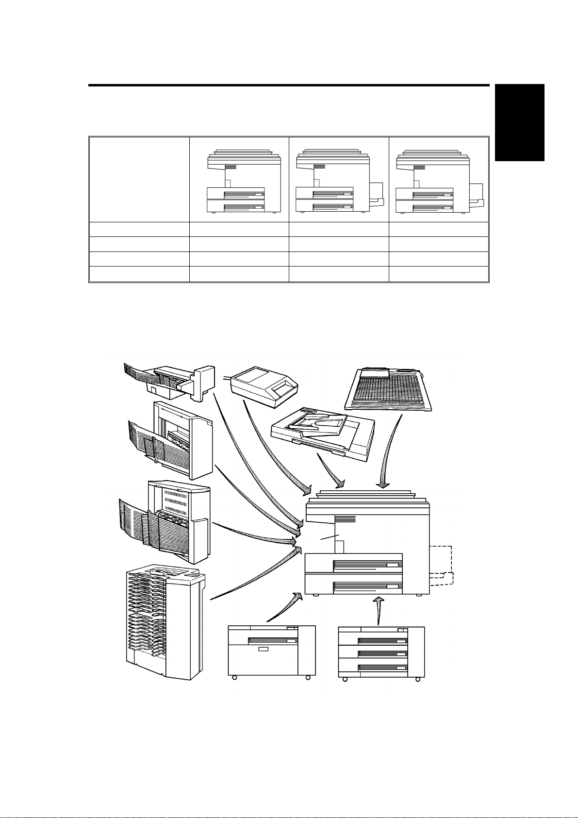
12 February 1992 MACHINE CONFIGURATION
2. MACHINE CONFIGURATION
2.1 COPIER
TYPE 1 (A069) TYPE 2 (A074) TYPE 3 (A073)
UPPER TRAY 250 DUPLEX 250
LOWER TRAY 250 250 250
LCT – 1,000 1,000
2.2 OPTIONAL EQUIPMENT
10BIN SORTER (A327)
MENU READER (A952)
EDITOR (A916)
Overall
Information
20BIN SORTER
(A423)
20BIN SORTER
(A411)
ARDF (A497)
SORTER ADAPTER
(A328)
SORTER STAPLER
(A366)
PAPER TRAY UNIT PAPER TRAY UNIT
(A325)
1-5
(A326)
Page 10

MACHINE CONFIGURATION 12 February 1992
COPIER
1 TRAY
PAPER
TRAY UNIT
SORTER
DOCUMENT
FEEDER
EDITOR (A916) x o x * **
MENU READER (A952) o o o **
COLOR DEVELOPMENT
UNIT (A337)
(A325)
3 TRAY
(A326)
10 BIN
(A327)
20 BIN MINI
(A423)
20 BIN MIDI
(A411)
20 BIN
STAPLER
(A366)
ARDF
(A497)
TYPE 1
(A069)
TYPE 2
(A074)
ooo
ooo
ooo *
ooo *
ooo * **
ooo
ooo
TYPE3
(A073)
REQUIRED OPTIONAL
EQUIPMENT
SORTER
ADAPTER
(A328)
INTERFACE
PCB
(A344)
EDITING
INTERFACE
ADAPTER
(A345)
NOTE1: * The sorter adapter is required to install the 20 bin
mini sorter, 20 bin midi sort e r or sorter stapler.
* * The I/F board is required to install the sorter stapler
or Menu Reader.
** * (1) The editing interface adapter is required to install
the editor.
(2) The editing interface adapter can be installed
independently when more precise erasing is
desired.
NOTE 2: When installing the sorter stapler, the copier must be placed
on the paper tray unit or a table of exactly the same height.
1-6
Page 11
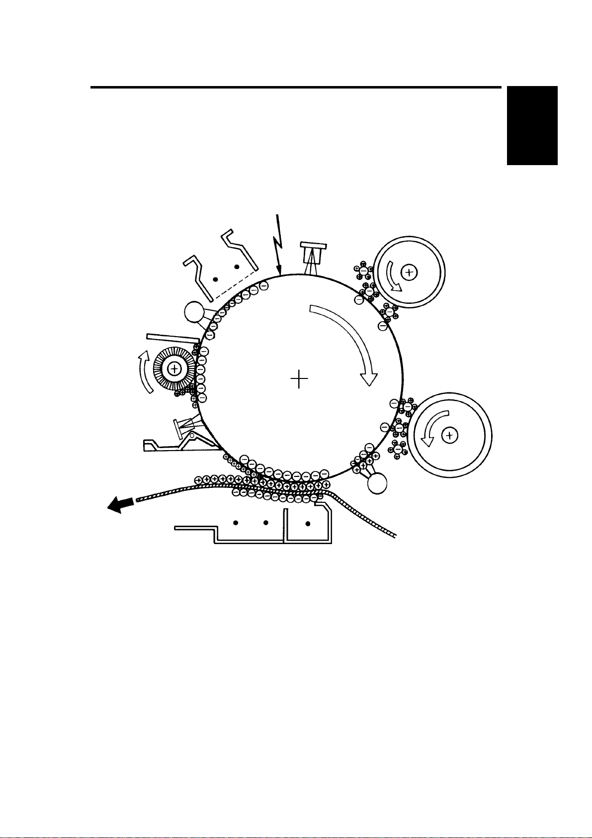
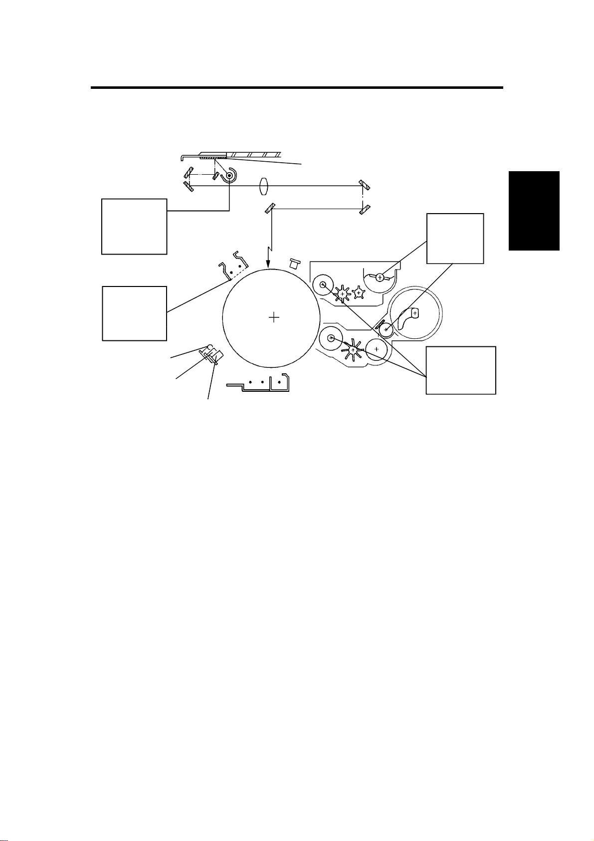
12 February 1992 COPY PROCESS AROUND THE DRUM
3. COPY PROCESS AROUND THE DRUM
2. EXPOSURE
4. DEVELOPMENT
9. QUENCHING
8. CLEANING
1. DRUM
CHARGE
3. ERASE
(COLOR)
Overall
Information
ID/V SENSORS
PICK-OFF
PAWLS
7. PAPER
4. DEVELOPMENT
(BLACK)
5. PRE-TRANSFER
LAMP
6. IMAGE TRANSFER
SEPARATION
1-7
Page 12

COPY PROCESS AROUND THE DRUM 12 February 1992
1. DRUM CHARGE
In the dark, the charge corona unit gives a uniform negative charge to the
organic photo conductive (OPC) drum. The charge remains on the surface of
the drum because the OPC layer has a high electrical resistance in the da r k.
The amount of negative charge on the drum is proportional to the negative
grid bias voltage applied to the grid plate on the charge corona unit.
2. EXPOSURE
An image of the original is reflected to the OPC drum surface via the optics
assembly. The charge on the drum surface is dissipated in direct proportion
to the intensity of the reflec te d ligh t, thus producing an electrical lat en t im ag e
on the drum surface.
The amount of remain ing char g e as a latent image on the drum de pe nds on
exposure lamp intensity controlled by the exposure lamp voltage.
3. ERASE
The erase lamp illuminates the areas of the charged drum surface that will
not be used for the copy image. The resistance of the drum in the illuminated
areas drops and the charge on those areas dissipates.
4. DEVELOPMENT
Positively charged toner is attr a c te d to the neg at ively cha r ge d ar e as of the
drum, thus developing the latent image. (The positive triboelectric charge is
caused by friction between th e car ri e r and ton er pa rticles.)
The development bias voltag e ap plie d to the deve lop m en t r oller shaf t
controls two things:
1) The threshold level if toner is attracted to the drum or toner remains on
the development roller.
2) The amount of toner to be attracted to the drum.
The higher the negative develo pment bias voltage is, the less toner is
attracted to the drum surface.
5. PRE-TRANSFER LAMP (PTL)
The PTL illuminates the drum to remove almost all the negative charge from
the exposed areas of the drum. This prevents the toner particles from being
reattracted to the drum surface during paper separation and makes paper
separation easier.
1-8
Page 13

12 February 1992 COPY PROCESS AROUND THE DRUM
6. IMAGE TRANSFER
Paper is fed to the drum surface at the proper timing so as to align the copy
paper and the develope d im ag e on the drum surface. Then, a strong
negative charge is applied to the reverse side of the copy paper, producing
an electrical force which pulls the ton er pa r ticle s fr om th e dr u m sur fa ce onto
the copy paper. At the same time, the copy paper is electrically attracted to
the drum surface.
7. PAPER SEPARATION
A strong ac corona discharge is applied to the reverse side of the copy
paper, reducing the negative charg e on the copy paper and breaking the
electrical attraction between the paper and the drum. Then, the stiffness and
the weight of the copy paper cause s it t o separ a te fr om th e drum surface.
The pick-off pawls help to separate pa pe r and drum .
8. CLEANING
Overall
Information
The cleaning brush removes tone r rem ain ing on th e dru m aft er image
transfer and the cleaning blade scrapes off all the remaining toner.
9. QUENCHING
Light from the quenching lamp electrically neutralizes the charge po tential of
the drum surface.
1-9
Page 14
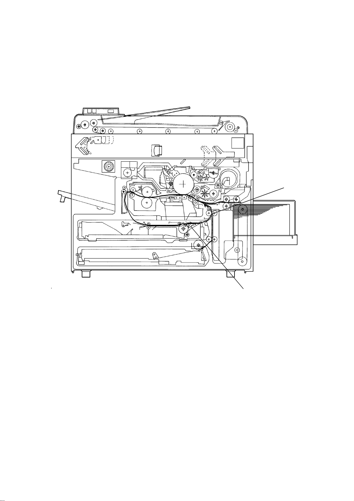
MECHANICAL COMPONENT LAYOUT 12 February 1992
4. MECHANICAL COMPONENT LAYOUT
111098765
4
3
12
13
14
2
1
424142
40
39
38
37
36
35
34
33
32 31
1. 3rd Mirror
2. 2nd Mirror
3. 1st Mirror
4. Exposure Lamp
5. Lens
6. Cleaning Brush
7. Quenching Lamp
8. Cleaning Blade
9. Change Corona Unit
10. OPC Drum
11. 6th Mirror
12. Erase Unit
13. 4th Mirror
14. 5th Mirror
15. Color Development Unit
16. Black Development Unit
17. Black Toner Supply Unit
18. Pre-Transfer Lamp
19. Feed Roller
20. Pick-up Roller
21. Separation Roller
30
15
29 28 27
26 25 24 23
22. Large Capacity Tray
23. Relay Rollers
24. Registration Rollers
25. Paper Tray Feed Roller
26. Friction Pad
27. Turn Gate
28. Duplex Friction Roller
29. Duplex Feed Roller
30. Transfer & Separati on Coron a Unit
31. Jogger Fences
32. End Fence
33. Lower Paper Tray
34. Entrance Rollers
35. Duplex Tray
36. Pressure Roller
37. Pick-off Pawls
38. Hot Roller
39. Junction Gate
40. Hot Roller Strippers
41. Transport Fan
42. Fusing Exhaust Fan
16
17
18
19
20
21
22
1-10
Page 15
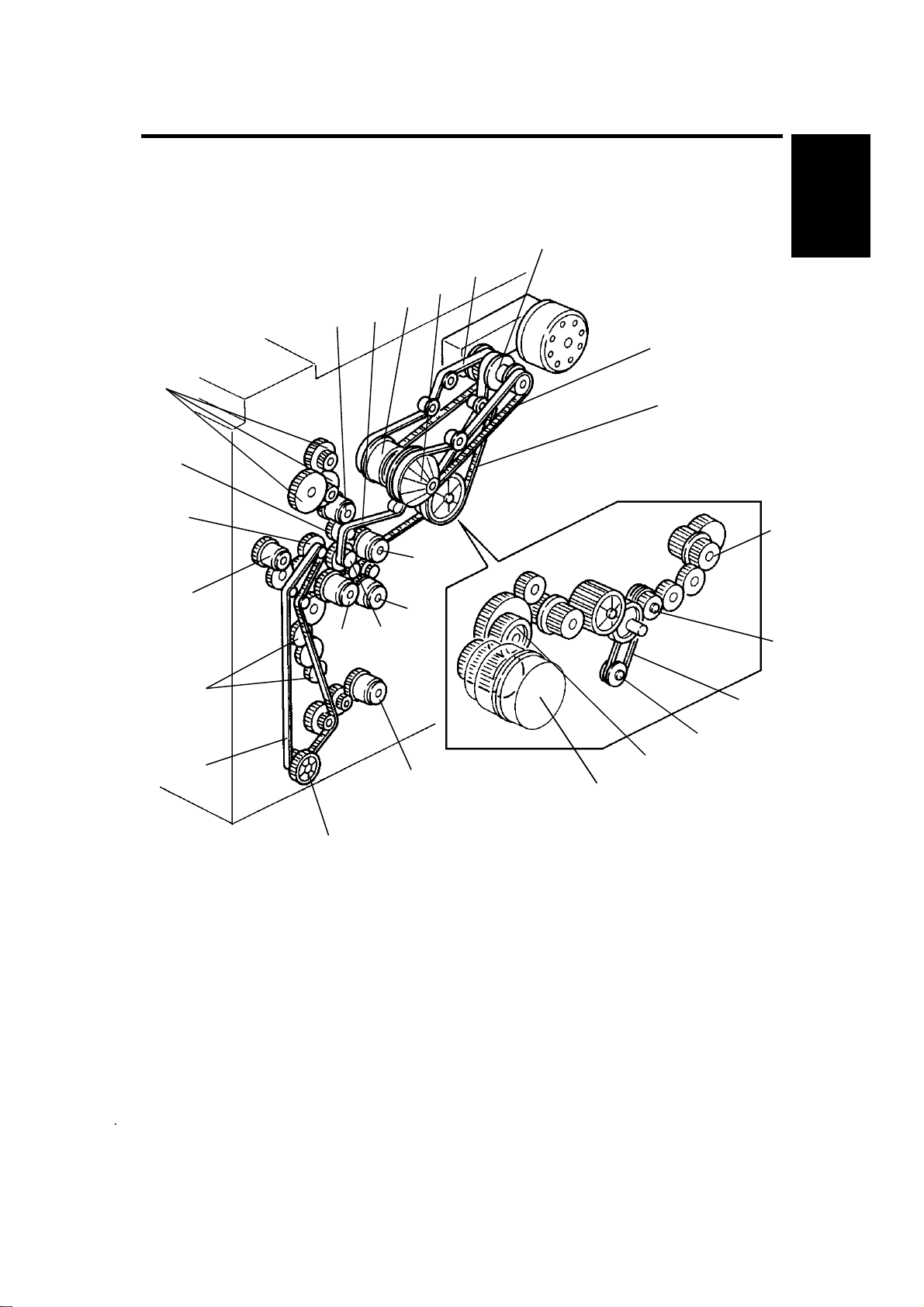
12 February 1992 DRIVE LAYOUT
5. DRIVE LAYOUT
21
20
19
18
22
13
23
12
24
11
10
25
26
1
2
Overall
Information
5
6
17
16
7
8
9
14
134
1015
1-11
Page 16
DRIVE LAYOUT 12 February 1992
1: Main Motor Pulley
3: Fusing Drive Belt 2: Drum Drive Belt
4: Drive Distribution
Gear/Pulley
23: Drive Distribution Belt Cleaning drive Gear 9: Fusing Unit Drive
12: Drive Distribution
Gear/Pulley
25: Drum Drive Pulley 24: Development Drive
Drum Development Unit
Cleaning Unit Fusing Unit
20: Toner Supply
Drive Gear/Pulley
22: Toner Supply CL
Gear
26: Development Drive
Belt
CL Pulley
Gear
6: Copier Exit
Roller Gear
7: Duplex Transport
Drive Belt
19: Paper Feed Drive
Gear/Pulley
16: Paper Feed Drive
Belt
14: Lower paper Feed
CL Gear
21: Development Unit
Shift Gears
10: Registration CL Gear
11: Upper Paper Feed CL
13: Feed Relay CL Gear
17: Relay Roller Gears
18: By-pass Feed CL
Gear
15: Tray Unit drive
Gear
8: Duplex Transport
Roller Pulley
5: Sorter Adapter Gears
1-12
Page 17
12 February 1992 PAPER PATH
6. PAPER PATH
6.1 NORMAL COPYING
[D]
[E]
[C]
[B]
[A]
Overall
Information
[A]
Paper feed begins from the LCT or paper tray unit paper feed stations. The
copy paper then follows one of tw o pa th s inside the copie r . The pat h fo llowe d
depends on which mode the operator has selected. For copy processing, all
sheets follow the same path from the paper feed mechanism [A] through the
registration [B], T & S corona [C], and fusing unit [D]. After that, normal
copies are delivered to the copy tra y [E], however, 2 sided copies and
overlay copies are diverted for further processing.
1-13
Page 18
PAPER PATH 12 February 1992
6.2 MULTIPLE 2-SIDED COPYING
[H]
[G]
[A]
[B]
[C]
[F]
Paper that is A4, B5, and 8
[E]
" X 11" sideways can be used for multiple
1/2
[D]
2-sided copying. In this mode the junction gate [A] directs sheets exiting the
fusing unit to the duplex tray entrance [B]. After that, all sheets follow the path
through the entrance rollers [C], and the turn gate [D]. The turn gate directs
paper through the duplex feed mechanism [E] to the duplex tray [F]. After all
sheets are stacked in the duplex tray, these sheets follow the path thr ough
the duplex feed mechanism and relay rollers [G] to the registration rollers [H].
After that, these sheets follow the same pat h as normal cop ying fr om th e
registration rollers to the copy tray.
1-14
Page 19
12 February 1992 PAPER PATH
6.3 SINGLE 2-SIDED COPYING
[D]
Overall
Information
[A]
[B]
[C]
Any sheet up to A3\11" x 17" but except for A4, B5, or 8
" X 11" sideways
1/2
can be used for single 2-sided copying. In this mode, the sheet follows the
same path as in multiple 2-sided copying to the duplex tray. However, the
end fence [A] of the duplex tray lowers. The sheet advances over the lowered
end fence. The sheet is stopped by the friction between the duplex feed and
friction rollers [B,C]. It is directed to the relay rollers [D] by the reversed
duplex feed roller. It stays there once. After that, the sheet follows the same
path as in multiple 2-sided copying from the relay rollers to copy tray.
1-15
Page 20
PAPER PATH 12 February 1992
6.4 SINGLE IMAGE OVERLAY COPYING
[B]
[A]
In this mode, the sheet follows the same path as in multiple 2-sided copying
to the turn gate [A]. The turn gate directs the sheet to the relay rollers [B].
The sheet stays there once. After that, the sheet follows the same path as in
multiple 2-sided copying from the relay rollers to the copy tray.
1-16
Page 21

12 February 1992 ELECTRICAL COMPONENT DESCRIPTION
7. ELECTRICAL COMPONENT DESCRIPTION
Refer to the electrical component layout on the reverse side of the Point to
Point (Water proof pap er) fo r symbols an d ind ex nu m ber s.
Symbol Name Function Index No.
Motors
M1 Main Drives the main unit components. 1
Overall
Information
M2 Exhaust blower Blows the ozone built up around the charge
section through the ozone filter.
M3 Upper tray lift
(non-duplex
machine only)
M4 Lower tray lift Raises the bottom plate in the lower paper
M5 Transport fan Provides air flow to the transport section so
M6 Fusing exhaust
fan
M7 Scanner drive Drives the 1st and 2nd scanners (dc
M8 3rd scanner drive Drives the 3rd scanner (dc stepper). 75
Raises the bottom plate in the upper paper
tray.
tray.
that paper is held on the transport guide.
Also the air flow isolates the toner
collection tank from fusing heat.
Provides air flow to the charge corona
section as well.
Removes the heat from around the fusing
unit.
stepper).
6
31
28
65
66
67
M9 Optics cooling fan Removes heat from the optics unit. 77
M10 Lens drive Positions the lens. 100
M11 Duplex feed
(duplex machine
only)
M12 Jogger (duplex
machine only)
M13 LCT lift Lifts up and lowers the LCT bottom plate. 79
Drives the feed roller and moves the
bottom plate up and down (24 V dc
stepper).
Drives the jogger fences to square the
paper stack in the duplex tray (dc stepper).
1-17
103
107
Page 22

ELECTRICAL COMPONENT DESCRIPTION 12 February 1992
Symbol Name Function Index No.
Circuit Board
PCB1 dc power supply Drives the exposure and fusing lamps and
rectifies 100 Vac or 220/230/240 Vac input
and outputs dc voltages.
PCB2 Main control Controls all copier functions both directly
and through the other control boards.
PCB3 Scanner motor
control
PCB4 Main motor
control
PCB5 Operation panel Controls the LED matrix, and monitors the
PCB6 ADS sensor Senses the background density of the
PCB7 High voltage
supply - CTBG
PCB8 High voltage
supply - D
Controls the speed of the scanner drive
motor.
Controls the rotation of the main motor. 71
key matrix.
original.
Supplies high voltage for the charge
corona, grid bias, transfer corona, and
development bias.
Supplies high voltage for the separation
corona.
44
10
69
93
90
9
8
PCB9 PTL/QL stabilizer Provides high voltage for the quenching
and pre-transfer lamps.
PCB10 Duplex control
(duplex machine
only)
PCB11 LCT interface
(LCT machine
only)
PCB12 Guidance display
control (duplex
machine only)
PCB13 Guidance display
(duplex machine
only)
Controls the rotation of the duplex feed
motor.
Interfaces the LCT control signal between
the main control board and the LCT.
Controls the guidance display board. 92
Displays guidance for machine operation. 94
73
106
80
1-18
Page 23

12 February 1992 ELECTRICAL COMPONENT DESCRIPTION
Symbol Name Function Index No.
PCB14 Interface - type
G (option for
sorter stapler
and menu
reader)
PCB15 Nose filter
(230 V machine
only)
Switches
SW1 Upper paper size
- 1 (non-duplex
machine only)
SW2 Upper paper size
- 2 (non-duplex
machine only)
SW3 Upper paper size
- 3 (non-duplex
machine only)
SW4 Upper paper size
- 4 (non-duplex
machine only)
Interfaces the sorter stapler and menu
reader with the main control board.
Removes electrical noise 35
Determines what size paper is in the upper
paper tray.
Determines what size paper is in the upper
paper tray.
Determines what size paper is in the upper
paper tray.
Determines what size paper is in the upper
paper tray.
16
2
3
4
5
Overall
Information
SW5 Lower paper size
- 1
SW6 Lower paper size
- 2
SW7 Lower paper size
- 3
SW8 Lower paper size
- 4
SW9 Color detection Detects if color development unit is set or
SW10 Exit cover
(Duplex machine
only)
SW11 Platen cover Informs the CPU when the platen cover is
Determines what size paper is in the lower
paper tray.
Determines what size paper is in the lower
paper tray.
Determines what size paper is in the lower
paper tray.
Determines what size paper is in the lower
paper tray.
not and which color toner development unit
is installed.
Cuts the ac power line. 64
closed.
36
34
33
32
13
88
1-19
Page 24

ELECTRICAL COMPONENT DESCRIPTION 12 February 1992
Symbol Name Function Index No.
SW12 Front door safety Cuts the ac power line through RA1 and
detects if the front door is open or not.
SW13 Main Supplies power to the copier. 95
SW14 LCT cover - 1
(LCT machine
only)
SW15 LCT cover - 2
(LCT machine
only)
SW16 LCT down (LCT
machine only)
Lamps
L1 Quenching Neutralizes any charge remaining on the
L2 Pre-transfer Reduces the charge on the drum surface
Detects if the LCT cover is open or not. 83
Cuts the dc power line of the LCT lift motor. 84
Sends a signal to the CPU to lower the LCT
bottom plate.
drum surface after cleaning.
before transfer.
91
85
47
49
L3 Fusing Provides heat to the hot roller. 60
L4 Exposure Applies high intensity light to the original
exposure.
L5 Erase Eliminates the charge for unnecessary
areas of the image on the drum surface
before exposure.
Magnetic
Clutches
MC1 Development
drive
MC2 Toner supply Drives the toner supply roller. 14
MC3 By-pass feed Starts paper feed from the by-pass feed
MC4 Feed relay Drives the relay rollers. 19
MC5 Registration Drives the registration rollers. 20
Drives the development roller. 11
table or LCT.
99
48
17
1-20
Page 25

12 February 1992 ELECTRICAL COMPONENT DESCRIPTION
Symbol Name Function Index No.
MC6 Upper paper
feed (non-duplex
machine only)
MC7 Lower paper feed Starts paper feed from the lower paper tray. 24
Solenoids
SOL1 Development
unit change
SOL2 Pick-up roller Picks paper up from the by-pass feed table
SOL3 Duplex tray lock
(duplex machine
only)
SOL4 Upper tray lock
(non-duplex
machine only)
SOL5 Lower tray lock Locks the lower paper tray in the main
Starts paper feed from the upper paper tray. 22
Changes the position of the black
development unit and color development
unit.
or LCT.
Locks the duplex tray in the main copier. 29
Locks the upper paper tray in the main
copier.
copier.
12
18
39
37
Overall
Information
SOL6 Junction gate
(duplex machine
only)
SOL7 Duplex turn gate
(duplex machine
only)
Sensors
S1 By-pass feed
table
S2 Upper tray set
(non-duplex
machine only)
S3 Lower tray set Detects if the lower paper tray is set or not. 26
S4 By-pass feed
paper end
S5 Upper tray paper
end (non-duplex
machine only)
Moves the junction gate to direct copies to
the duplex tray or to the paper exit.
Moves the duplex turn gate to direct copies
to the duplex tray or to the relay rollers.
Detects if the by-pass feed table is open or
closed.
Detects if the upper paper tray is set or not. 21
Informs the CPU that there is no paper in
the by-pass feed table.
Informs the CPU when the upper paper tray
runs out of paper.
43
105
15
53
23
1-21
Page 26

ELECTRICAL COMPONENT DESCRIPTION 12 February 1992
Symbol Name Function Index No.
S6 Lower tray paper
end
S7 Upper tray upper
limit (non-duplex
machine only)
S8 Lower tray upper
limit
S9 Lower relay Detects the lead edge of paper from the
S10 Upper relay Detects the lead edge of paper from the
S11 Registration Detects the lead edge of paper to
Informs the CPU when the lower paper tray
runs out of paper.
Detects the upper position of the paper
stack in the upper tray to stop the upper lift
motor.
Detects the upper position of the paper
stack in the lower tray to stop the lower lift
motor.
lower paper tray to determine the stop
timing of the lower paper feed clutch and
detects misfeeds.
upper paper tray to determine the stop
timing of the upper paper feed clutch and
detects misfeeds.
determine the stop timing of the feed relay
clutch and detects misfeeds.
25
30
27
51
50
52
S12 Image density
(ID)
S13 V Detects the VR and VL patterns. 58
S14 Fusing exit Detects misfeeds. 62
S15 Junction gate
(duplex machine
only)
S16 Scanner H.P. Informs the CPU when the 1st scanner is at
S17 Lens H.P. Informs the CPU when the lens is at the
S18 Platen position Informs the CPU when the platen cover is
S19 3rd scanner H.P. Informs the CPU when the 3rd scanner is in
Detects the density of the ID sensor pattern
on the drum to control the toner density.
Detects misfeeds. 63
the home position.
full-size position.
positioned. When the angle between, the
platen cover and the exposure glass is
about 30 degrees.
the full size position.
57
68
72
74
76
S20 Original length Detects the original length. 89
1-22
Page 27

12 February 1992 ELECTRICAL COMPONENT DESCRIPTION
Symbol Name Function Index No.
S21 Original width Detects the original width. 96
S22 Duplex entrance
(duplex machine
only)
S23 Duplex turn gate
(duplex machine
only)
S24 Duplex paper
end (duplex
machine only)
S25 Jogger H.P.
(duplex machine
only)
S26 LCT paper end
(LCT machine
only)
S27 LCT lower limit
(LCT machine
only)
Detects misfeed. 109
Detects the trail edge of paper to determine
the reverse timing of the duplex motor and
detects misfeed.
Detects copy in the duplex tray. 102
Detects if the jogger fences are at home
position.
Informs the CPU when the LCT runs out of
paper.
Sends signal to CPU to stop lowering the
LCT bottom plate.
101
108
82
81
Overall
Information
S28 LCT upper limit
(LCT machine
only)
Heaters
H1 Drum Turns on when the main switch is off to
H2 Optics
anti-condensation
(option)
H3 Upper tray
(option)
H4 Lower tray
(option)
Thermistor
TH1 Drum Monitors the temperature around the drum. 56
TH2 Fusing Monitors the temperature of the hot roller. 59
Sends signal to CPU to stop lifting up the
LCT bottom plate.
prevent moisture around the drum.
Turns on when the main switch is off to
prevent moisture from forming on the optics.
Turns on when the main switch is off to
keep paper dry in the upper paper tray.
Turns on when the main switch is off to
keep paper dry in the lower paper tray.
78
54
97
55
87
1-23
Page 28

ELECTRICAL COMPONENT DESCRIPTION 12 February 1992
Symbol Name Function Index No.
TH3 Optics Monitors the temperature of the optics
cavity.
TH4 Duplex motor
(duplex machine
only)
Thermofuse
TF1 Fusing Provides back-up overheat protection in the
Thermoswitch
TS1 Optics Provides overheat protection in the optics
Noise filter
NF1 Removes electrical noise. 40
Fuse
FU1 Main (115 V
machine only)
Monitors the temperature of the duplex
motor.
fusing unit.
unit.
Provides back-up high current protection in
the electrical components.
98
104
61
70
42
FU2 Sorter line (115
V machine only)
FU3 DF line (115 V
machine only)
Circuit Breaker
CB1 (230 V machine
only)
Relay
RA1 Main power Controls main power. 45
Transformer
TR1 Main Steps down the wall voltage to 100 V ac. 38
Counter
CO1 Total Keeps track of the total number of copies
Provides back-up high current protection in
the electrical components of the sorter.
Provides back-up high correct protection in
the electrical components of the ARDF.
Provides back-up high current protection in
the electrical components.
made.
46
7
41
86
1-24
Page 29

SECTION 2
DETAILED SECTION
DESCRIPTIONS
Page 30
12 February 1992 PROCESS CONTROL
1. PROCESS CONTROL
1.1 OVERVIEW
ID Sensor Pattern
V Sensor Pattern
Exposure
Lamp
Voltage
(Color)
Grid
Bias
Voltage
Toner
Supply
Detailed
Descriptions
Drum Thermistor
(Black)
ID Sensor
V Sensor
Development
Bias
Voltage
As seen in section 1 the copy process around the drum and the copy image
(image and background density) are controlled by many factors.
On this copier, the following items are controlled during the copy process to
maintain good copy quality:
The exposure lamp voltage of the optics section
The grid bias voltage of the drum charge section
The development bias voltage and to ner supply of the development
section
The items above use the following electrical components:
The operation panel (manual ID selectio n and reproduction ratio), ADS
sensor, ID sensor, V sensor, drum thermistor, paper size switches,
color detection switches, and RAM board (drum rotation time and SP
mode data)
Refer to the process control table in the supplement sheet bag for the details
on which electrical component controls which controlled item.
In the following sections, we will explain briefly how the major electrical
components are controlled in the copy process.
2-1
Page 31

PROCESS CONTROL 12 February 1992
1.2 ID SENSOR CONTROL
Sensor
Pattern
Original Lead Edge
Original
ON OFF ON OFF
A B C
RAM Clear
1234567891011121314 202122
Toner Density Detection Toner Density Detection Toner Density
D E
1st
Leading Edge Erase
Detection
ID Sensor
Pattern
2nd 3rd
Low Toner Density
Toner Supply Timing
Toner Add
Toner Supply Clutch ON
(10 times)
Detection
Development
Bias
Detection
1.2.1 Overview
An ID (Image Density) sensor is used to control toner supply.
The sensor is located on the drum unit, under the cleaning unit. Placing the
sensor under the cleaning unit, instead of the development unit, reduces the
risk of scattered toner getting on the sensor.
The CPU checks toner density through the ID sensor by directly sensing the
image density on the drum. This is done every 10 copy cycles (every 5 copy
cycles for the color development unit). Turning the main switch off and on has
no effect because the count is stored in RAM. If the drum initialization is
performed (SP mode #66) or the RAM is cleared (SP mode #99), the CPU
starts counting for the toner density check from the beginning of the first copy
cycle.
The ID sensor pattern (black) is stuck on the operator side of the bott om of
the left scale bracket. During the check cycle, the ID sensor pattern is
exposed prior to exposure of the original.
2-2
Page 32

12 February 1992 PROCESS CONTROL
After the ID sensor pattern is developed, the ID sensor checks the pattern’s
reflectivity and the CPU notes it. If the reflected light is too strong, indicating
toner density is too low, toner is added to the development unit.
The toner is not added all at once. The CPU energizes the toner supply
clutch solenoid for the proper amount of time to add a calculated amount of
toner over the next 10 copy cycles (5 copy cycles for color toner).
Such toner supply control through the ID sensor is called a detect supply
mode. On this copier, this mode is used to control both black and color toner
supply.
Detailed
Descriptions
2-3
Page 33

PROCESS CONTROL 12 February 1992
1.2.2 ID Sensor Output
VSG = 4.0 ± 0.2
1/10 VSG = 0.4
(V)
LED
ON
VSG
0
Sensor
Bare
pattern
drum
LED
ON
VSP
VSG
1/10 VSG
(T)
VSP
Low image density
High image density
0
When in the toner density check cycle, the CPU receives two voltage values
directly from the ID sensor: Vsg and Vsp. Vsg is the voltage value for the
area of the drum made bare by the erase lamp unit before the ID senso r
pattern is exposed. Vsp is the voltage value for the developed ID sensor
pattern. The CPU compares these two values to monitor the image densit y
on the drum and with this controls the toner supply.
[Standard setting ] 0 to 500 copies Over 500 copies
Black toner – 220 V – 200 V
Red/Blue toner – 200 V – 180 V
Green toner – 240 V – 220 V
Vsg is the reference voltage of the ID sensor output and is automa tica lly
adjusted to 4V whenever SP mode #54 is called.
The development bias for the ID senso r pat te r n is fi xed for each toner color.
This is to avoid any influence from the m an ual ID level set tin g on ton er
density control. (See chart.)
2-4
Page 34

12 February 1992 PROCESS CONTROL
Vsg
Vsp
[Black Toner]
100% (4.0 V)
Low Density
10% (0.4 V)
High Density
Vsg
Vsp
[Color Toner]
High Density
(1) Detect supply mode
In the detect supply mode toner will be supplied under the following
conditions:
Black toner...........................Vsp/ Vsg x 100 ≥ 10
Color toner...........................Vsp/ Vsg x 100 ≥ 25
(2) Fixed supply mode
A fixed amount of toner is supplied every copy cycle when the fixed
supply mode is selected (when the data of SP mode #30 is "1").
On this copier, this mode can be selected only for black toner.
The CPU monitors Vsp and Vsg once every 10 copy cycles even in the
fixed supply mode.
To avoid over toning, the CPU stops toner supply when Vsp becomes
1/10 Vsg or less.
100% (4.0 V)
Low Density
25% (1.0 V)
Detailed
Descriptions
2-5
Page 35

PROCESS CONTROL 12 February 1992
4.0 V
2.5 V
Vsg
Vsp
[Vsg abrormal]
Vsg
Vsp
[Vsp abnormal]
(3) ID Sensor Abnormal Conditions
The following ID sensor abnormal conditions apply to both the detect and
fixed supply modes.
a. Vsg abnormal
When Vsg falls under 2.5V, the CPU stops the toner supply and
continues the ID sensor patt ern detection (every 10 copies for bla ck
and every 5 copies for color). If this abnormal value of Vsg is detected
5 times in a row under this condition (without any toner supply), the
CPU makes the call service indicator blink. Then the CPU shifts the
toner supply to the abnormal fixed supply mode. But in this condition
the CPU never stops the toner supply as it does to avoid overtoning in
the normal fixed supply mode.
b. Vsp abnormal
When [Vsp/Vsg X 100] goes to 50 or more, the CPU changes the toner
supply amount to the ID sensor abnormal level and continues toner
supply and ID sensor pattern detection. If this abnormal value of Vsp is
detected 5 times in a row, the CPU makes the call service indicator
blink. Then the CPU shifts the toner supply to the abnormal fixed
supply mode, as it does under a Vsg ab no r mal con dit ion .
100% (4.0 V)
50% (2.0 V)
NOTE: The CPU continues the ID sensor pattern detection even under
the ID sensor abnormal condition s .
For both black and color toners, if Vsg and Vsp return to the
normal range at any of the subsequent toner density check
cycles, the CPU will return the toner supply control to normal.
2-6
Page 36

12 February 1992 PROCESS CONTROL
1.3 VR PATTERN CONTROL
1.3.1 Overview
(V)
Drum
residual
voltage
Copy volume
(V)
Drum
potential
Light intensity
During the OPC drum’s life, drum residual voltage gradually increases due to
electrical fatigue. This may cause dirty backgrounds on copies. The V sensor
is used to avoid this problem.
The V sensor is located on the drum unit, on the same frame as the ID
sensor. The ID sensor is located on the non-operator side and the V sensor
is on the operator side.
The CPU checks the drum residual voltage through the V sensor by directly
sensing the VR pattern on the drum surface. This VR pattern detection is
performed after the drum initial setting (SP mode #66). After this, the CPU
will do one VR pattern detection every 200 copie s f or th e ne xt 2,000 copies,
and every 1,000 copies after that. Also when VR data correction (See 1.5
Drum Temperature Control) is applied and the drum temp erature goes over
25°C, this detection is performe d.
Detailed
Descriptions
According to the data of the VR pattern detection, the CPU ap plies V
correction to the grid bias volt ag e an d th e de velopment bias voltage.
2-7
R
Page 37

PROCESS CONTROL 12 February 1992
1.3.2 VR Pattern Detection
Image
0V Bias
Non-image
Fixed Bias
Vrg
VR Pattern
V Sensor
Vrp
The VR pattern is made on the drum befo r e th e original latent image, as in
the case of the ID sensor pattern.
During VR pattern detection, the drum surface is charged with a fixed grid
bias voltage: – 500V + VG correction (see 1.6 Drum Rotation Time Control).
At the same time all the blocks of the erase lamp unit turn on to illuminate this
charged area of the drum.
The exposed area of the drum is develop ed with a fixed bias voltage for
non-image area: – 160V + VR correction + VR Data correction (See 1.5 Drum
Temperature Control) + Bl ack Bia s cor rect ion (SP mode #37). The V sensor
checks the reflectivity of the bare area of the drum and this sensor output
voltage is called Vrg. (The meaning of Vrg is the same as that of Vsg
detected by the ID sensor.)
Just next to this bare drum area, th e dr u m is develo pe d with VR pattern bias
voltage (0V). If there is residual voltage on the drum, this are a of the drum
will attract some toner, making a VR pattern. The V sensor checks the
reflectivity of the VR pattern and this sensor output voltage is called Vrp.
The CPU notes the ratio, Vrp/Vrg. This VR pattern check is done 5 times in a
row during the copy cycle (among 5 copies) and the CPU takes their average.
During the 5 VR pattern check cycles, if color copies are made, or if a toner
density check is done, the CPU skips the VR pattern check and will do it in
the next copy cycles.
If an ID sensor abnormal conditio n occu r s, the CPU does not perform the V
R
pattern detection because toner density may not be proper.
2-8
Page 38

12 February 1992 PROCESS CONTROL
1.3.3 VR Correction
VR level Vrp/Vrg x 100(%)
0100~84
Grid bias correction
voltage
0 V
±
Development bias
correction voltage
0 V
±
1 83~58 – 40 V – 40 V
2 57~41 – 80 V – 80 V
3 40~28 – 12 0 V – 120 V
4 27~0 – 16 0 V – 160 V
When calling SP mode #54, the reference voltage of the V sensor output Vrg
is automatically adjusted to 4V at th e sam e tim e as Vsg is adjust ed .
The grid bias voltage and the de velo pm e nt bias voltage are corrected (V
R
correction) according to the ratio between Vrp and Vrg as shown in the above
table.
(ex. If there is no residual voltage on the drum, Vrp=4V and Vrg=4V. Then
the proportion is: Vr p/Vrg x 100 = 4/4 x 100 = 100%)
When the drum residual voltage increases, th e VR pattern becomes darker.
The value of Vrp decreases and also the Vrp/Vrg ratio decreases. Then the
CPU increases the negative development bias voltage to prevent a dirty
background, and simultaneo usly incr e ase s the negat i ve gr id bias voltage to
prevent low image density.
Detailed
Descriptions
,
2-9
Page 39

PROCESS CONTROL 12 February 1992
1.4 VL PATTERN CONTROL
1.4.1 Overview
I
D Sensor Pattern
V
Pattern
L
DC
PSU
Main
Board
(V)
Drum
Potential
V Sensor
Exposure lamp voltage
(V)
Dirty optics or deterioration of the exposure lamp decreases the int ensity of
the light that reaches the drum via th e op tics cavity. As more copies are
made during the drum’s life, the pho to cond uct i ve laye r get s wor n and dr u m
sensitivity drops. The drum sensitivity also drops under low temperature
condition.
VL pattern control is performed on this copier to prevent dirty backgrounds
caused by the factors mentioned above. The V sensor is also used for V
L
pattern control as well as for VR pattern control.
The VL pattern (light gray) is located on the non-operator side of the bottom
of the left scale bracket. When a copy job fi nish es in VL pattern detection
timing, the exposure lamp stays on for ab ou t 6 seco nd s while at the home
position. The VL pattern is lit and a latent image of it is made on the drum.
After this image is developed, its reflectivity is checked by the V sensor. The
CPU notes the strength of reflectivity, and if the reflected light is too weak,
the exposure lamp voltage is increased.
2-10
Page 40

12 February 1992 PROCESS CONTROL
1.4.2 VL Pattern Detection
Main SW on
data
V
R
correction
done ?
Y
Drum Temp.
> 25°C
N
N
Programmed
copy
interval ?
Y
N
VL Pattern
Y
150 mm
pattern detection
V
R
Detailed
Descriptions
N
Is copy
Job completed ?
20 mm
Y
20 mm
pattern detection
V
L
Vdat = Vlp/Vlg
VL pattern detection is done after VR pattern detection, but unlike VR pattern
detection it is done after the cop y job is fi nish ed . This m ea ns af te r the drum
initial setting (SP mode #66), ever y 20 0 cop i es fo r the fir st 2,000 copies,
every 1,000 copies af te r excee din g 2,000 copies, and when the dr um
temperature go es ove r 25°C un de r t he VR data correction condition.
When VL pattern detection starts, the exposure lamp turns on, the main
motor stays, on together with other fan motors, to rotate the drum. The
charge corona, grid bias, all the blocks of the erase lamp, the pre-transfer
lamp, and the quenching lamp turn on.
After about one revolution of the drum, the appropriate blocks of the erase
lamp turn off and on to make a VL pattern (20 x 20 mm) on the drum surface.
The drum surface is developed with non-image area bias for both the bare
drum and VL pattern.
The V sensor checks the reflectivity of the bare drum (Vlg) and that of the V
pattern (Vlp). The CPU calculates the ratio between Vlp and Vlg (Vlp/Vlg).
The VL pattern is made 4 times with 150 mm distance between each pattern .
The CPU takes the average of Vlp/Vlg (=Vdat).
2-11
L
Page 41

PROCESS CONTROL 12 February 1992
When the drum initial setting (SP mode #66) is performed and more than 7
black copies are made, the init ial VL detection is performed at the end of the
copy job and the CPU stores the VL reference value (initial Vlp/Vlg = Vref) in
memory. ID sensor patter n de te ction and VR pattern detection is done prior to
this initial VL detection.
ID sensor pattern an d VR pattern detections are performed when blac k
copies are made even in the SP mode. However, VL pattern detection is
performed when a black copy is made in enlarge or full size mode and no t in
the SP mode.
1.4.3 VL Correction
VL Level (%)
Lamp correction
voltage
151~ –1 V
101~150
±
0 V
0~100 +1 V
The V sensor output is automatically adjusted to 4V (for Vlg=Vrg) by calling
SP mode #54 as we mentione d in 1. 3.3 VR Correction.
When the VL pattern detection is performed during the operation, the CPU
compares the Vdat with the Vref. According to the ratio be twe en Vda t an d
Vref, the CPU applies the voltage correction to the exposure lamp (V
L
Correction) as shown in the above table.
Vdat/Vref x 100 = VL level (%)
The exposure lamp voltage for VL pattern detection depe nd s on all pr e viou s
correction factors, and the new VL correction factor is added to them. This
result is then applied to the exposure lamp voltage till the next VL pattern
detection.
2-12
Page 42

12 February 1992 PROCESS CONTROL
1.5 DRUM TEMPERATURE CONTROL
1.5.1 Overview
(V)
Drum
potential
Exposure lamp voltage
(V)
(V)
Drum
potential
Light intensity
Under low temperature conditions drum sensitivity drops and dru m residu al
voltage increases. This is a characteristic of the drum and may cause dirty
backgrounds on copies.
To compensate for this, a drum thermistor is installed on the ID sensor board
to monitor the temperature around the drum.
When the main switch is turned on, the CPU checks the temperature through
the drum thermistor. I f th e te m per ature is 25°C or less, the CPU applies
appropriate correctio ns to the exposure lamp voltage (low te m p. corr ect ion ) ,
to the grid bias voltage (VR data correction), and to the development bias
voltage (VR data correction).
Detailed
Descriptions
When the tempera tu r e goes over 25°C, the VR pattern detection and V
L
pattern detection are performed and the above corrections are canceled.
If the temperature is alread y over 25 °C when the ma in switch is turne d on , no
correction is applied.
2-13
Page 43

PROCESS CONTROL 12 February 1992
Low Temp.
correction
Exposure lamp
voltage
Grid bias voltage
VR Data correction
Development bias
voltage
Over 25°C No correction No correction No correction
25°C or lower Lamp voltage + 1V VR level + 1 VR level + 1
1.5.2 Low Temp. Correction
When a correction is required under low temperature conditions, the CPU
increases the exposure lamp voltage by 1V.
1.5.3 VR Data Correction
When the low temp. correction is applied, VR data correction is applied
simultaneously. The VR correction level for both the grid bias voltage and the
development bias voltage is stepped up by 1. This means the negative
voltage for the charge grid and the development bias is increased by 40V.
2-14
Page 44

12 February 1992 PROCESS CONTROL
1.6 DRUM ROTATION CONTROL
(V)
Drum
potential
Drum rotation time
(H)
Detailed
Descriptions
(V)
–600
–550
–500
–450
Grid bias
voltage
–500
0 1 2
VG Correction for Sensor
Pattern
–580
–560
–540
–520
37 63 88~(H)
Drum rotation time
(V)
–850
–800
–750
–700
Grid bias
voltage
–745
0 1 2
VG Correction for Image
–805
–785
–765
37 63 88~(H)
Drum rotation time
1.6.1 Overview
During the OPC drum’s life the photo conductive layer gets worn and this
causes a drop in drum sensitivity and a decrement in the drum potential after
the drum charge.
The CPU keeps track of the drum rotation time (main motor on time) that
corresponds to the wear of the drum surface. The grid bias voltage is
increased at set intervals (VG correction).
–825
1.6.2 VG Correction
If drum potential decreases after the drum charge, the ID sensor pattern on
the drum becomes lighter, causin g hig he r ton er con c en tr a tio n in th e
developer. Also, copy image density becomes slightly lighter.
To control toner density properly and to keep copy image density, drum
potential is maintained by increments of the grid bias voltage at set intervals.
(See graph above)
2-15
Page 45

PROCESS CONTROL 12 February 1992
The drop of drum sensitivity due to th e dr u m wear is com pe nsated by V
L
correction. VL correction is performed more often than VG correction,
therefore, VG correction is not applied to the exposure lamp voltage, only to
the grid bias voltage.
2-16
Page 46

12 February 1992 DRUM
2. DRUM
2.1 OPC DRUM CHARACTERISTICS
An OPC has the characteristics of:
1. Being able to accept a high negative electrical charge in the dark. (The
electrical resistance of a photo c on du cto r is high in the absence of light.)
2. Dissipating the electrical charge when exposed to light. (Exposure to light
greatly increases the conductivity of a photoconductor.)
3. Dissipating an amount of charge in direct proport i on to the intensity of the
light. That is, where stronger ligh t is dir ect ed to th e ph otoconductor
surface, a smaller voltage remains on the OPC.
4. Being less sensitive to changes in temperature (when compared to
selenium F type drums).
5. Being less sensitive to changes in rest time (light fatigue). This makes it
unnecessary to compensate development bias voltage fo r variations in
rest time.
Detailed
Descriptions
2-17
Page 47

DRUM 12 February 1992
2.2 DRUM UNIT
[G]
[H]
[F]
[E]
[B]
[I]
[D]
[C]
[D]
[A]
An organic photoconductor drum is used on this model.
To prevent stress on the drum, a drum un it is used to ho ld th e dr u m witho ut a
drum shaft.
The drum unit consists of an OPC drum [A], ID sensor board with a drum
thermistor [B], V sensor board [C], pick-off pawls [D], erase lamp unit [E], and
toner shield glass.
The pick-off pawls are always in contact with the drum surface with weak
spring pressure. They move side to side during the copy cycle. This
movement is made via a worm ge ar an d an eccentric cam gear.
The ID sensor is used to control the toner density in the developer. The V
sensor is used for VR and VL pattern detections. The dru m t her m isto r is used
for drum temperature control.
A green color filter [F] is stuck just above the toner shield glass on the drum
unit top plate to decrease the sensitivity of the OPC layer against red light.
The drum is driven by the main motor [G] through a timing belt [H], an d a
drum drive shaft [I].
2-18
Page 48

12 February 1992 DRUM CHARGE
3. DRUM CHARGE
3.1 OVERVIEW
[A]
[B]
Detailed
Descriptions
This copier uses a double corona wire scorotron system for drum charge.
Two corona wires are required to give sufficient negative charge on the drum
surface because of a rather hig h drum speed (180 mm/sec.). The stai nle ss
steel grid plate [A] makes the cor o na charge uniform and controls the amoun t
of negative charge on the drum surface by applying the negative grid bias
voltage.
The high voltage supply board - CTBG [B] gives a constant corona current to
the corona wires (– 500 µA (– 5.6 kV)) and a constant bias voltage to the grid
plate (– 745 V: for image, – 500 V: fo r senso r pat te r n) . The cor o na cur ren t is
controlled by the variable resistor in the circuit and the grid bias voltage is
controlled by a PWM (Pulse Width Modulation) system.
The transport fan located above the fusing unit provides an air flow to the
charge corona unit to preven t un eve n bu ilt- u p of negative ions that can cause
an uneven charge of the drum surface.
The air around the drum is exhausted outside of the copier by the exhaust
blower located on the rear side frame. The exhaust blower assembly has two
ozone filters (ceramic type and paper type) to absorb the ozone (O3) around
the drum generated by the corona discharge.
2-19
Page 49

DRUM CHARGE 12 February 1992
3.2 CHARGE CORONA WIRE CLEANER MECHANISM
[C]
[A]
[B] [D][B]
[A]
The flow of air around the charge corona wire may deposit paper dust or
toner particles on the corona wires. These particles may interfere with
charging and cause low density bands on copies.
The wire cleaner pads [A] above an d be low th e cha r ge cor ona wir es clea n
the wires as the charge corona unit is manually slid in and out.
The cleaner pad bracket [B] rotates when the charge unit is fully extended
and the bracket is pulled up against the rear block [C]. This moves the pads
against the corona wire (see illustration). If the charge unit is not fully
extended, the pads do not touch the corona wires.
The pads move away from the wire when the charge unit is fully inser te d and
the cleaning bracket is pushed against the front block [D].
After copier installation, the key operator should be told how to use this
mechanism when white streaks appe ar on copie s.
2-20
Page 50

12 February 1992 DRUM CHARGE
3.3 GRID BIAS VOLTAGE CORRECTION
The grid bias voltage differ s depen din g on the mo de s and cor r ect ion fact or s
(see the process control section).
3.3.1 Base Grid Bias Voltage
There are two base grid bias voltages, one for image and the other for sensor
patterns (ID sensor pattern and VR pattern).
Grid bias voltage for image (Vgi): -745 V
Grid bias voltage for sensor pattern (Vgp): -500 V
The high voltage supply board - CTBG is adjust ed at th e fa cto r y to ou tp ut the
correct Vgi and Vgp. When the high voltage supply board - CTBG is replaced
in the field, the variation of the grid bias output should be corrected by
entering the grid voltage correction data in SP mode #62.
3.3.2 Manual ID Correction
Detailed
Descriptions
When the image density is selected by
the manual image density keys on the
operation panel, the grid bias voltag e is
changed as shown in the above t ab le.
The image density for each manua l I D
level is also controlled by the exposure
lamp voltage and the development bias
voltage. The manual ID correction for
the grid bias voltage is applied only to
levels 6 and 7. This is to expand the
difference of image density at levels 6
and 7 from the other manu al ID leve ls.
ID Level Grid Bias Voltage
1
2
3
4
5
6 Vgi +50V
7 Vgi +50V
NOTE:
Vgi (Grid bias voltage
Vgi ±0V
Vgi ±0V
Vgi ±0V
Vgi ±0V
Vgi ±0V
for image)= –745V
2-21
Page 51

DRUM CHARGE 12 February 1992
3.3.3 VR Correction
Grid Bias Correction Voltage
–160 V
–120 V
–80 V
–40V
V
0274057
Level
R
(4)
(3) (2)
VR Level Vrp/Vrg x 100 (%) Grid Bias Correction Voltage
83
(1)
0 100~84
1 83~58 –40V
2 57~41 –80V
3 40~28 –120V
4 27~0 –160V
(0)
100
(%)
0V
±
According to the results of the VR pattern detection, the grid bias voltage is
corrected as shown in the above table.
The VR correction is also applied to the development bias voltage.
3.3.4 VR Data Correction
Drum
Temperature
Over 25°C No correction
25°C or lower V
Grid Bias V
Correction
level +1
R
R
NOTE: VR level (max.)=4
If the temperature around the drum is 25°C or less when the main switch is
turned on, the VR data correction is applied to the grid bi as volt ag e as sho w n
in the above table.
VR data correction is also applied to the development bias voltage and the
low temp. correction is applied to the exposure lamp voltage simultaneously
under this condition.
2-22
Page 52

12 February 1992 DRUM CHARGE
3.3.5 VG Correction
Grid Bias Correction Voltage
–80 V
– 60 V
–40 V
–20 V
Detailed
Descriptions
0
37
SP100: Drum Rotation Time
63
(H)
0~1
2~36 –20V
37~62 –40V
63~87 –60V
882 Drum Rotation Time (H)
Grid Bias Correction Voltage
0V
±
According to the drum rotation time after performing SP mode #66 when a
new drum is installed, VG correction is applied to the grid bias volt age as
shown in the above table.
3.3.6 SP Mode Data Setting
SP34: ADS Density
Data Density Grid Bias Correction Voltage
0 Normal
1 Darker –50V
2 Lighter
0V
±
0V
±
When the darker setting for ADS (data "1") is selected in SP mode #34 (ADS
density), the negative grid bias voltage is increased by –50 V.
When the lighter setting is selected, the negative development bias voltage is
increased.
2-23
Page 53

DRUM CHARGE 12 February 1992
3.3.7 Total Grid Bias Voltage
The total grid bias voltage for each mode is determined by th e CPU as
follows:
(1) ADS Mode
Vgi(–745 V) + VR Correction + VR Data Correction + VG Correction +
ADS Density(SP34)
(2) Manual ID Mode
Vgi(–745 V) + Manual ID Correction + VR Correction + VR Data
Correction + VG Correction
(3) ID Sensor Pattern Detection
Vgp(–500 V) + VG Correction
(4) VR Pattern Detection
Vgp(–500 V) + VG Correction
(5) VL Pattern Detection
Vgi(–745 V) + VR Correction + VR Data Correction + VG Correction
(6) Non-Image Are a
0 V
2-24
Page 54

12 February 1992 OPTICS
4. OPTICS
4.1 OVERVIEW
[B] [A] [F] [G] [L]
[D]
[I]
Detailed
Descriptions
[E]
During the copy cycle, an image of the original is reflected onto the drum
surface via the optics assembly as follows.
Light Path:
Exposure Lamp [A]
→2nd Mirror [D]
4th Mirror [G]
→
Toner Shield Glass [J]
→
The optics cooling fan [L] removes warm air (heated by the exposure lamp)
from the optics cavity. This blower operates if the optics thermister installed
on the left scale bracket senses 40°C or more. This operation reduces the
possibility of the optics unit becoming dirty by the optics cooling fan.
The 1st scanner (lamp and 1st mirror), 2nd scanner (2nd and 3rd mirrors),
3rd scanner (4th and 5th mirrors), and the lens function together to achieve a
wide range of reproduction ratios (50 –200%).
[C]
Original [B]
→
3rd Mirror [E]
→
5th Mirror [H]
→
[K]
→
→
→
OPC Drum [K]
→
1st Mirror [C]
Lens [F]
6th Mirror [I]
[J]
→
→
→
[H]
The auto density selection (ADS) sensor board is mounted on the optics
bottom plate in the lens housing cover. The ADS sensor board collects light
reflected from the original in ADS mode. Original length and width sensors
are mounted in the optics cavity for the original size detection.
A thermoswitch (turning off at 130°C) is installed on the back of the exposure
lamp reflector as a back-up safe ty fo r preve nting the optics unit overheatin g.
2-25
Page 55

OPTICS 12 February 1992
4.2 SCANNER DRIVE
[D]
[F]
[E]
[H]
[E]
[I]
[G]
[A]
[B]
This model uses a stepper motor [A] to drive the scanners via a timing belt
[B], scanner drive pulley [C], and 2 long & short scanner drive belts [D, E].
Both ends of each scanner are dr iven to prevent skewing. The scanners
have sliders [F], which ride on guide rails.
The scanner home position is detected by the home position sensor [G]. The
main CPU sends the appropriate pulses to the scanner drive motor to
determine the scanner return position.
The first scanner [H], which consists of the exposure lamp and the first mirror,
is connected to 2 long scanner drive belts by the belt clamps. The second
scanner [I], which consists of the second and third mirrors, is connected to 2
short scanner drive belts by belt clamps.
The relay pulley moves the second scanner at half the velocity of the first
scanner. The diameter of the pulle y for th e short belts is half that for the long
belts. This is to maintain the focal distance between the original and the lens
during scanning. This relationship can be expressed as:
V1r = 2 (V2r) = VD/r
where r = Reproduction ratio
V1r = First scanner velocity (when the reproduction ratio is "r")
V2r = Second scanner velocity (when the reproduction ratio is "r")
VD = Drum peripheral velocity (180 mm/s)
[C]
2-26
Page 56

12 February 1992 OPTICS
4.3 LENS DRIVE
[G]
[E]
[D]
[G]
[C]
[A]
[B]
Detailed
Descriptions
[F]
: Reduction
[H]
: Enlargement
4.3.1 Lens Drive
The lens motor [A] (stepper motor) changes the lens [B] position through the
lens drive wire [C] in accordance with the selected repr od uct ion ra tio to
provide the proper optical distance between the lens and the dru m surface.
The rotation of the lens drive pu lley [D] moves the lens back and forth in
discrete steps. The home positio n of the lens is det ect ed by the home
position sensor [E]. The main bo ar d keep s tr ack of t he lens po sition based on
the number of pulses sent to the lens motor.
4.3.2 Shading Mechanism
The shading plates [F] are installed on the lens housing [G] and are slid open
and shut by the shading cam [H]. This shading mechanism adjusts the
horizontal light intensity, which becomes uneven in reduction mode, when the
light at the sides of the image is more int en se. The shading plates close in
reduction mode to even out the light intensity.
2-27
Page 57

OPTICS 12 February 1992
4.3.3 Lens Positioning
[C]
[A]
[B]
(Initialize)
(Enlarge → Full Size)
(Reduce → Full Size)
[D]
Lens H.P. Sensor Signal
2020
1
L
20
H
(Full Size → Enlarge
(Full Size → Reduce
(Reduce → Enlarge
(Enlarge → Reduce
(Enlarge → Enlarge
(Reduce → Reduce
pulses
1 pulse = 0.06 mm
The lens home position sensor [A] informs the main board when the lens is at
full size position (home position). The main board de te rm ine s the lens stop
position in reduction and enlargement modes by counting the number of
steps the motor makes with reference to the lens home position. When a new
reproduction ratio is selected, the lens [B] moves directly to the selected
magnification position.
The lens home position is registered each time the lens starts from or pa sses
through the lens home position sensor. As the lens moves from the
enlargement side to the reduction side, the sensor registers the home
position. This occurs when the actuator plate [C] enters the lens home
position sensor.
)
)
)
)
)
)
The lens can be seen to go back and forth when the lens moves through the
home position from the reduction side to the enlargement side. The lens is
going in the wrong direction to re gist er th e ho m e po sitio n. The len s
overshoots the home positio n by 20 pulses bef ore goin g ba ck to reg i ste r the
home position and it then overshoots it by 1 pulse before finally settling there.
The lens always stops while moving from left to right (as viewed from the
front) to minimize the er r o r cause d by m ech an ical pla y in the dr ive ge ars [D].
2-28
Page 58

12 February 1992 OPTICS
4.4 3RD SCANNER DRIVE
[B]
[A]
(Initialize)
(Enlarge/Reduce
Full Size)
→
Detailed
Descriptions
(Full Size
Enlarge/Reduce)
→
(Enlarge/Reduce
Enlarge/Reduce)
→
1
pulses
3rd Scanner
H.P. Sensor
Signal
2020
1 pulse = 0.06 mm
LH
4.4.1 Drive
The 3rd scanner drive motor (stepper motor) changes the 3rd scanner
position through the pinion gears [A] and the rack gear [B] in accordance with
the selected reproduction ratio to provide the proper optical distance between
the lens and drum surface.
4.4.2 Positioning
The positioning mechanism is similar to that for lens positioning, as shown in
the above positioning chart. The scanner always stops while moving from
right to left (as viewed from the front).
2-29
Page 59

OPTICS 12 February 1992
4.5 ORIGINAL SIZE DETECTION
[B]
[A]
[C]
There are six (for LT version) or seve n ( fo r A4 ver sio n) r ef lective sensors in
the optics cavity for the original size detection. Two of them [A] are used for
sensing the original width and the other four/five [B] are for the original length.
While the main switch is on, these sensors are active and the original size
data is always sent to the main CPU. You can recognize this by the changes
of the original size indicator when moving an original on the exposure glass.
However, the CPU checks the data only twice in platen mode for determining
the original size for actual copying in APS or AMS modes.
First check is done when the platen (or DF) position sensor [C] is activated.
At this time the angle between the platen cover and the exposure glass is
about 30 degrees. Only the sensor(s) underneath the original receive the
reflective light and output a low sign al. The other sensor(s) output a high
signal. The CPU sends an original size signal to the operation panel board
and stores this data.
[D]
A second check is done when the platen cover ( or DF) is closed and th e
platen cover switch [D] turns on. The CPU compares the second check with
the first one to confirm if the detected original size is correct or not.
2-30
Page 60

12 February 1992 OPTICS
If there is any difference between the first and second check, the CPU judges
if the original exists above the resp ect i ve sen sor or no t acco r din g to the
following table.
First data
High High Paper exists
High Low No paper
Low High
Low Low Paper exists
Second
data
Judgment
Indicates
"Check
paper size"
S21–2
S21–1
Original Width
Sensors
S20–1
S20–2
Original Length Sensors
The CPU finally determines the original size from the above judgments. The
following table shows how the original size is determined with information of
each sensor.
Sensors
Original Size
Original Width
Sensor
S21–1 S21–2 S20–1 S20–2
Original Length Sensor
(S20–3)
S20–4 S20–5
Detailed
Descriptions
S20–5(S20–3) S20–4
A3 11" x 17"OOOOOOO
B4
—8
F4 — XOOOOXX
A4 lengthwise 8
B5 lengthwise
or smaller
A5 lengthwise
A4 sideways
or smaller
B5 sideways 8
A5 sideways
or smaller
11" x 15"
10" x 14"
" x 14"XOOOOOX
1/2
" x 11" X O O O X X X
1/2
8" x 10" X O O X X X X
" x 8
5
1/2
1/2
or smaller
11" x 8
1/2
" x 5
1/2
1/2
8
" x 5
1/2
1/2
or smaller
OOOOOOX
"
XXXXXXX
"OOOXXXX
"OOXXXXX
"
XOXXXXX
O: Paper exists X: No paper
If the start key is pressed with the plat en cover open, the CPU uses the
original size data detected when the start key is pressed.
If an original is fed on to the exposure glass through th e ARDF, the CPU
uses the original size data from the ARDF.
2-31
Page 61

OPTICS 12 February 1992
4.6 AUTOMATIC IMAGE DENSITY CONTROL SYSTEM (ADS)
[A]
In ADS mode the original backgro un d de nsity is sensed by the ADS sensor
[A] and the CPU determines an appropriate development bias voltage for the
original to prevent the backgr ound fr om ap pe ar in g on copie s.
The ADS sensor board is mounted on the front side of the optics base plate.
The sensor board is covered by the lens ho usin g cove r which ha s a smal l
hole to direct the reflected light fr om th e original to the ADS sensor.
The ADS sensor standard voltage is adjusted to 1.5V when SP mode #56 is
performed. The exposure lamp turns on with 64V (fixed voltage) at the home
position and the light reflecte d by the middle part of the reverse side of the
left scale bracket (white painted) reaches the ADS sensor. The CPU adjusts
the ADS gain data automatically to make the output to 1.5V. This gain data is
stored in the RAM board .
2-32
Page 62

12 February 1992 OPTICS
35 mm
(V)
ADS
Sensor
Output
B
Peak hold
- 18
A
C
Lead Edge
- 8 0
D
Original
ADS Reference Voltage
Peak hold
5 64 (mm)
Scan Positon
A= 8 mm, B= 18 mm
C= 5 mm D= 64 mm (Full size)
ADS Original Voltage
For the first scanning of an original in ADS mode, the CPU starts sampling of
the ADS sensor output from when the scanner moves from -18mm to -8mm
from the original lead edge. Then the CPU memorizes the maximum ADS
sensor output as a reference voltage. This means that every ADS check
cycle, the first scanning for the original, the ADS reference voltage is
renewed by the latest exposure light reflected by the white left scale bracket.
Detailed
Descriptions
In the full size mode, the CPU samples the ADS sensor output for the original
when the scanner moves from 5mm to 64mm fro m the or igin al lea d ed ge .
The CPU takes the maximum ADS sensor output during the sampling period
and compares it with the ADS reference voltage to determine the proper
development bias voltage. (See ADS Data Correction in development bias
control section for the detail.)
The sampling length of ADS sensor output for the original differs depending
on the reproduction ratio beca use the scann er spe ed is diffe r en t. It also
differs when color copies are mad e be cau se the latent image on the drum
surface comes to the development point faster.
2-33
Page 63

OPTICS 12 February 1992
4.7 EXPOSURE LAMP CONTROL
The base exposure lamp voltage (Vexp) is determined by SP mode #48
according to the actual copy image when the drum initial setting (SP66) is
performed. Based on this Ve xp, the exposure lamp voltage differs depending
on the modes and correction factors.
4.7.1 Manual ID Correction
Vexp
+2
+1
±
– 2
– 2
Lamp
Voltage
0
1234 756
ID Level
ID Level
1 Vexp –2V
2 Vexp –2V
3 Vexp –1V
4
5 Vexp +1V
6 Vexp +1V
7 Vexp +2V
SP48: Lamp Voltage
Lamp
Voltage
Vexp ±0V
0~75 V=Vexp
(63V=Default
)
When an image density level is selected by the manual image density keys
on the operation panel, the exposure lamp voltage is changed as shown in
the above table.
The voltage changes ±2V within manual ID levels 1 to 7.
The grid bias voltage and the de velo pm e nt bias voltage also change to make
the appropriate image density graduation for each ID level.
2-34
Page 64

12 February 1992 OPTICS
4.7.2 Reproduction Ratio Correction
Lamp Correction
Voltage
+6
+4
+2
+1
0
50
121
141
Reproduction Ratio
161 181
200
(%)
Reproduction
Ratio (%)
50~120
121~140 +1V
141~160 +2V
161~180 +4V
181~200 +6V
Correction
Lamp
Voltage
0V
±
In the reduction and enlargement mode s the light path is longer than the full
size mode. The light intensity for a unit square in enlargement mode is less
than that in the full size mode and that in the reduction mode is more.
To compensate, the exposure lamp voltage is increased in the enlargement
mode according to the r ep r od uction ratios, as shown in the ab ove t ab l e.
The compensation in the redu ctio n m od e is done by th e ligh t sha din g
mechanism (see 4. 3. 2).
Detailed
Descriptions
4.7.3 VL Correction
VL level
(%)
151~ –1V
101~150
~100 +1V
Lamp
Correction
Voltage
0V
±
NOTE:
Lamp correction voltage is added to the
previous correction voltage.
According to the result of the VL pattern detection, the exposure lamp voltage
is corrected as shown in the above tab le.
When the VL level (= Vdat/Vref X 100) corresponds to the level less than
100%, meaning that the intensity of the light reaching the drum surface is
less than the initial condition, the lamp voltage is increased by 1V. If the V
L
level is within the range of 101 and 150%, no correction is applied because
the light intensity is strong enough. If the VL level is more than 150%, the
lamp voltage is decreased by 1V to comp en sat e fo r too inte nse light .
This voltage correction is applied to the exposure lamp voltage till the next V
pattern detection. This means that the lamp voltage increases more and
more by 1V steps if the optics section gets dirty.
L
2-35
Page 65

OPTICS 12 February 1992
4.7.4 Low Temperature Correction
Drum
Temperature
Over 25°C
25°C or lower +1V
Lamp Correction
Voltage
0V
±
If the temperature arou nd t he dr um is 25°C or less whe n th e main switch is
turned on, low temperature correction is applied to the exposure lamp voltage
as shown in the above table.
Under this condition VR data correction is also applied to both the grid bias
and development bias voltage.
4.7.5 Total Exposure Lamp Voltage
The total exposure lamp voltage for each mode is determined by the CPU as
follows:
(1) ADS Mode
Vexp(SP48) + Reproduction Ratio Correction + VL Correction + Low
Temp. Correction
(2) Manual ID Mode
Vexp(SP48) + Manual ID Correction + Reproduction Ratio Correction +
VL Correction + Low Temp. Correction
(3) ID Sensor Pattern Detection
The same as the ADS mode or the manual ID mode depending on which
mode is being set for making the ID sensor pattern.
(4) VL Pattern Detection
Vexp(SP48) + VL Correction + Low Temp. Correction
(5) Auto ADS Gain Adjustment (SP56)
64V (fixed)
2-36
Page 66

12 February 1992 OPTICS
4.8 OPTICAL COMPONENT CONTROL TIMING
4.8.1 Normal Copying (A4 sideways, full size)
394
Lead Edge
(555) 0
200 0
28
455
(511)
T9
T7T6
T8
1167
Return
356
T10
Timing (ms)
Platen Position
Sensor
Original Size
Detection
Palten Cover
Switch
Exposure Lamp
Scanner
Motor
ADS Detection
Original
Set
T2
T1 T3 T4 T5
Correction 1
200 0
Start Key
ON
Correction 2
172 0
T1: When the platen cover is being closed after positioning an original, the
platen position sensor is activated and the original size data is stored by
the CPU (first check).
Detailed
Descriptions
T2: When the platen cover is completely closed, the platen cover switch is
activated. The CPU takes the second original size data and determines
the original size by comparing the fist and the second data.
T3: When the start key is pressed, the copier starts the copy job if the
appropriate paper is loaded in paper trays. If there is no paper of the
appropriate size, the copier stops and "check paper size" indicator blinks.
T4: The drum idling period for the pre pa r at ion of paper feed after the star t
key is pressed. At this timing, paper feeding starts. This period differs
depending on the paper f ee din g sta tion.
After the start key
is pressed
By-pass
feed table
Black 255ms 200ms 27ms
Color 3,922ms 3,867ms 3,394ms
Upper
paper tray
Lower
paper tray
(The drum idling period for colo r is much long er than for black
because of the development unit change time.)
2-37
Page 67

OPTICS 12 February 1992
T5: The exposure lamp turns on 172ms af ter the drum idling period is
• completed. This period differs depending on the selected paper feeding
• station.
By-pass
feed
table
Upper
paper
tray
Lower
paper
tray
Duplex
Tray
After the drum
idling period is
305ms 172ms 728ms 683ms
completed
T6: The scanner motor starts the forward rotation 394ms after the exposure
lamp turns on. This timing differs depending on the reproduction ratio.
200% 100% 50%
After the exposure lam p tur n s on 280ms 394ms 405ms
T7: The CPU starts sampling the ADS sensor output for the reverse side of
the left scale bracket (ADS reference voltage) 455ms after the exposure
lamp turns on.
T8: The lead edge signal is sent from the I/O CPU to the main CPU about
555ms after the exposure lamp turns on.
T9: The CPU starts sampling the ADS sensor output for the original 28ms
after the lead edge signal is sent to the main CPU. The sampling period
differs depending on the repro du c tio n rat i o an d th e sele cte d de velo pm e nt
unit.
T10: The exposure lamp turns off and the scanner motor starts the reverse
rotation 1,167 ms after the lead edge sign al is sent to the main CPU. This
timing differs depending on the or igin al size an d th e r ep rod uction ratio.
A3 B4
A4
lengthwiseA4sideways
After the lead
edge signal is
2,333ms 2,022ms 1,650ms 1,167ms
sent
2-38
Page 68

12 February 1992 OPTICS
4.8.2 VL Pattern Detection
Complete
Exiting
Paper
Fusing Exit
Sensor
Main Motor
/PTL/QL
Development
Drive CL
Charge Corona
Unit
Exposure Lamp
Erase Lamp Unit
Development
Bias
V Sensor LED
T1 T2 T3 T4 T5
1,000 2,000 3,000 4,000 5,000
670
15271655 2316 2489
All Blocks ON
Non-image Bias
1794 2116 2626
2622
2183
1983
833 833 833
1 2
2815 3454
(ms)
5470
5470
5192
5120
T6
Detailed
Descriptions
T1: When the last paper is exited at the programmed copy counter for the VL
pattern detection, the VL pattern detection cycle starts. The main motor,
PTL, QL, development drive clut ch, er ase lam p unit, development bias
continue on condition. The charge corona turns on.
T2: The exposure lamp turns on 670ms after the VL pattern detection stars.
T3: The erase lamp unit changes its mode from the trail edge erase to the V
pattern erase 1527ms after the VL pattern erase starts, making the V
L
patterns on the drum surface. The development bias changes from the
non-image bias (about -160V) to the VL pattern bias (VB0-2 0V) 1794ms
after the VL pattern detection starts. The V sen sor LE D star ts lighting
(pulse) for the sensing Vlg and Vlp 1983ms later.
T4: The CPU takes the Vlg data 2183ms after the VL pattern detection starts.
The CPU takes the Vlp data duri n g th e pe r i od between 1 and 2 in the
above timing chart.
T5: The CPU detects the Vlg and Vlp data 4 times with 833ms intervals.
T6: The charge corona output turns of f 51 92ms after the VL pattern detection
starts and all the other elect rical com p on en ts turn off 5470ms. This timing
difference is to reduce the remaining drum potential.
L
2-39
Page 69

ERASE 12 February 1992
5. ERASE
5.1 OVERVIEW
LE
E
L
SE
E
S
L
O
L
C
LE: Lead edge erase margin 2.5 ± 1.5 mm
SE: Side erase margin 1.5 ± 1.5 mm on each side;
total of both sides 4 mm or less
LO: Original width
LC: Charged width of drum
EL: Lead edge erase
ES: Side erase
The erase lamp unit consists of a line of LEDs extending across the full width
of the drum.
The erase lamp unit has four funct i on s: lea d ed ge er ase , tr a il edge er a se,
side erase, and pattern erase.
This copier has two types of erase lamp unit. One is a standard type with 31
blocks (48 LEDs). The other is an edit type with 120 blocks (120 LEDs) which
should be used when the editor board is installed.
2-40
Page 70

12 February 1992 ERASE
5.2 LEAD EDGE AND TRAIL EDGE ERASE
The entire line of LEDs turns on when the main motor turns on. They stay on
until the erase margin slightly overlaps the lead edge of the original image on
the drum (lead edge er ase ma r gin ) . This pr e v en ts the ID sensor pattern and
the VL pattern from being developed every copy cycle. It also prevents the
shadow of the original lead edge fr om appearing on the copy paper. This
lead erase margin is also necessary for the lead edge of the copy paper to
separate from the hot roller. The width of the lead edge erase margin can be
adjusted by SP mode #41.
When the scanner reaches the re tu rn po sitio n, the charge corona, the grid
bias, and the exposure lamp turn off. However, the charged area on the drum
surface is a little longer than the actual original length in order to have the
entire latent image of the original.
The entire line of LEDs turn on when the tr ail ed ge of th e latent image has
passed by 2 mm under the erase lamp unit . This prevents developing
unnecessary parts of the drum surface, reducing toner consumption and
drum cleaning load.
The LEDs stay on to erase the lea d ed ge of the latent image in the ne xt copy
cycle. After the final copy, the erase lamps turn off at the same time as the
main motor.
Normally, there is no trail edge erase margin on copies. But we can make a
trail edge erase margin using SP mod e #1 57 , if ne cessa r y (se e
troubleshooting section).
Detailed
Descriptions
2-41
Page 71

ERASE 12 February 1992
5.3 SIDE ERASE
abcdefghi jk o
l
mn p
o
n
m
jk
i
l
defgh
acb
Based on the combination of cop y pap er size an d th e r ep roduction ratio data,
the LEDs turn on in blocks. This prevents the shadow of the original side
edge and unexposed front and rear side s of th e dr u m surfa c e in red uct ion
mode from being developed. This reduces toner consumption and drum
cleaning load.
The following table shows which blocks of erase lamp LEDs turn on
depending on the paper size an d th e r ep r oduction ratio:
Blocks ON Paper Size Reproduction Ratio(%)
None
a 95–98
a–b 91–94
a–c B4, B5 Sideways 86–90
a–d 82–85
a–e 78–81
a–f 8
a–g A4 Lengthwise 70–73
a–h 66–69
a–i 63–65
a–j 60–62
a–k 57–59
a–l 54–56
a–m 52–53
a–n A5 Lengthwise, 5
All (a–p) Lead Edge and Trail Edge Erase
A3, A4 Sideways, 11" x 17",
11" x 8
1/2
" by-pass feed
1/2
" x 11", 8
1/2
" x 5
1/2
", F4 74–77
1/2
" x 8
1/2
99–200
" 50–51
Although no erase lamp LEDs turn on when paper size is A3/11" X17" or A4/8
1/2"X11" sideways and when the rep rod uction ratio is 99 to 200 %, there are
side erase margins because the cha r ge d ar e a is limit ed by the charge corona
end block covers.
When the ARDF is used, one more inner block of erase lamp LEDs on the
front and the rear sides turn on . This is one mor e blo ck turning on than for
normal side erase to erase the shadow of the ARDF transport belt.
2-42
Page 72

12 February 1992 ERASE
5.4 PATTERN ERASE
AB C
VL Pattern
XY
ID
Sensor
Pattern
Z
The erase lamp unit has anothe r t ask besides the lead edge erase, trail edge
erase, and side erase which is making the ID sensor pattern, VR pattern, and
VL pattern.
When in the ID sensor pattern detection cycle, the lead edge erase period is
a little longer to make the ID sensor pattern before the original latent image.
The ID sensor pattern is made by turning off the LED blocks X, Y, Z on the
rear side for 133 msec. bef or e ma king the lead edge erase marg in.
When in the VR pattern detection cycle, the entire line of the erase lamp
LEDs turn on a little longer than the normal lead edge erase period. The V
R
pattern is made by applying a development bias of 0 V for the era sed drum
surface before the original latent image.
Detailed
Descriptions
When in the VL pattern detection cycle, the trail edge erase stays longer than
the normal copy cycle. The exposure lamp turns on at the scanner home
position and the LED blocks A, B, C of the front side turn off for 111 msec. 4
times at 833 msec. intervals. (4 times a 20 X 20 mm VL pattern at 150 mm
intervals)
2-43
Page 73

ERASE 12 February 1992
5.5 EDIT ERASE LAMP UNIT
120 blocks
The edit erase lamp unit has 120 blocks the width of each being about 2 mm.
When the editor is installed, this erase lamp unit must be used for the editing
function. If a customer wants side erase margins narrower than standard
ones, the edit erase lamp unit can be used independently without the editor
board.
If the erase lamp unit is replaced with another type, the data of SP mode #84
(editing eraser) should be changed accordingly. (When the editor is installed,
the copier CPU automatically changes the data of SP84 to 1.)
SP84: Editing Eraser
0: No (Standard erase lamp unit)
1: Yes (Edit erase lamp unit)
If this data setting is wrong, incorr ect side erase margins appear on copies,
and the ID sensor pattern is not made correctly, causing the ID sensor
abnormal condition.
2-44
Page 74

12 February 1992 ERASE
5.6 ERASE LAMP CONTROL TIMING
(Upper paper tray, black development unit)
Correction 1
200 0
Correction 3
Scanner
Return Start
Start Key
Start key
ON
Correction 2
172 0
Main Motor
Erase Lamp Unit
Charge Corona
Unit
611
All Blocks ON
330
T1 T2 T3 T4 T5 T6
Side
Erase
Grid Bias
for Image
98
All Blocks ON
T1: When the start key is pressed, the main motor and all the blocks of the
erase lamp unit turn on simultaneously.
T2: The timing is corrected twice according to the combination of the
selected development unit and the paper feeding station. (The above
timing is for the combination of the black development unit and the upper
paper tray.)
T3: The charge corona turns on for the original image 330ms after
correction 2.
T4: The erase lamp unit changes its mode from the lead edge erase to the
side erase 611ms after correction 2. This side erase period differs
depending on the paper size. (In case of the full size mode):
Detailed
Descriptions
Paper size Period
A3 2,355ms
B4 2,044ms
A4 lengthwise 1,650ms
A4 sideways 1,189ms
T5: The charge corona turns off when the scanner starts the return
movement. 98ms after that the erase lamp changes its mode from the
side erase to the trail edge erase.
T6: The erase lamp and the main motor turn off simultaneo usly.
2-45
Page 75

DEVELOPMENT 12 February 1992
6. DEVELOPMENT
[E]
[F]
6.1 OVERVIEW
[B]
[G]
[C]
[G]
[D]
[A]
The development section is composed of a black development unit [A] and a
color development unit [B] (option). Normally, the black development roller
[C] is in contact with the drum. When color copy mode is selected, the color
development unit moves against the drum and the black developmen t un it is
pulled back.
Both development units have a development roller, two paddle rollers [D],
and a toner hopper [E].
The black development unit has a toner sup ply rolle r [F] bu t the color
development unit does not.
The paddle rollers pick up developer in their paddles and transport it to the
development roller. Internal permanent magnets in the developme nt roller
attract the developer to the development roller sleeve.
The turning sleeve of the development roller then carries the developer past
the doctor blade [G]. The doctor blade trims the developer to the desired
thickness and creates a backspill for the cross-mixing mechanism.
[D]
The development roller continues to turn, carrying the developer to the drum.
When the developer brush contacts the drum surface, the negatively charged
areas of the drum surface attract and hold the positively charged toner. In this
way, the latent image is developed.
Negative bias is applied to the development roller to prevent toner from being
attracted to non-image areas on the drum that may have a residual negative
charge. Negative bias also controls image density.
2-46
Page 76

12 February 1992 DEVELOPMENT
6.2 DEVELOPMENT UNIT CHANGE MECHANISM
[E]
[A]
[C]
[C]
[D]
[A]
[D]
[B]
[A]
Detailed
Descriptions
[B]
[E]
[C]
[A]
[B]
The development guide rails [A] are slid back and forth by the color
development change shaft [B].
The change shafts are turned by th e de velo pm e nt chan ge cam [C] through
the change lever [D]. The cam is driven by th e main mo to r thro ug h gears and
timing belts. The development change solenoid [E] controls the spring clutch
to set the cam position.
2-47
Page 77

DEVELOPMENT 12 February 1992
6.3 DRIVE MECHANISM
[A]
[Black]
[D]
[E]
[B]
[C]
[F]
[G]
[A]
[D]
[E]
[B]
[F]
[C]
[Color]
[G]
The main motor [A] rotatio n is tran sm itt ed to th e de velopment unit drive gears
through a timing belt [B] an d th e de velopment drive clutch [C]. When th e
drive clutch is energized, the rotation of the clutch gear [D] is transmitted to
the development roller gear [E] and th e paddle roller gears [F].
The paddle roller shaft has a knob [G] on the front end so that it can be
turned manually to exchange developer.
The knob has a one-way clutch inside. The one-way clutch prevents the
development roller from tu r nin g in th e wrong direction.
2-48
Page 78

12 February 1992 DEVELOPMENT
[Black]
6.4 CROSS MIXING
[E]
[F]
[A]
[B]
[C]
Detailed
Descriptions
[E]
[D]
[Color]
[A]
[F]
[D]
[B]
[C]
This copier uses a standard cross-mixing mechanism to keep the toner and
developer evenly mixed. It also helps agitate the developer to prevent
developer clumps from forming and helps create the triboelectric charge.
The developer on the rotati ng deve lop ment roller [A] is split into two parts by
the doctor blade [B]. The part that stays on the development roller forms the
magnetic brush and develops the laten t imag e on the drum. The part that is
trimmed off goes to the backspill plate.
The rest of the developer slides down the backspill plate [C] to the paddle
roller [D]. The mixing vanes [E] move it slightly toward the rear (toward the
front for the color developm e nt unit ) of th e un it. Part of the developer falls into
the auger inlet and is transported to the front of the development unit (rear of
the color unit) by the mixing auger [F].
The agitator moves the developer slightly to the front as it turns, so the
developer stays level in the development unit.
2-49
Page 79

DEVELOPMENT 12 February 1992
6.5 DEVELOPMENT BIAS CONTROL
The base development bias voltage for image is –160 V. However, it differs
depending on the modes and correction facto rs (see the process control
section).
6.5.1 Manual ID Correction
Manual ID Correction
ID Level Development Bias voltage
1 –120V
2 –160V
3 –160V
4 –160V
5 –160V
6 –200V
7SP46
SP46: Highlight Bias
Data Density
0 Normal –240V
1 Darker –200V
2 Lighter –280V
3 Lightest –320V
Development Bias
Correction Voltage
When the image density is selected by the manual image density keys on the
operation panel, the development bias voltage is changed as shown in the
above table.
The image density for each manual ID level is also controlled by the
exposure lamp voltage and th e gr id bias voltage.
The manual ID correction for the development bias voltage is applied to
levels 1, 6, and 7.
The development bias for level 7 can be ad just ed by SP m od e #4 6 (hig hlig ht
bias) to meet customer requests.
–320
–320
(Lightest)
(Lightest)
Development Bias Voltage
–240
–280
(Lighter)
–240
(Normal)
SP46
–200
–160
–120
ID Level
–200
(Darker)
17654
2
3
2-50
Page 80

12 February 1992 DEVELOPMENT
6.5.2 ADS Data Correction
When in the ADS mode, original
background density is detected by the
ADS sensor board. Accordin g to the
original background rati o, the CPU
decides the appropriate development
bias voltage, as shown in the table at
right.
This is to prevent the original
background from appearin g on copie s .
The image and background de nsit y on
copies in the ADS mode are controlled
only by changing the development bias
voltage.
Development Bias Voltage
–400 V
–360 V
ADS Data Correction
Development Bias
Original
Background
Ratio (%)
80~ –160V –200V
75~79 –200V –240V
70~74 –240V –280V
60~69 –280V –320V
45~59 –320V –360V
0~44 –360V –400V
0: Normal
1: Darker
Voltage
SP34: ADS Density
2: Lighter
Detailed
Descriptions
–320 V
–280 V
–240 V
–200 V
–160 V
Original Background
Ratio
45
60
70
75
80
Lighter
Normal/Darker
(%)
100
Copy image and background de nsit y in the AD S mod e can be sele cte d fro m
three levels by SP mode #34.
The normal and darker settin gs ha ve the same development bias voltage
table and the diffe rence is made through the grid bi as voltage (–50V). The
development bias voltage difference between the lighter and normal settings
is 40V.
2-51
Page 81

DEVELOPMENT 12 February 1992
6.5.3 VR Correction
VR Correction
VR Level Vrp/Vrg x 100 (%)
0 100~84
1 83~58 –40V
2 57~41 –80V
3 40~28 –120V
4 27~0 –160V
Development Bias
Correction Voltage
Grid Bias
Correction
Voltage
±0V
–160 V
–120 V
–80 V
–40V
Level
V
R
0274057
(4)
(3) (2)
(1)
83
(0)
100
(%)
According to the results of the VR pattern detection, the development bias
voltage is corrected as shown in the above table.
VR correction is also applied to the grid bias voltage.
6.5.4 VR Data Correction
VR Data Correction
Drum Temperature
Over 25°C No correction
25°C or lower V
NOTE:
V
level (max.)=4
R
Development Bias
Correction
V
R
level +1
R
If the temperature arou nd t he dr um is 25°C or less whe n th e main switch is
turned on, the VR data correction is applied to the develo pment bias voltage
as shown in the above table.
VR data correction is also applied to the grid bias voltage and the low
temperature correction is applied to the exposure lamp voltage
simultaneously under this condition.
2-52
Page 82

12 February 1992 DEVELOPMENT
6.5.5 Bias Voltage Selection by SP Mode
SP37: Black Bias
SP79: Color Bias
Data Density
0 Normal
1 Darkest +40V
2 Darker +20V
3 Lighter –20V
4 Lightest –40V
Develpment Bias
Correction Voltage
±0V
The development bias for original image can be selected from among four
levels by SP mode #37 for black and SP mode #7 9 fo r color as sho w n in th e
above table.
The selected development bias voltage does not affect the tone r den sity
control because the developm e nt bi as fo r the ID senso r pat te r ns ha ve a
different table.
Since the VR pattern and VL pattern detections are perf or med in black copy
cycles, the setting of SP37 is applied to the development bias voltage for the
VR and VL patterns. Therefore, if you change the black development bias
after the initial VL detection, the difference will be gradually neutralized by the
exposure lamp voltage when the subsequent VL detections are performed.
(Ex. If you decrease the negative development bias voltage by +40V to get a
darker image, the VL pattern will also become darker and the exposure lamp
voltage increases by 1V. After several VL pattern detections, the image
darkened by the development bias voltage will return to the initial image
density as a result of VL pattern detections.) The de velo pm e nt bias voltage
adjustment should be done with the exposure lamp voltage adjustmen t
(SP48) only when the drum initial setting (SP66) is performed.
Detailed
Descriptions
The color development bias voltage can be adjusted any time.
2-53
Page 83

DEVELOPMENT 12 February 1992
6.5.6 Bias for Sensor Patterns
(1) Development bias voltag e fo r ID senso r pat te r n
SP33: Black Pattern Bias
Data
Black Toner
Density
0 Normal –220V –200V
1 Lighter –180V –160V
2 Darker –240V –220V
3 Darkest –260V –240V
Development Bias Voltage for
ID sensor Pattern
0~500 501~
SP75: Red/Blue/Green Pattern Bias
Data
Color Toner
Density
0 Normal –200V –240V –180V –220V
1 Lighter –160V –200V –140V –180V
2 Darker –220V –260V –200V –240V
3 Darkest –240V –280V –220V –260V
Development Bias Voltage for ID sensor Pattern
0~500 501~
Red/Blue Green Red/Blue Green
The development bias voltag e fo r the ID senso r pat te r ns (bo th Vs g an d Vsp )
are shown in the above table. They differ depending on color because th e
relation between the reflected light intensity and developed sensor patt ern
density is different from color to color. The difference of development bias
voltage for each color’s ID sensor pattern compensates them.
The development bias voltag e fo r ID senso r pat te r n is –20V m ore f or th e fir st
500 copies than that for the rest . This is t o comp en sate a tendency of the
developer to have a slightly higher toner density until it stabilizes.
The toner density can be adjusted by changing the setting of SP33 for black
and that of SP75 for color, as shown in the table .
(2) Development bias voltag e fo r VR pattern
The development bias voltag e fo r non- im ag e area is applied to the bare
drum where Vrg output is sampled.
0V is applied for the VR pattern which gives Vrp output, as explained in
the process control section.
(3) Development bias voltag e fo r VL pattern
The base development bias volt ag e ( VB 0– 20V) fo r the VL pattern (both
Vlg and Vlp) is decided in the process of the initial VL pattern detection.
The actual bias voltage for the VL pattern has some corrections.
2-54
Page 84

12 February 1992 DEVELOPMENT
6.5.7 Total Development Bias Voltage
The total development bias voltage for each mode is determined by the CPU
as follows:
(1) ADS Mode
–160V + ADS Data Correction + VR Correction + VR Data Correction +
SP Mode Data Setting (SP34:ADS Density / SP37:Black Bias /
SP79:Color Bias)
(2) Manual ID Mode
–160V + Manual ID Correction + VR Correction + VR Data Correction +
SP Mode Data Setting (SP37:Black Bias / SP46:Highlight Bias /
SP79:Color Bias)
(3) ID Sensor Pattern Detection
SP Mode Data Setting (SP33:Black Pattern Bias / SP75:Red/Blue/Green
Pattern Bias)
(4) VR Pattern Detection
Vrg: –160V + VR Correction + VR Data Correction + SP Mode Data
Setting (SP37:Black Bias)
Vrp: 0V
Detailed
Descriptions
(5) VL Pattern Detection
VB0–20V + VR Correction + VR Data Correction + SP Mode Data Setting
(SP37:Black Bias)
(6) Non-image Area
–160V + VR Correction + VR Data Correction + SP Mode Data Setting
(SP37:Black Bias / SP79:Color Bias)
2-55
Page 85

DEVELOPMENT 12 February 1992
6.6 COLOR DEVELOPMENT UNIT DETECTION
[B]
[A]
[C]
Color Development unit detection table
Color SW 1 SW 2
Red ON ON
Blue ON OFF
Green OFF ON
No Dev. Unit OFF OFF
When a color development unit [A] is installed in the copier, the color switch
[B] is activated by a color detect plate [C] at the development unit.
The color switch has two microswitches inside.
The CPU receive a LOW signal from the m icr o switch activa ted by the color
detect plate and determines which color unit has been installed.
2-56
Page 86

12 February 1992 DEVELOPMENT
6.7 DEVELOPMENT COMPONENT CONTROL TIMING
(A4 sideways, upper paper tray, black development unit)
Start Key
Development
Drive Clutch
Development Unit
Change Solenoid
Color Development
Bias
Black Development
Bias
Toner Supply
Clutch
Charge Corona
Transfer Corona
Separation
Corona
Fusing Exit
Sensor
Main Motor
Correction 1
200 0
Correction 2
172 0
330
641
Image Dev, Bias
930
Image Dev, Bias
Correction 3
0
(1722)
Scanner
Return
194
444
(613)
Non Image
Non Image
694
767
1167
Main Motor
OFF
Detailed
Descriptions
83
T1 T2T3 T4
When the start key is pressed, the main motor turns on and the
T1:
T5
T6
T7
T8
non-image development bias (about -160V) is applied to the development
roller. If color copy mode is selected, the development unit change
solenoid turns on to shift the develo pm e nt unit to th e colo r one .
The timing is corrected to 0 (correction 1) depend ing on a combination of
T2:
the selected development unit and the paper feeding station.
Paper Feeding Station Black Dev. Unit Color Dev. Unit
Upper Paper Tray 200 ms 3867 ms
Lower Paper Tray 27ms 3339 ms
By-pass Feed Table 255 ms 3922 ms
Paper Tray - 1 27 ms 2394 ms
Paper Tray Unit
Paper Tray - 2 27 ms 1839 ms
Paper Tray - 3 27 ms 1283 ms
The development change solenoid turns off 200ms after it turned on.
T9
2-57
Page 87

DEVELOPMENT 12 February 1992
The timing is corrected to 0 again (c orr e ctio n 2) whe n th e im ag e process
T3:
preparation period starts. This timing differs depending on the selected
paper feeding station.
Paper Feeding Station Black Dev. Unit
Upper Paper Tray 172ms
Lower Paper Tray 728ms
By-pass Feed Table 305ms
Paper Tray - 1 1,728ms
Paper Tray Unit
The charge corona turns on 330ms after correction 2. If the toner density
T4:
Paper Tray - 2 2,284ms
Paper Tray - 3 2,840ms
is low, the toner supply clutch turns on at this timing.
The development bias changes from the non-image bias to the image
T5:
bias 930ms (641ms for color) after correction 2.
According to the original size and the reproduct ion ra tio , th e scan ne r
T6:
return timing is decided. The tim in g is corr ect ed t o 0 and the charge
corona turns off.
The development bias changes from the image bias to the non-image
T7:
bias 444ms (194ms for color) after correction 3.
The separation corona turns off 767ms after correction 3. Then the
T8:
development unit drive clutch turns off.
The main motor and non-image development bias turn off 83ms after the
T9:
fusing exit sensor detects the trailing edge of the copy paper.
2-58
Page 88

12 February 1992 TONER SUPPLY
7. TONER SUPPLY
7.1 OVERVIEW
[C]
[F]
[A]
[D]
[Color]
[E]
[B]
The black toner supply roller [A] has 16 grooves. Toner is caught in these
grooves and trimmed by the toner supply shaft plate located on one side of
the toner supply roller. This toner then enters the development unit.
Detailed
Descriptions
The black toner agitator [B] is in the toner cartridge and prevents toner from
clumping. The black toner agitator is knocked each rotation by the arm [C] to
prevent toner from building up.
The color toner is supplied by rotating the color toner agitator [D] through the
toner supply mylar [E]. The toner supply mylar has 50 holes (0.6 mm φ)
The color toner agitator is in the toner hopper and also prevents toner from
clumping. Both ends of the color agitator have an auger [F] to transport the
toner to the middle where the toner supply mylar is located.
This copier has two different ways of controlling the amount of toner supplied.
Normally, the detect supply mode controls toner supply for the black and
color development units: however, a fixed supply mode can be selected by
SP mode #30 for the black development unit.
The amount of toner supplied de pe nd s on th e ID sen s or da ta, the detect
toner supply ratio data, th e pa pe r size data an d colo r dat a.
2-59
Page 89

TONER SUPPLY 12 February 1992
7.2 TONER SUPPLY DRIVE MECHANISM
[A]
[B]
[C]
[A]
[E]
[D]
[C]
[B]
[E]
[D]
The main motor [A] rotation is transm itted to the toner supply gears [B]
through timing belts [C,D ] an d th e to ne r supp ly clutch [E] . W he n th e to ne r
supply clutch is energized, the rot at i on of th e clut ch ge ar s is tr an sm itt ed to
the toner supply gears.
The black toner agitator rotates at the same speed as the toner supply roller.
2-60
Page 90

12 February 1992 TONER SUPPLY
7.3 TONER SUPPLY CONTROL
7.3.1 Detect Supply Mode (SP #30 = 0)
The amount of toner supplied de pe nd s on th e ID sen s or da ta, the detect
toner supply ratio data, the paper size data, and color data. The toner supply
clutch on time in each copy cycle is calculated as explained below.
Toner Supply Clutch ON Time:
ON time (msec.)= 2.777 x 1/20 x [Toner Supply Ratio Parameter]
x [ID Sensor Level Parameter] x [Paper Size parameter]
x [Color Parameter]
Example:
SP mode #31 is set to "0".
•
Toner supply ratio parameter =2
Vsp=0.44V, Vsg= 4.0 V.
•
ID sensor level parameter=1/2
Paper size is A3 or DLT.
•
Paper size parameter=49
Copies are made by black toner mode.
•
Color parameter=24
ON time = 2.777 x 1/20 x 2 x 1/2 x 49 x 24
= 163 (msec.)
Detailed
Descriptions
2-61
Page 91

TONER SUPPLY 12 February 1992
Toner Supply Ratio:
This ratio can be selected by following SP modes.
When select the color toner supply ratio, the color
development unit must be installed the machine.
SP31: Black Toner Supply Ratio
(Detect Mode)
Data 0123
Supply Ratio 15% 7.5% 30% 60%
Toner Supply Ratio
Parameter
SP81: Red/Blue/Green Toner
2148
Supply Ratio (Detect Mo de )
Data 0123
Supply Ratio 14% 7% 21% 28%
Toner Supply Ratio
Parameter
2134
ID Sensor Data (Detect Mode):
The amount of toner supplied depends on
the ID sensor data.
When the ID sensor data is abnormal, t he
ID sensor level parameter decreases to 1/2.
ID Sensor Level
No Toner Supply 0~9.9 0~24.9 0
Toner Supply 1 10.0~10.4 25.0~26.9 1/4
Toner Supply 2 10.5~11.9 27.0~28.9 1/2
Toner Supply 3 12.0~14.9 29.0~30.9 1
Toner End 15.0~49.9 31.0~49.9 2
ID Sensor Abnormal 50.0~ 50.0~ 1/2
Paper Size Data:
The amount of toner supplied depe nd s on
Vsp/Vsg x 100 (%)
Black Color
ID Sensor Level Parameter
paper size.
Paper Size A3 A4 B4 B5 F4 DLT LG LT
Paper Size
Parameter
Color Data:
Color Black Red Blue Green
Color Parameter 24 52 40 40
49 24 37 18 29 48 42 24 50
The amount of toner supplied depe nd s on colo r dat a.
By-pass
Feed
2-62
Page 92

12 February 1992 TONER SUPPLY
7.3.2 Fixed Supply Mode (SP mode #30 = 1)
The amount of toner supplied depends on the ID sensor data, the fixed toner
supply ratio data the paper size data and the color data (black only). The
toner supply clutch on time in each copy cycle is calculated as explained
below:
The fixed supply mode is used for black toner only.
Toner supply Clutch ON Time:
ON time (msec.)= 2.777 x 1/20 x [Toner Supply Ratio Parameter]
x [ID Sensor Level Parameter] x [Paper Size parameter]
x [Color Parameter]
Example:
SP mode #32 is set to "0".
•
Toner supply ratio parameter =2
Vsp=0.44 V, Vsg= 4.0 V.
•
ID sensor level parameter=1/2
Paper size is A4 or LT.
•
Paper size parameter=24
Color parameter=24
•
ON time = 2.777 x 1/20 x 2 x 1/2 x 24 x 24
= 80 (msec.)
Detailed
Descriptions
2-63
Page 93

TONER SUPPLY 12 February 1992
Toner Supply Ratio:
The amount of toner supplied de pe nd s on the toner
supply ratio.
SP32: Black Toner Supply Ratio (Fixed Mode)
Data 0 1 2 3
Supply Ratio 7% 3.5% 10.5% 14.0%
Toner Supply Ratio
Parameter
ID Sensor Data (Fixed Mode):
ID Sensor Level Vsp/Vsg x 100 (%) ID Sensor Level Parameter
No Toner Supply 0~9.9 0
Toner Supply 10.0~24.9 1/2
Toner End 25.0~49.9 1/2
ID Sensor Abnormal 50.0~ 1/2
Paper Size Data:
Paper Size A3 A4 B4 B5 F4 DLT LG LT
Paper Size
Parameter
49 24 37 18 29 48 42 24 50
2134
The ID sensor level parameter is fixed to 1/2.
The amount of toner supplied depends on paper size.
By-pass
Feed
Color Data:
Color Black
Color Parameter 24
The amount of toner supplied de pe nd s on colo r dat a.
2-64
Page 94

12 February 1992 TONER SUPPLY
7.4 TONER END DETECTION
0 1 2 3 4 5 6
7.5%
15%
30%
60%
Black
7%
14%
21%
28%
Color
1 2 3 4 5 1 2 3 4 5 1 2 3 4 5 1 2 3 4 5 1 2 3 4 5 1 2 3 4 5
Toner
End Level
Toner
End Level
Toner
End Level
Toner
End Level
Toner
End Level
Toner
End Level
1/5 1/5 1/51/5 1/5 1/51/10
7.5%
15%
30%
60%
7
14
21
28
7.5%
15%
30%
60%
7
14
28
28
15%
30%
60%
60%
14
21
28
28
30%
60%
60%
21
28
28
60%
60%
28
28
Confirming
Cycle
End Level
60%
28
1 2 49 50
Toner
1/5 ......
12
Blinks
Detailed
Descriptions
9 10
Lights
This copier uses an ID sensor to detect the toner end condition for black and
color toner.
When the CPU detects the toner en d leve l fr om th e ID sen sor da ta , the
copier goes to toner end detect mode.
ID Sensor Data
(Vsp/Vsg x 100%)
Toner End Level
Black 15.0~49.9
Color 31.0~49.9
The process of the toner end de te ct m ode is shown abo ve.
When the ID sensor data reache s t he t oner en d leve l, th e de tection mode
changes from once every 10 to once every 5 copies.
Also the ID sensor level parameter increases by 1 step (1→2).
2-65
Page 95

TONER SUPPLY 12 February 1992
After the second check if the ID sensor data is still at the toner end level on
every check, the toner supply ratio increases by 1 step until it reaches the
maximum toner supply ratio (60%: black, 28%: color).
If the CPU detects the toner end level twice at maximum toner supply ratio,
the Add Toner indicator starts blinking.
50 more black copies (or 10 more color copies) can be made before the "Add
Toner" indicator turns on continuously and the Start key turns red.
If the main switch is turned off and on while "Add Toner" is indicated (blinking
or lighting) the main motor starts turning and toner is supplied for about 10
seconds.
After 10 seconds an ID sensor pattern is made 4 times.
If the average of the ID sensor data is in the toner end range , the Add Toner
indicator turns on continuously and the start key turns red.
Opening and closing the front door is the same as turning the main switch off
and on.
These main switch and front door op er a tio ns ar e for bla ck t oner mod e on ly.
2-66
Page 96

12 February 1992 IMAGE TRANSFER AND PAPER SEPARATION
8. IMAGE TRANSFER AND PAPER
SEPARATION
[C]
[B]
[D]
[A]
8.1 PRE-TRANSFER LAMP (PTL)
After the latent image is developed but before the image is transferred to the
copy paper, the drum surface is illuminated by the pre-transfer lamp [A]. This
illumination reduces the negative potential on the drum surface [B]. This
prevents toner particles from being re-attracted to the negatively charged
drum during the paper separ a tio n process. It also makes image transfer an d
paper separation easier.
Detailed
Descriptions
A cold cathode tube is used for the pre-transfer lamp to provide sufficient light
intensity. A yellow filter [C] is installed for the PTL to reduce ultraviolet light
which would cause light fatigue on the OPC drum.
8.2 IMAGE TRANSFER
A high negative voltage (–5 kV) is applie d to t he t ran sfer corona wire [D], the
corona wire generates a negative charge, and attracts the posit i vely cha rged
toner away from the drum and onto the paper. In addition, the paper is held
against the drum by the positive countercharge on the drum.
2-67
Page 97

IMAGE TRANSFER AND PAPER SEPARATION 12 February 1992
8.3 PAPER SEPARATION
[C]
[B]
[A]
After image transfer th e cop y must be sepa r at ed fr om the drum. To break the
attraction betw ee n the paper and the drum, t he sepa r ation corona wire [A]
applies an ac corona to the reverse side of the paper. The stiffness and
weight of the paper causes it to separate from the drum.
The negative charge on the paper (from the tra nsfer corona) is not
completely discharged until the paper is far enough from the drum that the
toner will not be reattracted to the drum. The two pick-off pawls [B] ensure
that thin, low stiffness paper and upward curled paper separate completely.
The spurs [C] prevents the unfused toner on the paper from being smeared
by the pick-off pawls.
2-68
Page 98

12 February 1992 IMAGE TRANSFER AND PAPER SEPARATION
[D]
[B]
[C]
[D]
[E]
[A]
The pick-off pawls [A] are always in contact with the drum. They have a side
to side movement mechanism to prevent the parts of the drum surface
touched by the pick-off pawls fro m wearin g fa ster than other parts.
The cleaning brush drive gear [B] dr ives th e pick- o ff pawl drive shaft [C]
which has a worm gear [D] on the other end. The worm gear drives the cam
gear [E] which provides the side to side movement to the pick-off pawl
assembly.
Detailed
Descriptions
2-69
Page 99

IMAGE TRANSFER AND PAPER SEPARATION 12 February 1992
8.4 AUTOMATIC DRUM CURRENT ADJUSTMENT
OPC Drum
T
High
Voltage
Supply
- CTBG
High
D
Voltage
Supply
- D
[Drum Current]
CN111-A25
CN103-2
CN103-6
CN103-5
CN103-7
CN103-1
Main Board
DR1
11
2K
IC 148
Transfer Corona Trigger
Transfer PWM
Separation -DC PWM
Separation -AC PWM
Separation Corona Trigger
TP111
(I Drum)
VO1
8
9
[PWM Timer]
7
IC 137
DAC
DDC
DCPOL
1
2
10
[I/O Expander]
NV-RAM
[Ram Board]
TP106
(Drum-AC)
TP107
(Drum-DC)
15
PC4
IC 138
Data Bus
TP112
(DCPOL)
41
40
AN7
AN6
IC 132
[I/O CPU]
[Main CPU]
This copier has an automatic drum current adjustment circuit for the transfer
and separation corona outputs.
IC 135
8.4.1 Drum Current Detection
The drum current detection cir cuit is shown in the above circuit diagram.
The drum current on the dr um sur face produced by the transf er or th e
separation corona output is sent at CN111-A25 of the main board thr o ug h th e
drum front shaft, drum shaft bearing, and drum unit connector. Inside the
IC148 (hybrid IC), the dr um cur r e nt is gro un de d via the r esist or ( 2 KO hm)
and the voltage produced between both ends of the resistor corresponds to
the amount of the drum cur ren t. This voltage is separated into ac and dc
components and these are amplified in the IC148. The amplified components
are sent to the analog inpu t port of IC132 (I/O CPU) and are converted into
an 8 bit digital signal. The I/O CPU dete cts the drum current from this digita l
signal.
2-70
Page 100

12 February 1992 IMAGE TRANSFER AND PAPER SEPARATION
8.4.2 Automatic Drum Current Adjustment
When SP mode #57 (auto drum current adjustment) is performed, th e hig h
voltage supply for transfer corona turns on first. The I/O CPU detects the
drum current and compares it with the target current. If it is different, the I/O
CPU changes PWM value which is sent to IC137 (PWM timer) by an 8 bit
signal through data bus line. Then the PWM timer generates pulses with a
new width and send then to the high volt ag e sup ply bo ar d - CTBG . The new
drum current is fed back to the I/ O CPU an d it determines the final PWM
value by repeating this feedback routine. The determined PWM value is
stored in the RAM board thro ug h IC1 35 (ma in CPU) .
Second, the high voltage supply fo r sepa r at ion cor on a tu rns on and the I/O
CPU determines the proper PWM values for the separation (- ac and -dc) by
doing the same routine as for the transfer corona. These PWM values are
also stored in the RAM board.
For the charge corona output, this automatic drum current adjustment is not
applied because the drum curre nt is dete r m ine d by setting the charge grid
bias voltage. (The grid bias volt ag e is set by inp utting a voltage correction
data for individual high voltage supply board -CTBG in SP mode #62.)
Detailed
Descriptions
NOTE:
This automatic drum current adjustment must be done with a new
drum, new corona wires, and a clean corona unit casing. The
production line adjusts the drum currents more precisely with a
special tool and the factory setting has wider margin against the
variation of each OPC drum characteristics than this adjustment
procedure. Theref or e, the manufacturer re com m e nd s not to
perform this automatic drum current adjustment unless the high
voltage supply board is replaced.
2-71
 Loading...