Ricoh FAX2700L SPECIFICATIONS FX3800
Model:
FR6
TECHNICAL BULLETIN
No:
Date:
31-Oct-97
001
1/35
Subject:
From:
New Model FR6 Release
Technical Service Department
Classification:
Troubleshooting
Mechanical
Paper path
Other ( )
Part information
Electrical
Transmit/receive
Prepared by:
Checked by:
Action required
Service manual revision
Retrofit information
K. Misugi
S. Fujii
The new model FR6 (FAX3800L) has been released as a successor model to the FX6
(FAX2700L).
This technical bulletin contains information on differences between the FR6 and the FX6.
They are listed in order of sections that appear in the service manual.
1. OVERALL MACHINE INFORMATION
1.1. SPECIFICATIONS
Item FX6 FR6
Maximum Scan Width
216 mm [8.5 ins] ± 0.25% 256 mm [10 ins] ± 0.25%
(Effective Scan Width: 250 mm [9.8 ins])
Memory Capacity (SAF) 244 kbytes
(19 pages/ITU-T #1 Char t)
Compression MH, MR, EFC, MMR, SSC MH, MR, MMR, SS C
Modulation V.29, V.27, V.21 V.34, V.17, V.29, V.27ter, V.21
Data Rate 9,600/7,200/4,800/2,400 bps 33,600/31,200/28,800/26,400/
Transmission Time 9 s at 9600 bps; G3 ECM,
ITU-T # 1 Chart, STD
Paper Feed Unit Not Available Optional Paper Feed Unit Available (500
0.5 Mbyte
(40 pages/ITU-T #1 Char t)
With 1 Mbyte memory card:120 pages
With 2 Mbytes memory card: 200 pages
With 4 Mbytes memory card: 360 pages
24,000/21,600/19,200/16,800/
14,400/12,000/9,600/7,200/4, 800/
2,400 bps
Automatically adjusted in accordance
with V.34,
Automatic fallback t o V.17, V.29, V.27ter
3 s at 28,800 bps: G3 ECM, ITU-T # 1
Chart, STD
sheets, Letter, Legal)
1

1.2. FEATURES
The following features are available.
Features FX6 FR6
Confidential Reception Available with memory card Standard
Batch Transmission Available with memory card Standard
Economy Transmission Not available Standard
Forwarding Available with memory card Standard
Personal codes with Conf. ID Available with memory card Standard
Transmission Deadline (TRD) Available with memory card Standard
Two in one Not available Available
Checkered mark Not available Available
Confidential ID Available with memory card Standard
Memory Lock (ID) Available with memory card Standard
Multi-Sort Document Reception Available with memory card Standard
TECHNICAL BULLETIN
Reverse Order Printing Available with memory card Standard
User Function Keys Not available Available (2 keys)
Confidential File Report Available with memory card Standard
2
1.4. OVERALL MACHINE CONTROL
TECHNICAL BULLETIN
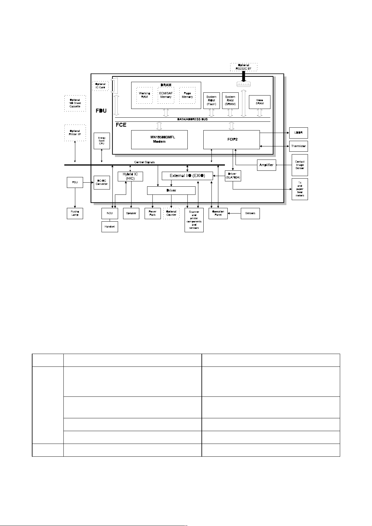
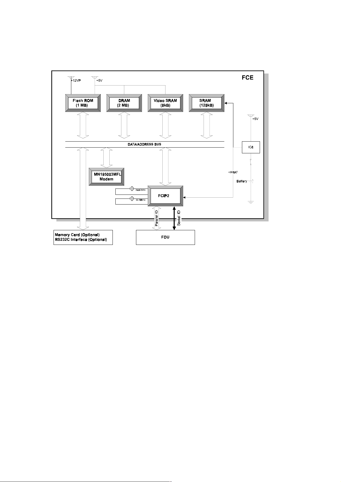
The FCE contains the FCIP2, DRAM, SRAM, System ROM, MN195003MFL modem, and
video processing memory. It controls the entire system through the FDU.
The FCIP2 does not contain the modem block. The Panasonic MN195003MFL modem is
used for all the communications (V.34, V.17, V.29, V.27ter., and V.21).
The 2 MB DRAM contains the SAF memory, ECM buffer memory, work area, and page
memory. The SAF memory can be extended by 1, 2 or 4 Mbytes with an IC card option.
A 1 MB (8 Mbit) flash ROM is used for the system ROM.
The FR6 uses two CPUs in the same way as the FX6. These are the main CPU in the
FCIP2 and the power saver CPU which is used during the 2 W power saver mode.
The main differences in PCB components between the FR6 and the FX6 are listed below.
FX6 FR6
FCIP used FCIP2 used
(The FCIP2 is used in common with
the LFO.)
FCE Rockwell R144EFXL modem used. Panasonic MN195003MFL modem
used.
512 kB (4 Mbit) flash ROM used. 1 MB (8 Mbit) flash ROM used.
1 MB DRAM used. 2 MB DRAM used.
FDU FPD motor driver used. SLA7024M motor driver used.
3
1.5. VIDEO DATA PATH
1.5.1 Transmission
TECHNICAL BULLETIN
Immediate Transmission:
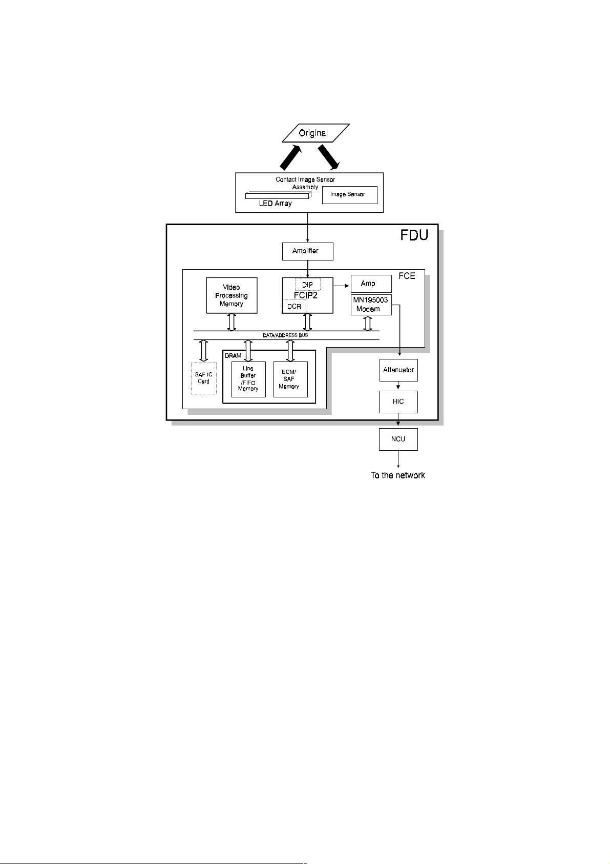
Scanned data from the CIS passes to the DIP block in the FCIP2. After analog/digital
video processing, the DCR block compresses the data for transmission. The compressed
data then passes either to the FIFO memory or to the ECM memory before it is sent
through the modem. The MN195003 modem is used for all the communications.
Memory Transmission:
The scanned data is stored in the SAF memory after compression in the DCR block.
At the time for transmission , the DCR block decompresses the data from the SAF
memory, then compresses it again after handshaking with the other terminal is done. The
compressed data then passes either to the FIFO memory or to the ECM memory, before it
is sent.
Parallel Memory Transmission:
This feature allows the machine to scan a document into the SAF memory and send the
same document simultaneously.
The machine stores the processed video data in the SAF memory and sends the data
through the modem at the same time.
4
1.5.2. Reception
TECHNICAL BULLETIN
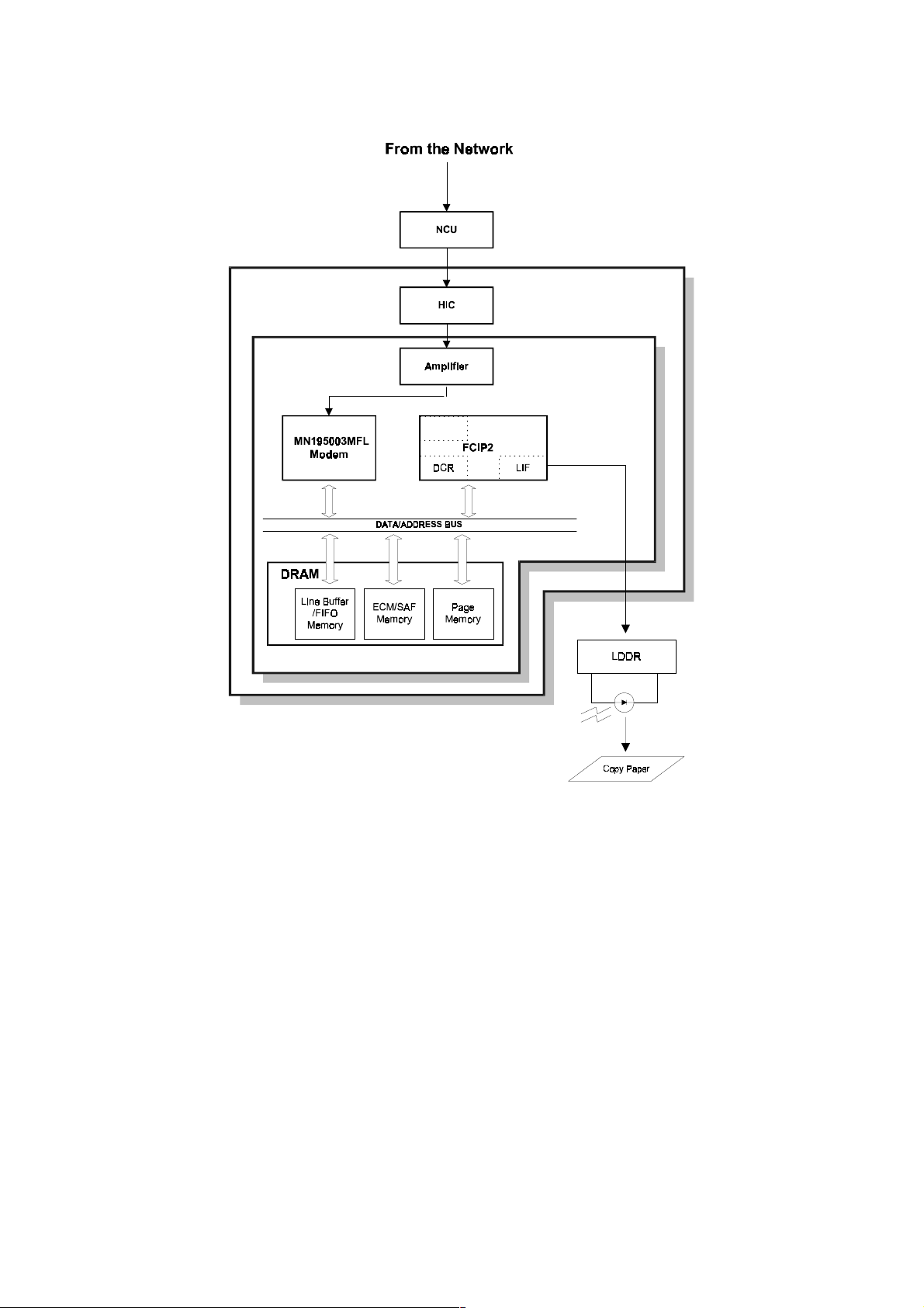
Data from the line passes to the modem through the NCU and hybrid IC. After the modem
demodulates the data, the decompressed data passes to the DCR block, through either
the FIFO or the ECM memory, where the data is decompressed to raster image data. At
the same time, the compressed data passes to the SAF memory as a backup in case of
mechanical problems during printing (substitute reception).
The raster image data is then passed to the page memory for printing. After a page of
data has been stored in the page memory, the data is sent to the LDDR through the LIF
block.
5
TECHNICAL BULLETIN
2. DETAILED SECTION DESCRIPTIONS
2.3. SYSTEM FEATURES
2.3.2. Automatic Service Calls
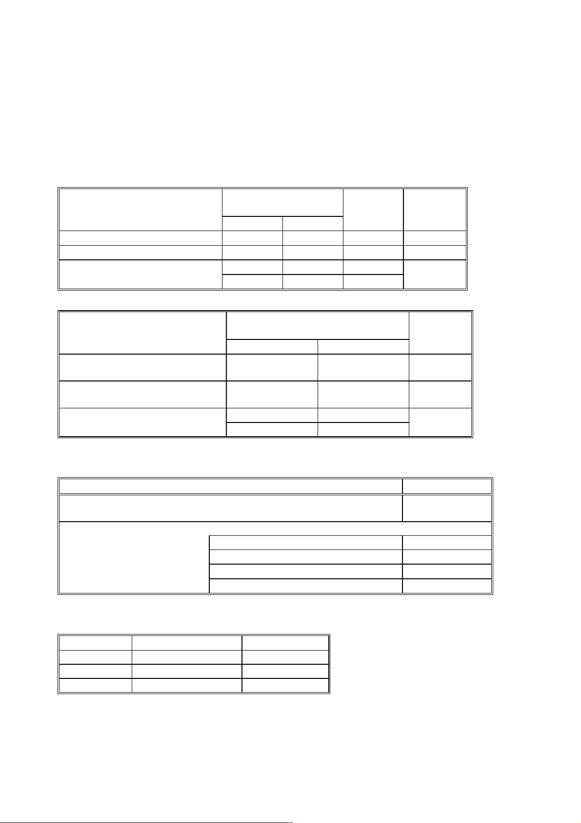
The following RAM addresses are different from the FX6.
2. Excessive Jam Alarms
Parameters Address (H) Initial
Settings
ADF Printer
DEC
(1 - 255; 0 = Disabled)
CALL
(3 - 15; 0 = Disabled)
CLR
Counters Address (H) Sys. Para.
JAM:
Jam counter used to place
a service call
NO-JAM1:
JAM counter decrement
NO-JAM2:
clearing the JAM counter 8001F0 (High) 8001F4 (High)
Counter used for
Counter used for
(Low)
(High)
8001F5 8001F9 10 (H) X
8001F6 8001FA 06 (H) Y
8001F7 8001FB 30 (H) –
8001F8 8001FC 00 (H)
ADF Printer
8001EE 8001F2 Z
8001ED 8001F1 –
8001EF (Low) 8001F3 (Low) –
3. Periodic Service Call
Sys. Para.
List
List
Parameters Address (H)
Call interval: 01 through 15 month(s) (BCD)
00: Periodic Service Call Disabled
Date and time of the next call
Year: last two digits of the year (BCD) 800267
Month: 01 through 12 (BCD) 800268
Day: 01 through 31 (BCD) 800269
Hour: 00 through 23 (BCD) 80026A
4. PM Call
Address (H) Bits 7 - 4 Bits 3 - 0
80019A Tens Units
80019B Thousands Hundreds
80019C Hundred thousands Ten thousands
800266
6

5. Effective Term of Service Calls
Year: last two digits of the year (BCD) 800271
Month: 01 through 12 (BCD) 800272
Day: 01 through 31 (BCD) 800273
TECHNICAL BULLETIN
Address (H)
7
2.4. PCBs
2.4.1. FCE
TECHNICAL BULLETIN
1. FCIP2 (Facsimile Controller and Image Processor)
• CPU
• Data compression and reconstruction (DCR)
• Digital image processor (DIP)
• Laser interface (LIF)
• DMA controller
• Clock generation
• Stepper motor control
• Serial interface to the FDU
• DRAM backup control
• Fusing lamp control
2. Modem (Panasonic MN195003MFL)
• V.34, V.17, V.29, V.27ter, V.21 modem
3. ROM
• 1 MB (8 Mbit) flash ROM for system software storage.
8

4. DRAM
• 2 MB DRAM shared between the Line Buffer (32 kB), ECM Buffer (128 kB), Page
Memory (768 kB), SAF memory (512 kB), and working area.
• Backed up by the battery on the FDU.
5. SRAM
• 128 kB SRAM for system and user parameter storage.
• Backed up by the battery on the FCE.
6. Video SRAM
• 8 kB SRAM for video processing.
7. Oscillators
• 29.952 MHz oscillator for system clock generation.
• 32.768 MHz oscillator for the real time clock. This is backed up by the battery on the
FCE.
• 24.192 MHz oscillator for the MN195003MFL modem.
TECHNICAL BULLETIN
8. Jumpers, Switches, and Test Points
Item Description
SW1 Switches the backup battery ON/OFF
9
2.4.2. FDU
TECHNICAL BULLETIN
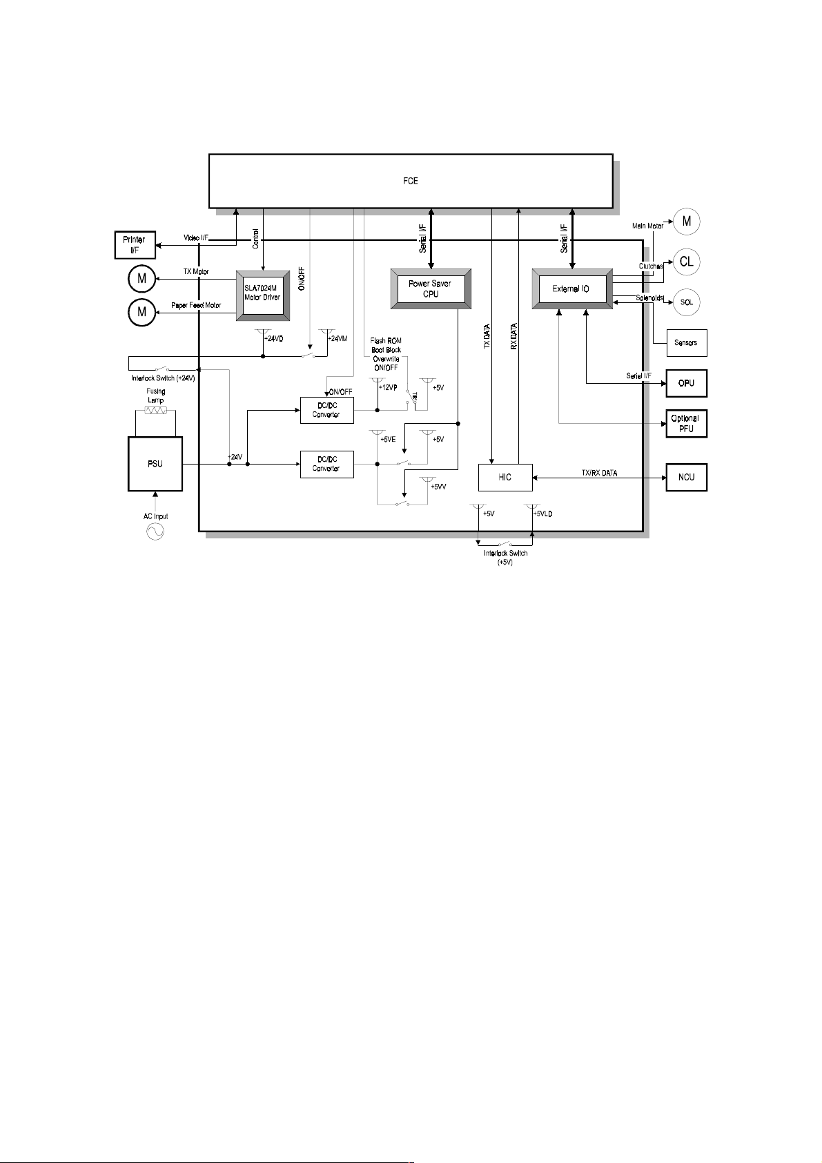
1. Power Saver CPU
• 4-bit CPU for controlling the machine during p ower saver mode
2. DC/DC Converters
• +5V generation
• +12V generation
3. Motor Driver (SLA7024M)
• Stepper motor driver
4. EXIO (External I/O)
• Serial interface to the FCE and OPU
• Serial interface to an optional paper feed unit
• Parallel interface to the main motor, clutches, and sensors
5. HIC (Hybrid IC)
• 2-4 wire switching
• Filters and amplifiers
• Monitor speaker driver
10
H516D531.CDR

6. Interlock Switches
• The fusing unit interlock switch (+24V) disables the power supply to the drive
components and the power pack.
• The fusing unit interlock switch (+5V) disables the laser diode power.
TECHNICAL BULLETIN
11
 Loading...