

Page 1
Model:
FR6
TECHNICAL BULLETIN
No:
Date:
31-Oct-97
001
1/35
Subject:
From:
New Model FR6 Release
Technical Service Department
Classification:
Troubleshooting
Mechanical
Paper path
Other ( )
Part information
Electrical
Transmit/receive
Prepared by:
Checked by:
Action required
Service manual revision
Retrofit information
K. Misugi
S. Fujii
The new model FR6 (FAX3800L) has been released as a successor model to the FX6
(FAX2700L).
This technical bulletin contains information on differences between the FR6 and the FX6.
They are listed in order of sections that appear in the service manual.
1. OVERALL MACHINE INFORMATION
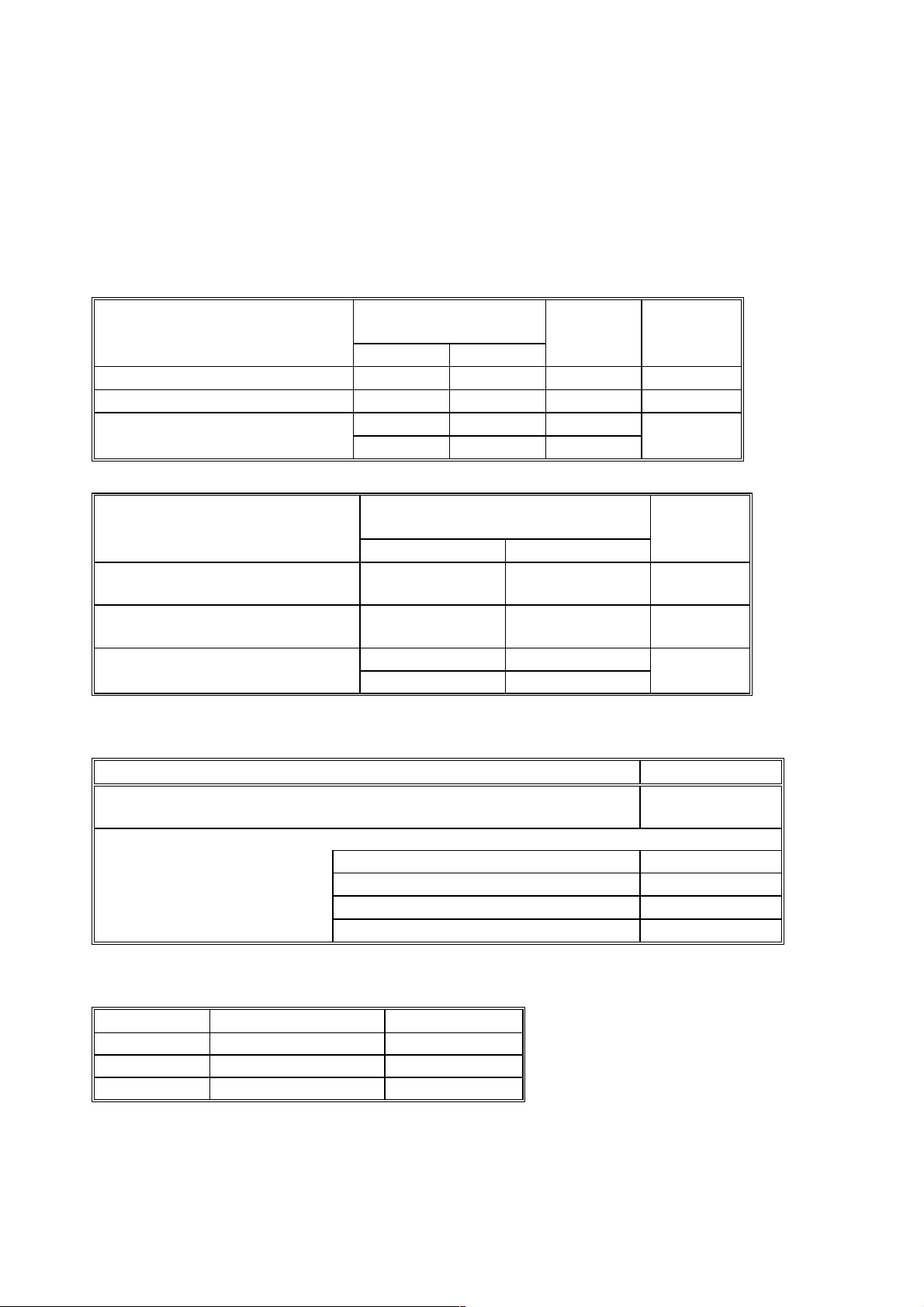
1.1. SPECIFICATIONS
Item FX6 FR6
Maximum Scan Width
216 mm [8.5 ins] ± 0.25% 256 mm [10 ins] ± 0.25%
(Effective Scan Width: 250 mm [9.8 ins])
Memory Capacity (SAF) 244 kbytes
(19 pages/ITU-T #1 Char t)
Compression MH, MR, EFC, MMR, SSC MH, MR, MMR, SS C
Modulation V.29, V.27, V.21 V.34, V.17, V.29, V.27ter, V.21
Data Rate 9,600/7,200/4,800/2,400 bps 33,600/31,200/28,800/26,400/
Transmission Time 9 s at 9600 bps; G3 ECM,
ITU-T # 1 Chart, STD
Paper Feed Unit Not Available Optional Paper Feed Unit Available (500
0.5 Mbyte
(40 pages/ITU-T #1 Char t)
With 1 Mbyte memory card:120 pages
With 2 Mbytes memory card: 200 pages
With 4 Mbytes memory card: 360 pages
24,000/21,600/19,200/16,800/
14,400/12,000/9,600/7,200/4, 800/
2,400 bps
Automatically adjusted in accordance
with V.34,
Automatic fallback t o V.17, V.29, V.27ter
3 s at 28,800 bps: G3 ECM, ITU-T # 1
Chart, STD
sheets, Letter, Legal)
1
Page 2

1.2. FEATURES
The following features are available.
Features FX6 FR6
Confidential Reception Available with memory card Standard
Batch Transmission Available with memory card Standard
Economy Transmission Not available Standard
Forwarding Available with memory card Standard
Personal codes with Conf. ID Available with memory card Standard
Transmission Deadline (TRD) Available with memory card Standard
Two in one Not available Available
Checkered mark Not available Available
Confidential ID Available with memory card Standard
Memory Lock (ID) Available with memory card Standard
Multi-Sort Document Reception Available with memory card Standard
TECHNICAL BULLETIN
Reverse Order Printing Available with memory card Standard
User Function Keys Not available Available (2 keys)
Confidential File Report Available with memory card Standard
2
Page 3
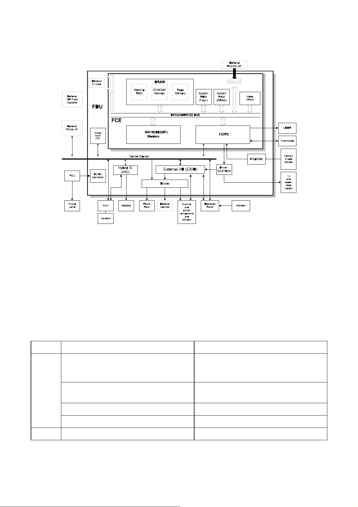
1.4. OVERALL MACHINE CONTROL
TECHNICAL BULLETIN
The FCE contains the FCIP2, DRAM, SRAM, System ROM, MN195003MFL modem, and
video processing memory. It controls the entire system through the FDU.
The FCIP2 does not contain the modem block. The Panasonic MN195003MFL modem is
used for all the communications (V.34, V.17, V.29, V.27ter., and V.21).
The 2 MB DRAM contains the SAF memory, ECM buffer memory, work area, and page
memory. The SAF memory can be extended by 1, 2 or 4 Mbytes with an IC card option.
A 1 MB (8 Mbit) flash ROM is used for the system ROM.
The FR6 uses two CPUs in the same way as the FX6. These are the main CPU in the
FCIP2 and the power saver CPU which is used during the 2 W power saver mode.
The main differences in PCB components between the FR6 and the FX6 are listed below.
FX6 FR6
FCIP used FCIP2 used
(The FCIP2 is used in common with
the LFO.)
FCE Rockwell R144EFXL modem used. Panasonic MN195003MFL modem
used.
512 kB (4 Mbit) flash ROM used. 1 MB (8 Mbit) flash ROM used.
1 MB DRAM used. 2 MB DRAM used.
FDU FPD motor driver used. SLA7024M motor driver used.
3
Page 4
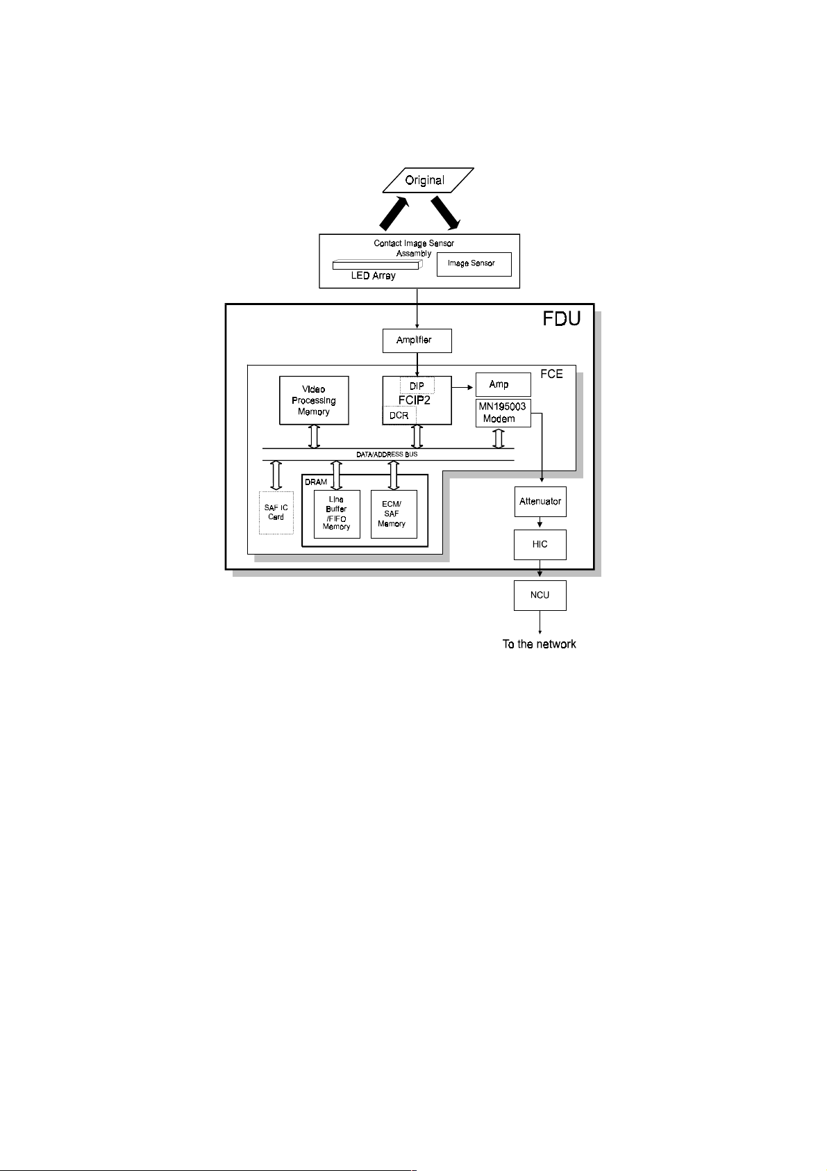
1.5. VIDEO DATA PATH
1.5.1 Transmission
TECHNICAL BULLETIN
Immediate Transmission:
Scanned data from the CIS passes to the DIP block in the FCIP2. After analog/digital
video processing, the DCR block compresses the data for transmission. The compressed
data then passes either to the FIFO memory or to the ECM memory before it is sent
through the modem. The MN195003 modem is used for all the communications.
Memory Transmission:
The scanned data is stored in the SAF memory after compression in the DCR block.
At the time for transmission , the DCR block decompresses the data from the SAF
memory, then compresses it again after handshaking with the other terminal is done. The
compressed data then passes either to the FIFO memory or to the ECM memory, before it
is sent.
Parallel Memory Transmission:
This feature allows the machine to scan a document into the SAF memory and send the
same document simultaneously.
The machine stores the processed video data in the SAF memory and sends the data
through the modem at the same time.
4
Page 5
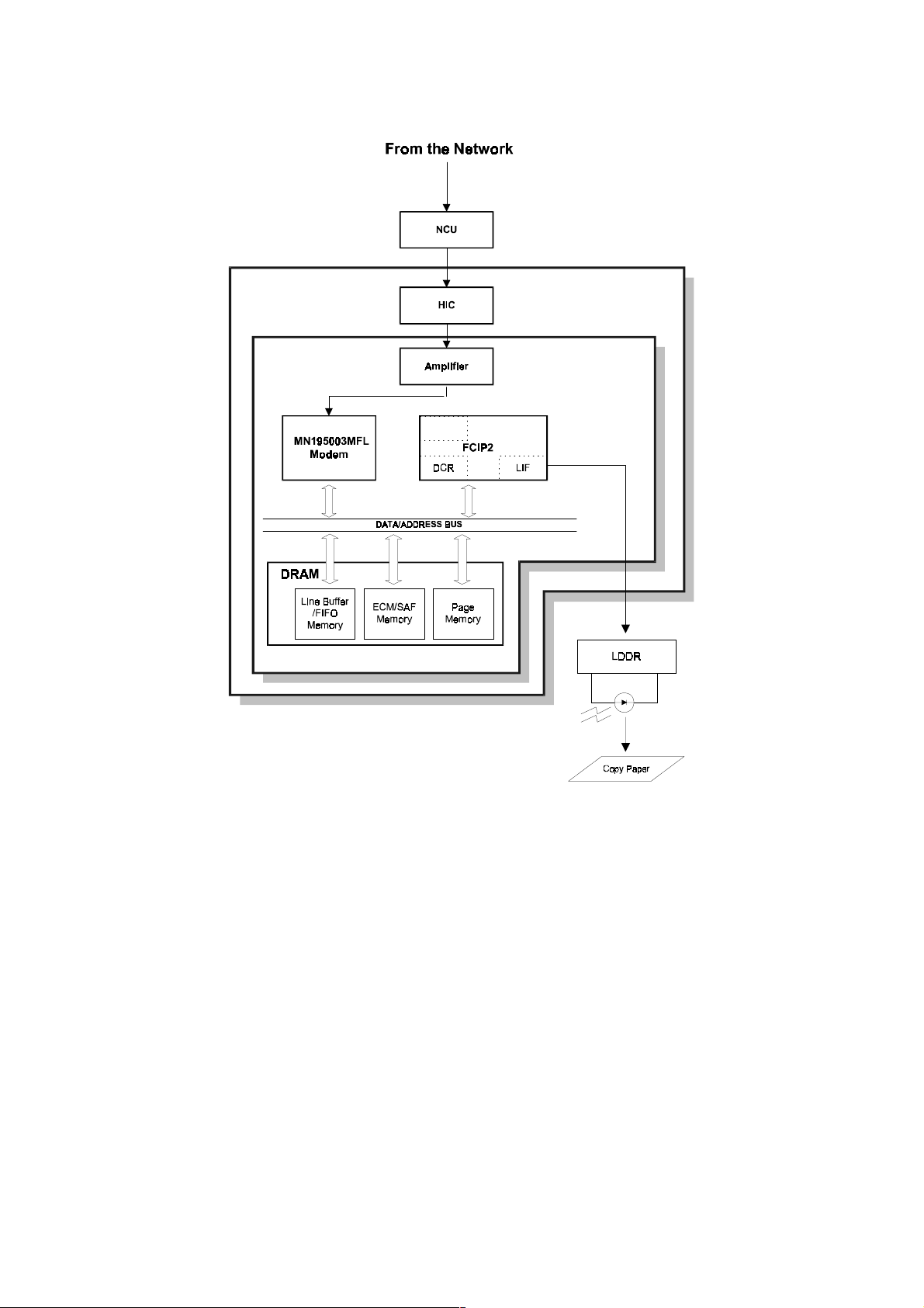
1.5.2. Reception
TECHNICAL BULLETIN
Data from the line passes to the modem through the NCU and hybrid IC. After the modem
demodulates the data, the decompressed data passes to the DCR block, through either
the FIFO or the ECM memory, where the data is decompressed to raster image data. At
the same time, the compressed data passes to the SAF memory as a backup in case of
mechanical problems during printing (substitute reception).
The raster image data is then passed to the page memory for printing. After a page of
data has been stored in the page memory, the data is sent to the LDDR through the LIF
block.
5
Page 6
TECHNICAL BULLETIN
2. DETAILED SECTION DESCRIPTIONS
2.3. SYSTEM FEATURES
2.3.2. Automatic Service Calls
The following RAM addresses are different from the FX6.
2. Excessive Jam Alarms
Parameters Address (H) Initial
Settings
ADF Printer
DEC
(1 - 255; 0 = Disabled)
CALL
(3 - 15; 0 = Disabled)
CLR
Counters Address (H) Sys. Para.
JAM:
Jam counter used to place
a service call
NO-JAM1:
JAM counter decrement
NO-JAM2:
clearing the JAM counter 8001F0 (High) 8001F4 (High)
Counter used for
Counter used for
(Low)
(High)
8001F5 8001F9 10 (H) X
8001F6 8001FA 06 (H) Y
8001F7 8001FB 30 (H) –
8001F8 8001FC 00 (H)
ADF Printer
8001EE 8001F2 Z
8001ED 8001F1 –
8001EF (Low) 8001F3 (Low) –
3. Periodic Service Call
Sys. Para.
List
List
Parameters Address (H)
Call interval: 01 through 15 month(s) (BCD)
00: Periodic Service Call Disabled
Date and time of the next call
Year: last two digits of the year (BCD) 800267
Month: 01 through 12 (BCD) 800268
Day: 01 through 31 (BCD) 800269
Hour: 00 through 23 (BCD) 80026A
4. PM Call
Address (H) Bits 7 - 4 Bits 3 - 0
80019A Tens Units
80019B Thousands Hundreds
80019C Hundred thousands Ten thousands
800266
6
Page 7

5. Effective Term of Service Calls
Year: last two digits of the year (BCD) 800271
Month: 01 through 12 (BCD) 800272
Day: 01 through 31 (BCD) 800273
TECHNICAL BULLETIN
Address (H)
7
Page 8
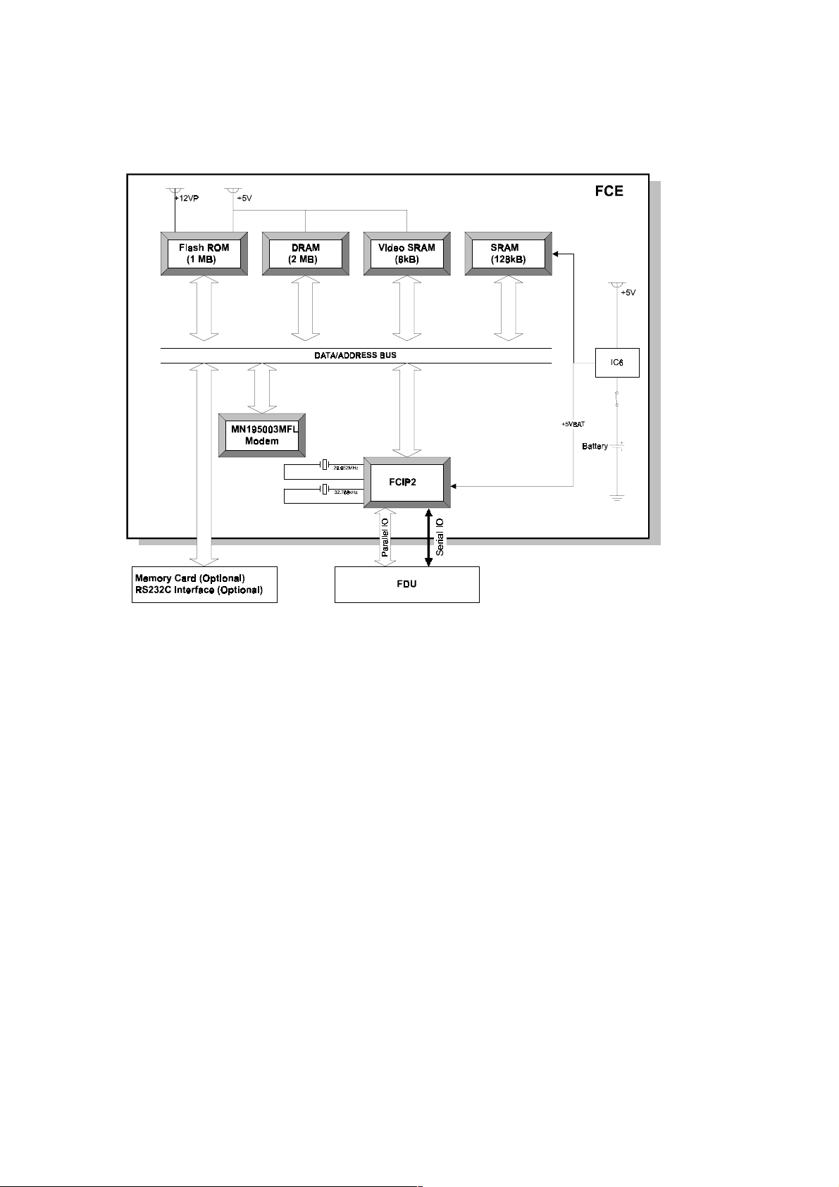
2.4. PCBs
2.4.1. FCE
TECHNICAL BULLETIN
1. FCIP2 (Facsimile Controller and Image Processor)
• CPU
• Data compression and reconstruction (DCR)
• Digital image processor (DIP)
• Laser interface (LIF)
• DMA controller
• Clock generation
• Stepper motor control
• Serial interface to the FDU
• DRAM backup control
• Fusing lamp control
2. Modem (Panasonic MN195003MFL)
• V.34, V.17, V.29, V.27ter, V.21 modem
3. ROM
• 1 MB (8 Mbit) flash ROM for system software storage.
8
Page 9

4. DRAM
• 2 MB DRAM shared between the Line Buffer (32 kB), ECM Buffer (128 kB), Page
Memory (768 kB), SAF memory (512 kB), and working area.
• Backed up by the battery on the FDU.
5. SRAM
• 128 kB SRAM for system and user parameter storage.
• Backed up by the battery on the FCE.
6. Video SRAM
• 8 kB SRAM for video processing.
7. Oscillators
• 29.952 MHz oscillator for system clock generation.
• 32.768 MHz oscillator for the real time clock. This is backed up by the battery on the
FCE.
• 24.192 MHz oscillator for the MN195003MFL modem.
TECHNICAL BULLETIN
8. Jumpers, Switches, and Test Points
Item Description
SW1 Switches the backup battery ON/OFF
9
Page 10
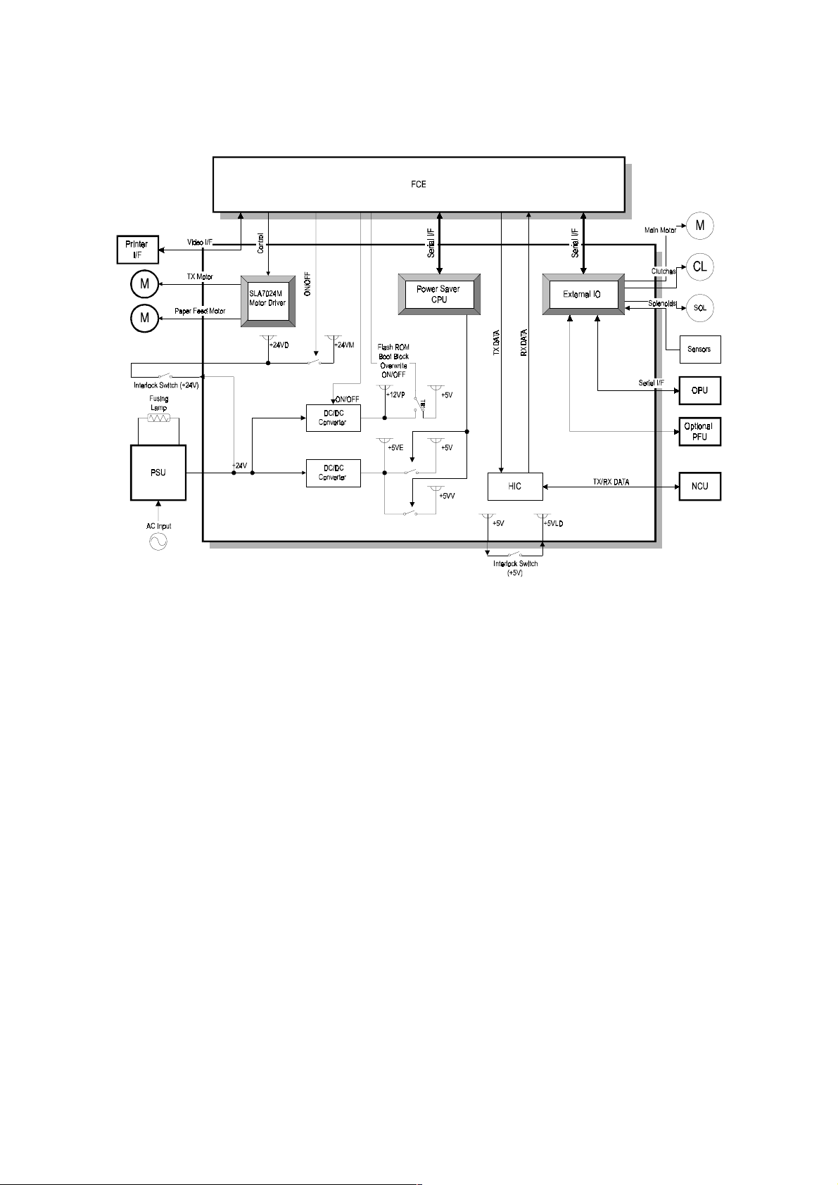
2.4.2. FDU
TECHNICAL BULLETIN
1. Power Saver CPU
• 4-bit CPU for controlling the machine during p ower saver mode
2. DC/DC Converters
• +5V generation
• +12V generation
3. Motor Driver (SLA7024M)
• Stepper motor driver
4. EXIO (External I/O)
• Serial interface to the FCE and OPU
• Serial interface to an optional paper feed unit
• Parallel interface to the main motor, clutches, and sensors
5. HIC (Hybrid IC)
• 2-4 wire switching
• Filters and amplifiers
• Monitor speaker driver
10
H516D531.CDR
Page 11

6. Interlock Switches
• The fusing unit interlock switch (+24V) disables the power supply to the drive
components and the power pack.
• The fusing unit interlock switch (+5V) disables the laser diode power.
TECHNICAL BULLETIN
11
Page 12
TECHNICAL BULLETIN
4. SERVICE TABLES AND PROCEDURES
4.1. SERVICE LEVEL FUNCTIONS
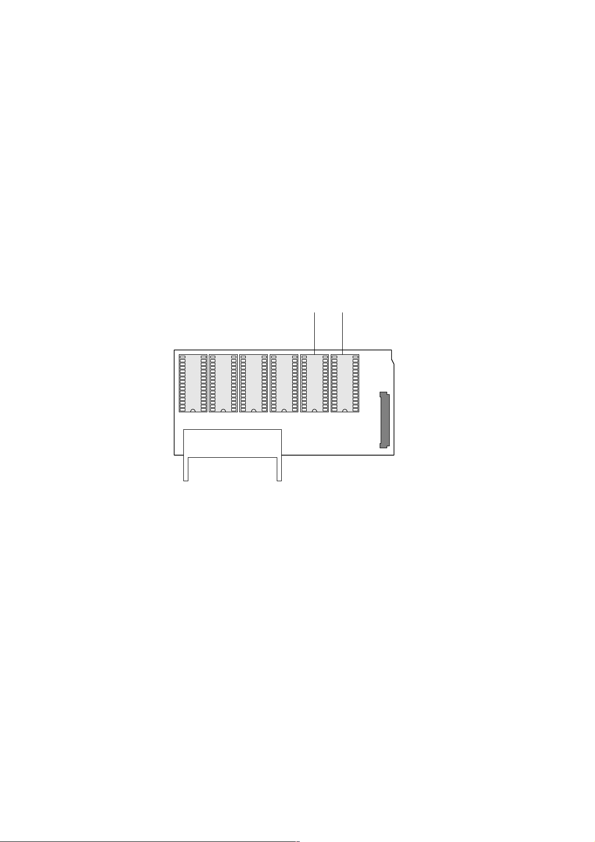
4.1.20. Software Download (Function 12)
This function copies software from an external medium to the Flash ROM on the
machine’s FCE. The procedures to download the software are the same as for the FX6
series.
However, if you are using the EPROM board, you must mount two 4-Mbit EPROMs
because this machine uses an 8-Mbit EPROM on the FCE.
NOTE:
The Flash/SRAM data copy board which is used in common with the ADAM and
LFO (P/N: A1939351) must be used for this procedure.
4M bit
(#1)
ROM BOARD II
4M bit
EPROM
(#2)
CN2
EPROM
(0H) U1 (1H) U2 (0L) U3 (1L) U4 U5 (L) U6 (H)
Data Copy Board P/N: A1939351
Mount the 4-Mbit EPROM #1 in the ROM socket U5 (L) and the 4-Mbit EPROM # 2 in the
ROM socket U6 (H) as shown.
It is not necessary to change the jumper at TB1 on the FCU or change system bit switch
02 bit 5 for this machine.
12
Page 13

4.2. BIT SWITCHES
RAM Reset Level 1:
The address for RAM reset level 1 has been changed to 800005(H).
Change the data to FF(H), then turn the machine off and on to reset all the system
settings.
Communication Parameters
Mode DCS: ITU-T standar d NSS: Non-standard G3
Modem rate 336: 33,600 bps 168: 16,800 bps
312: 31,200 bps 144: 14,400 bps
288: 28,800 bps 120: 12,000 bps
264: 26,400 bps 96: 9,600 bps
240: 24,000 bps 72: 7,200 bps
216: 21,600 bps 48: 4,800 bps
192: 19,200 bps 24: 2,400 bps
TECHNICAL BULLETIN
Communication mode ECM: Wit h ECM SSC: Using SSC
NML: With no ECM or SSC
Compression mode MMR: MMR compression
MR: MR compression
MH: MH compression
Resolution SSF: Fine, transm it t ed at 8 x 15.4 dot s per mm
DTL: Detail, transmitt ed at 8 x 7.7 dot s per mm
STD: Standard, transmit t ed at 8 x 3.85 dot s per mm
I/O rate 0M: 0 ms/line 10M: 10 ms/line
2/M: 2.5 ms/line 20M: 20 ms/line
5M: 5 ms/line 40M: 40 ms/line
Width and reduct ion =A4: A4 (8.3"), no reduction
=B4: B4 (10.1") no reduction
A4: Reduced to A4 (8.3") befor e transmission
System Switch 02
No FUNCTION COMMENTS
Not used Do not change the settings.
5
System Switch 06
No FUNCTION COMMENTS
PC Fax Expander Function
5
0: Disabled 1: Enabled
1: Set this bit to 1 when the PC Fax Expander option
has been installed.
13
Page 14

System Switch 10
No FUNCTION COMMENTS
Threshold memory level of
0
parallel memory transmission
to
7
System Switch 11
No FUNCTION COMMENTS
Conditions for memory
6
reception if no RTI or CSI is
received
0: Allow memory reception
only when RTI or CSI is
received
1: Allow memory reception
only when RTI or CSI is
received and a printer
(mechanical) error has
occurred
TECHNICAL BULLETIN
Threshold memory = N × 64 kbytes + 256 kbytes
N can be between 00 - FF(H)
Default setting: 04(H) = 512 kbyte
This switch functions in combination with user
parameter switch 05 bit 1.
User parameter switch 05 bit 1 must be set to 1 t o
enable this switch.
User parameter switch 05 bit 1:
Switch to allow memory reception if no RTI or CSI is
received.
0: Allow memory reception for all comm unications
1: Reject if RTI or CSI is not received
System Switch 17
No FUNCTION COMMENTS
Dialing without inserting a
6
document
0: Disabled
1: Enabled
Printer Switch 02
No FUNCTION COMMENTS
Paper Feed Priority
0
0:
Optional paper feed unit >>
100-sheet cassette >>
Standard cassette
1:
Optional paper feed unit >>
Standard cassette >> 100sheet cassette
Communication Swit ch 01
No FUNCTION COMMENTS
Not used Do not change the settings.
1
0: Dialing cannot be done without inserting a
document in the ADF.
This bit determines which set of priorities t he
machine uses for feeding t he paper when all the
cassettes contain the same paper size.
14
Page 15

Communication Swit ch 17
No FUNCTION COMMENTS
Selective Polling Reception
0
0: Disabled
1: Enabled
Subaddress function (RX)
1
0: Disabled
1: Enabled
G3 Switch 03
No FUNCTION COMMENTS
Use of V.8 protocol
2
0: Disabled
1: Enabled
TECHNICAL BULLETIN
1: Selective polling reception (SEP) is disabled.
1: Subaddress reception is disabled.
1: V.8 protocol is disabled.
15
Page 16

G3 Switch 05
FUNCTION COMMENTS
Initial Tx modem rat e
0
Bit 3 2 1 0 Setting (bps)
to
0 0 0 1 2.4k
3
0 0 1 0 4.8k
0 0 1 1 7.2k
0 1 0 0 9.6k
0 1 0 1 12.0k
0 1 1 0 14.4k
0 1 1 1 16.8k
1 0 0 0 19.2k
1 0 0 1 21.6k
1 0 1 0 24.0k
1 0 1 1 26.4k
1 1 0 0 28.8k
1 1 0 1 31.2k
1 1 1 0 33.6k
Other settings - Not used
Initial modem type for 9. 6k or
4
7.2kbps (transmission)
to
Bit 5 Bit 4 Setting
5
0 0 V.29
0 1 V.17
1 0 Not used
1 1 Not used
TECHNICAL BULLETIN
These bits set the initial start ing m odem rate for
transmission.
Use the dedicated transmission parameters if you
need to change this for specif ic receivers.
These bits set the initial modem t ype for 9.6k and
7.2kbps, if the init ial modem rate is set at these
speeds.
G3 Switch 06
FUNCTION COMMENTS
Initial Rx modem rate
0
Bit 3 2 1 0 Setting (bps)
to
0 0 0 1 2.4k
3
0 0 1 0 4.8k
0 0 1 1 7.2k
0 1 0 0 9.6k
0 1 0 1 12.0k
0 1 1 0 14.4k
0 1 1 1 16.8k
1 0 0 0 19.2k
1 0 0 1 21.6k
1 0 1 0 24.0k
1 0 1 1 26.4k
1 1 0 0 28.8k
1 1 0 1 31.2k
1 1 1 0 33.6k
Other settings - Not used
The setting of these bit s is used t o inform the
transmitting terminal of the available modem rate for
the machine in receive mode.
Use a lower setting if high speeds pose problems
during reception.
16
Page 17

TECHNICAL BULLETIN
Modem types available for
4
reception
to
Bit 7 6 5 4 Setting
7
0 0 0 1 V.27ter
0 0 1 0 V.27ter, V.29
0 0 1 1 Not used
0 1 0 0 V.27ter, V.29,
V.17,
0 1 0 1 V.27ter, V.29,
V.17, V.34
Other settings - Not used
The setting of these bit s is used t o inform the
transmitting terminal of the available modem type for
the machine in receive mode.
17
Page 18

4.5. SERVICE RAM ADDRESSES
The complete RAM addresses are listed because there are too many changes from the
FX6.
800005(H) - RAM Reset Level 1
Change the data at this address to FF (H), then switch the machine off and on to reset all
the system settings.
Caution:
Parameter List).
800001 to 800004(H) - ROM version (Read only)
800001(H) - Revision number (BCD)
800002(H) - Year (BCD)
800003(H) - Month (BCD)
800004(H) - Day (BCD)
Before using this RAM, print the settings of all the system parameters (System
TECHNICAL BULLETIN
800006 to 800016(H)
800018(H)
800019(H)
80001A(H)
80001B(H)
80001C(H)
80001D(H)
80001E(H)
800020 to 80003F(H)
800040 to 80004F(H)
800050 to 80005F(H)
800060 to 80007F(H)
800080 to 80008F(H)
8000A0(H) - User parameter switch 00
Bit 0: Stamp home position 0: Disabled, 1: Enabled
Bits 1 and 2: Scanning contrast home position
Bit 2 1 Setting
0 0 Normal
0 1 Lighten
1 0 Darken
Bit 3: Do not adjust
Bits 4 and 5: Scanning resolution home position
Bit 5 4 Setting
0 0 Standard
0 1 Detail
1 0 Fine
Bit 6: Transmission mode home position 0: Memory tx, 1: Immediate tx
Bit 7: Halftone home position 0: Disabled, 1: Enabled
- Total program checksum (low)
- Total program checksum (high)
- Boot program checksum (low)
- Boot program checksum (high)
- Main program checksum (low)
- Main program checksum (high)
- RDS program update counter (hex)
- Machine's serial number (17 digits - ASCII)
- System bit switches
- Scanner bit switches
- Printer bit switches
- Communication bit switches
- G3 bit switches
18
Page 19

8000A1(H) - User parameter switch 01
Bits 0 to 6: Not used
Bit 7: Settings return to home position after transmission 0: Disabled , 1: Enabled
8000A2(H) - User parameter switch 02
Bit 0: Forwarding mark printing on forwarded messages 0: Disabled, 1: Enabled
Bit 1: Center mark printing on received copies 0: Disabled, 1: Enabled
Bit 2: Reception time printing 0: Disabled, 1: Enabled
Bit 3: TSI included in transmitted messages 0: Disabled, 1: Enabled
Bit 4: Checkered mark printing 0: Disabled, 1: Enabled
Bits 5 to 7: Not used
TECHNICAL BULLETIN
8000A3(H) - User parameter switch 03
Bit 0: Transmission result report (memory transmissions) 0: Off, 1: On
Bit 1: Not used
Bit 2: Memory storage report 0: Off, 1: On
Bit 3: Polling reserve report (polling reception) 0: Off, 1: On
Bit 4: Polling result report (polling reception) 0: Off, 1: On
Bit 5: Transmission result report (immediate transmissions) 0: Off, 1: On
Bit 6: Polling clear report 0: Off, 1: On
Bit 7: TCR (Journal) 0: Off, 1: On
8000A4(H) - User parameter switch 04
Bit 0: Automatic confidential reception report output 0: Off, 1: On
Bits 1 to 6: Not used
Bit 7: Inclusion of a sample image on reports 0: Off, 1: On
8000A5(H) - User parameter switch 05
Bit 0: Substitute reception 0: Off, 1: On
Bit 1: Memory reception if no RTI or CSI received 0: Possible, 1: Impossible
Bits 2 and 3: Not used
Bit 4: Restricted Access 0: Off, 1: On
Bit 5: Not used (keep this bit at 0.)
Bit 6: Fusing lamp control during energy saver mode
0: Lamp off, 1: Standby temperature (80 °C)
Bit 7: Not used (keep this bit at 0.)
(Automatic report printout)
8000A6(H) - User parameter switch 06
Bit 0: TTI 0: Off, 1: On
Bit 1: Not used
Bit 2: Closed network for transmission 0: Off, 1: On
Bit 3: Not used
Bit 4: Batch transmission 0: Off, 1: On
Bits 5 to 7: Not used
19
Page 20

8000A7(H) - User parameter switch 07
Bits 0 to 2: Not used
Bit 3: Automatic reduction (B4 ->> A4) before transmission 0: Off, 1: On
Bits 4 to 7: Not used
8000A8(H) - User parameter switch 08
Bit 0 and 1: Multi-copy reception
Bit 1 0 Setting
X 0 Disabled
0 1 Faxes from senders whose RTIs/CSIs are specified for this
feature are multi-copied.
1 1 Faxes from senders whose RTIs/CSIs are not specified for
this feature are multicopied.
Bits 2 and 3: Authorized reception
Bit 3 2 Setting
X 0 Disabled
0 1 Faxes from senders whose RTIs/CSIs are specified for this
feature are accepted.
1 1 Faxes from senders whose RTIs/CSIs are not specified for
this feature are accepted.
Bits 4 and 5: Specified cassette selection (optional PFU required)
Bit 3 2 Setting
X 0 Disabled
0 1 Faxes from senders whose RTIs/CSIs are specified for this
feature are printed to the paper in a specified cassette.
1 1 Faxes from senders whose RTIs/CSIs are not specified for
this feature are printed to the paper in a specified cassette.
Bits 6 and 7: Forwarding
Bit 1 0 Setting
X 0 Disabled
0 1 Faxes from senders whose RTIs/CSIs are specified for this
feature are forwarded.
1 1 Faxes from senders whose RTIs/CSIs are not specified for
this feature are forwarded.
TECHNICAL BULLETIN
8000A9(H) - User parameter switch 09
Bits 0 and 1: Memory lock (optional memory card required)
Bit 1 0 Setting
X 0 Disabled
0 1 Faxes from senders whose RTIs/CSIs are specified are kept
in the memory until a memory lock ID is entered.
1 1 Faxes from senders whose RTIs/CSIs are not specified are
kept in the memory until a memory lock ID is entered.
Bits 2 to 7: Not used
20
Page 21

8000AA(H) - User parameter switch 10
Bit 0: Reverse order printing 0: Disabled, 1: Enabled
Bit 1: Two in 1 (printing two Half-letter (A5) messages onto one Letter (A4) paper)
Bits 2 to 6: Not used
Bit 7: Halftone type 0: Error diffusion, 1: Dither
8000AB(H) - User parameter switch 11
Bits 0 to 5: Not used
Bit 6: Printout of messages received while acting as a forwarding station
Bit 7: Polling Standby duration 0: Once, 1: No limit
8000AC(H) - User parameter switch 12
Bits 0 and 1: Not used
Bit 2: Toner saving mode 0: Disabled, 1: Enabled
Bits 3 and 4: Printout image density (Fax mode)
Bit 4 3 Setting
0 0 Normal
0 1 Lighten
1 0 Darken
1 1 Not used
Bits 5 to 7: Not used
TECHNICAL BULLETIN
0: Disabled, 1: Enabled
0: Off, 1: On
8000AD(H) - User parameter switch 13
Bits 0 and 1: PSTN access method from behind PABX
Bit 1 0 Setting
0 0 PSTN
0 1 Loop start
1 0 Ground start
1 1 Flash start
Bits 2 to 7: Not used
8000AE - 8000AF(H) - User parameter 14 to 15
Not used
8000B9(H) - User function 62 settings
Bit 0: Night timer 0: Disabled, 1: Enabled
Bits 1 to 3: Not used
Bit 4: RDS operation 0: Not acceptable
1: Acceptable for the limit specified by system switch 03
Bits 5 and 6: Not used
Bit 7: Daylight saving time 0: Disabled, 1: Enabled
8000BA(H) - User function 62 settings
Bit 0: Not used
Bit 1: Dialing type 0: Pulse dialing (10 pps), 1: Tone (DTMF) dialing
Bits 2 to 7: Not used
21
Page 22

8000BB(H) - PSTN access number for loop start
Access number Hex value to program (BCD)
0 F0
ØØ
0 F0
00 00
ØØ
99 99
8000C8 to 8000DB(H) - RTI (Max. 20 characters - ASCII) - Note 1
8000DC to 8000EF(H) - CSI (Max. 20 characters - ASCII)
8000F0 to 80010F(H) - TTI (Max. 32 characters - ASCII) - Note 1
800110(H) - Number of CSI characters (Hex)
Note 1: If the number of characters are less than the maximum (20 for RTI, 32 for TTI),
add a stop code (FF[H]) after the last character.
800111 to 80011F(H) - Service station's fax number (Service function 13)
800120 to 80012E(H) - Own fax number (User function 61)
80012F(H) - ID code (low - Hex)
800130(H) - ID code (high - Hex)
TECHNICAL BULLETIN
800131(H) - Confidential ID (low - BCD)
800132(H) - Confidential ID (high - BCD)
800133(H) - Memory lock ID (low - Hex)
800134(H) - Memory lock ID (high - Hex)
800140 to 800146(H) - Last power off time (Read only)
800140(H) - Year (BCD)
800141(H) - Month (BCD)
800142(H) - Day (BCD)
800143(H) - 00: Monday, 01: Tuesday, 02: Wednesday, ....... , 06: Sunday
800144(H) - Hour
800145(H) - Minute
800146(H) - Second
800150(H) - Optional equipment (Read only)
Bit 0: Memory card 0: Not installed, 1: Installed
Bit 1-3: Not used
Bit 4: 100-sheet cassette 0: Not installed, 1: Installed
Bit 5: Paper feed unit 0: Not installed, 1: Installed
Bit 6-7: Not used
800151(H) - Optional equipment (Read only)
Bit 0: Not used
Bit 1: Printer interface 0: Not installed, 1: Installed
Bit 2-7: Not used.
22
Page 23

The following counters are listed on the System Parameter List. The names used on the
system parameter list are given in brackets
TECHNICAL BULLETIN
800158 to 80015A(H)
Address High Low
800158(H) Tens digit Unit digit
800159(H) Thousands digit Hundreds digit
80015A(H) Millions digit Ten thousands digit
Note:
80015B to 80015D(H)
80015E to 800160(H)
800161 to 800163(H)
800164 to 800166(H)
800167 to 800169(H)
80016A to 80016C(H)
80016D to 80016F(H)
800170 to 800172(H)
800176 to 800178(H)
The following counters have the same data format as above.
- Tx counter (TX)
- Rx counter (RX)
- Scan counter (SCN)
- Print counter (PRT)
- Printer interface output counter (PRN)
- Paper feed counter: standard cassette (UPPER CASSETTE)
- Paper feed counter: optional PFU (CASSETTE 2)
- Paper feed counter: optional 100-sheet cassette
- Paper feed counter: bypass feed (BY-PASS)
- ADF counter (ADF)
80017C to 80017E(H)
80017F to 800181(H)
800182 to 800184(H)
800185 to 800187(H)
800188 to 80018A(H)
80018B to 80018D(H)
80018E to 800190(H)
800191 to 800193(H)
800197 to 800199(H)
80019A to 80019C(H)
80019D to 80019F(H)
8001A0 to 8001A2(H)
8001A3 to 8001A5(H)
The machine asks the user to replace the drum at this interval, if bit 3 of system bit switch
04 is 0.
8001A6 to 8001A8(H)
- Printer total jam counter (COPY JAM)
- Paper jam counter: standard cassette (UPPER CST JAM)
- Paper jam counter: optional PFU (CST 2 JAM)
- Paper jam counter: optional 100-sheet cassette (OPEN CST JAM)
- Paper jam counter: bypass feed (BY-PASS)
- Scanner total jam counter (DOC. JAM)
- Fusing exit jam counter (EJECT JAM)
- Registration jam counter (PAPER JAM)
- PM counter (PM)
- PM call interval: default 60,000 (PM DEFAULT)
- Copy counter (COPY)
- OPC (master drum) counter (PCU)
- OPC (master drum) replacement interval (default: 30,000 prints)
- CTM counter (TONER)
8001ED to 8001FC(H)
800200(H)
- Number of copies in multi-sort document reception (User function 83)
- Excessive jam call parameters
23
Page 24

800201 to 80022A(H) - Night timer period (User function 71)
800201 to 800203(H) - Setting #1 for Monday
800204 to 800206(H) - Setting #2 for Monday
800207 to 800209(H) - Setting #1 for Tuesday
80020A to 80020C(H) - Setting #2 for Tuesday
80020D to 80020F(H) - Setting #1 for Wednesday
800210 to 800212(H) - Setting #2 for Wednesday
800213 to 800215(H) - Setting #1 for Thursday
800216 to 800218(H) - Setting #2 for Thursday
800219 to 80021B(H) - Setting #1 for Friday
80021C to 80021E(H) - Setting #2 for Friday
80021F to 800221(H) - Setting #1 for Saturday
800222 to 800224(H) - Setting #2 for Saturday
800225 to 800227(H) - Setting #1 for Sunday
800228 to 80022A(H) - Setting #2 for Sunday
Program format
First byte - Hour (BCD)
Second byte - Minute (BCD)
Third byte - 00(H): Timer start time, 01(H): Timer end time
TECHNICAL BULLETIN
800255 to 80025B(H) - Last RDS operation (Read only)
800255(H) - Year (BCD)
800256(H) - Month (BCD)
800257(H) - Day (BCD)
800258(H) - 00: Monday, 01: Tuesday, 02: Wednesday, ....... , 06: Sunday
800259(H) - Hour
80025A(H) - Minute
80025B(H) - Second
80025D(H)
800260(H)
800261(H)
800262(H)
800264(H)
800265(H)
800266 to 80026A(H)
800271 to 800273(H)
8002B4 to 8002B5(H)
8002B6 to 8002B7 (H)
- Daylight saving time setting (User function 62)
- Transmission monitor volume 00 - 07(H)
- Reception monitor volume 00 - 07(H)
- On-hook monitor volume 00 - 07(H)
- Buzzer volume 00 - 07(H)
- Key acknowledgment tone volume00 - 07(H)
- Periodic service call parameters
- Effective term of automatic service calls
- Scanning top margin adjustment
- Scanning bottom margin adjustment
24
Page 25

80036F(H) - Details of the service call (hardware error)
01(H) - The fusing lamp temperature stayed above 175 °C while printing.
02(H) - The fusing lamp temperature did not reach 150 °C before starting printing.
03(H) - The fusing lamp temperature did not go down to 100 °C while in standby mode
(when fusing lamp OFF was selected for power saver mode)
04(H) - The fusing lamp temperature did not go down to 100 °C while in standby mode
(when fusing lamp Standby (100 °C) was selected for power saver mode)
05(H) - The fusing lamp temperature stayed below 100 °C while in standby mode (when
fusing lamp Standby (100 °C) was selected for power saver mode)
07(H) - The fusing lamp temperature came below 140 °C while printing
08(H) - The fusing lamp temperature exceeded 250 °C
09(H) - A fusing thermistor error was detected
TECHNICAL BULLETIN
NOTE:
800370(H) - Excessive jam alarm
Bit 3: Scanner excessive jam alarm 1: An alarm has occurred
Bit 4: Printer excessive jam alarm 1: An alarm has occurred
NOTE:
800371(H) - Details of the service call (hardware error)
01(H) - The fusing lamp temperature stayed above 175 °C while printing.
02(H) - The fusing lamp temperature did not reach 150 °C before starting printing.
03(H) - The fusing lamp temperature did not go down to 100 °C while in standby mode
(when fusing lamp OFF was selected for power saver mode)
04(H) - The fusing lamp temperature did not go down to 100 °C while in standby mode
(when fusing lamp Standby (100 °C) was selected for power saver mode)
05(H) - The fusing lamp temperature stayed below 100 °C while in standby mode (when
fusing lamp Standby (100 °C) was selected for power saver mode)
07(H) - The fusing lamp temperature came below 140 °C while printing
08(H) - The fusing lamp temperature exceeded 250 °C
09(H) - A fusing thermistor error was detected
11(H) - Charge leak current was detected while the charge corona unit was activated
12(H) - Charge leak current was detected while the charge corona unit was not activated
21(H) - The laser synchronization signal was not detected during printing
31(H) - Polygonal mirror motor startup error
32(H) - Polygonal mirror motor error during printing
41(H) - Main motor startup error
42(H) - Main motor erro r during printing
When a service call was caused by a fusing unit failure (codes 01 - 09):
After fixing the problem, reset the data at this address to 00(H), then restart the
machine to clear the service call. (Refer to address 800371(H) for other hardware
failures.)
Either or both of these bits will change to 1 when an excessive jam alarm occurs.
Reset each bit to 0 when you have solved the problem. The machine will not be
able to detect excessive jams in future if you do not reset these bits.
25
Page 26

TECHNICAL BULLETIN
NOTE:
800383(H)
800384(H)
800385(H)
800386(H)
800388(H)
800389(H)
80038A(H)
80038B(H)
80039D(H)
Bit 0 to 3: Paper size sensor
Bit 3 2 1 0 Setting
0 0 0 1 Cassette not installed
0 0 1 0 Cassette not installed
0 1 0 0 Letter
0 1 0 1 Cassette not installed
0 1 1 0 Cassette not installed
0 1 1 1 Legal
1 0 0 0 Cassette not installed
Bit 4: Paper end sensor 1: Paper end
Bit 5: Registration sensor 1: Paper present
Bit 6: Fusing exit sensor 1: Paper present
Bit 7: Standard cassette availability 0: Available, 1: Not available
When a service call was caused by a fusing lamp failure (codes 01 - 09):
The same code is stored at address 80036F(H).
After fixing the problem, reset the data at address 80036F(H) to 00(H), then
restart the machine to clear the service call.
When a service call was caused by another hardware failure (codes 11 - 42):
If the problem remains after restarting the machine (power off/on), fix the
hardware problem. The service call condition is cleared after power-up.
- Print top margin (standard cassette)
- Print top margin (optional PFU)
- Print top margin (optional 100-sheet cassette)
- Print top margin (bypass feeder)
- Print left margin (standard cassette)
- Print left margin (optional PFU)
- Print left margin (optional 100-sheet cassette)
- Print left margin (bypass feeder)
- Sensor status (standard cassette and internal printer mechanism)
(1: Jam, paper end, etc.)
80039E(H)
Bit 0 to 3: Paper size sensor - The settings are the same as the standard cassette.
Bit 4: Paper end sensor 1: Paper end
Bit 5: Registration sensor 1: Paper present
Bit 6: Not used
Bit 7: Cassette availability 0: Available, 1: Not available
- Sensor status (optional PFU)
(1: Jam, paper end, etc.)
26
Page 27

TECHNICAL BULLETIN
80039F(H)
Bit 0 to 3: Paper size sensor - The settings are the same as the standard cassette.
Bit 4: Paper end sensor 1: Paper end
Bit 5: Not used
Bit 6: Not used
Bit 7: Standard cassette availability 0: Available, 1: Not available
8003A0(H)
Bit 0 to 3: Not used
Bit 4: Paper in the bypass feed 1: Paper not present
Bit 5: Bypass feed sensor 1: Paper present
Bit 6: Not used
Bit 7: Bypass feed availability 0: Available, 1: Not available
8003AA(H)
Bit 3: Initial toner supply 0: Off, 1: On
Whenever the development unit is replaced, do the following procedure.
1. Make sure that a new development unit, drum, and CTM are correctly installed.
2. Turn on the machine and change this bit to 1.
3. Turn off the machine.
4. Turn on the machine. The machine starts filling up the empty development unit hopper
with new toner. (This bit is reset to zero automatically.)
5. Make test copies or test patterns to check the print quality.
- Sensor status (optional 100-sheet cassette)
(1: Jam, paper end, etc.)
- Sensor status (bypass feed)
(1: Jam, no paper, etc.)
- Initial Toner Supply
803540 to 8036BF(H) - Latest 64 error codes (Read only)
One error record consists of 6 bytes of data.
First error record start address - 803540(H)
Second error record start address - 803546(H)
Third error record start address - 80355C(H)
: : :
64th error record start address - 8036BA(H)
The format is as follows:
1st byte - Minute (BCD)
2nd byte - Hour (BCD)
3rd byte - Day (BCD)
4th byte - Month (BCD)
5th byte - Error code (low) [If the error code is 1-23, 23 is stored here.]
6th byte - Error code (high) [If the error code is 1-23, 01 is stored here.]
27
Page 28

803D46 to 803F57(H) - Latest 10 error communication records
One error communication record consists of 53 bytes. The format is as follows:
1st byte - Header
Bit 0: Communication result 0: OK, 1: NG
Bit 1: Document jam 1: Occurred
Bits 2 - 3: Not used
Bit 4: Technical data printout instead of personal codes 0: No, 1: Yes
Bit 5: Type of technical data 0: Rx level, 1: Measure of error rate
Bit 6: Error report 0: Not printed, 1: Printed
Bit 7: Data validity 0: Not valid, 1: Valid
2nd to 5th bytes - Date and time when the communication started
2nd byte - Month (BCD)
3rd byte - Day (BCD)
4th byte - Hour (BCD)
5th byte - Minute (BCD)
6th and 7th bytes - Communication time
6th byte - Minutes (BCD)
7th byte - Seconds (BCD)
TECHNICAL BULLETIN
8th byte - Number of pages transmitted or received (Hex)
9th and 10th bytes - Personal code or number of total/burst error lines
If bit 4 of the 1st byte is 0:
9th byte - Personal code (low - BCD)
10th byte - Personal code (high - BCD)
If bit 4 of the 1st byte is 1:
9th byte - Number of total error lines (Hex)
10th byte - Number of burst error lines (Hex)
11th byte - File number (low - Hex)
12th byte - File number (high - Hex)
13th and 14th bytes - Rx level or measure of error rate
If bit 5 of the 1st byte is 0:
13th byte - Rx level (low - Hex)
14th byte - Rx level (high - Hex)
If bit 4 of the 1st byte is 1:
13th byte - Measure of error rate (low - Hex)
14th byte - Measure of error rate (high - Hex)
28
Page 29

15th byte - Final modem rate
Bits 0 to 3: Final modem speed
Bit 3 2 1 0 Setting (bps)
0 0 0 1 2.4k
0 0 1 0 4.8k
0 0 1 1 7.2k
0 1 0 0 9.6k
0 1 0 1 12.0k
0 1 1 0 14.4k
0 1 1 1 16.8k
1 0 0 0 19.2k
1 0 0 1 21.6k
1 0 1 0 24.0k
1 0 1 1 26.4k
1 1 0 0 28.8k
1 1 0 1 31.2k
1 1 1 0 33.6k
Bits 4 to 7: Final modem type
TECHNICAL BULLETIN
Bit 7 6 5 4 Setting
0 0 0 1 V.27ter
0 0 1 0 V.27ter, V.29
0 0 1 1 Not used
0 1 0 0 V.27ter, V.29, V.17,
0 1 0 1 V.27ter, V.29, V.17, V.34
Other settings - Not used
16th byte to 35th byte - Remote terminal's ID (RTI, TSI or CSI) (ASCII)
36th byte - Communication mode #1
Bits 0 - 1: Resolution used
Bit 1 0 Setting
0 1 Standard
1 0 Detail
1 1 Fine
Bit 2: Not used
Bit 3: ECM 0: Off, 1: On
Bits 4 to 7: Communication mode used
Bit 7 6 5 4 Setting
0 0 0 0 Normal
0 0 0 1 Confidential
0 0 1 0 Polling
0 0 1 1 Transfer
0 1 0 0 Forwarding
0 1 0 1 Automatic Service Call
Other settings - Not used
29
Page 30

37th byte - Communication mode #2
Bit 0: Tx or Rx 0: Tx, 1: Rx
Bit 1: Reduction in Tx 0: Not reduced, 1: Reduced
Bit 2: Batch transmission 0: Not used, 1: Used
Bit 3: Send later transmission 0: Not used, 1: Used
Bit 4: Transmission from 0: ADF, 1: Memory
Bits 5 to 7: Not used
38th byte - Number of errors during communication (Hex)
39th to 41st byte - 1st error code and page number where the error occurred
39th byte - Page number where the error occurred (Hex)
40th byte - Error code (low - BCD)
41st byte - Error code (high - BCD)
42nd to 44th byte - 2nd error code and page number where the error occurred
45th to 47th byte - 3rd error code and page number where the error occurred
48th to 50th byte - 4th error code and page number where the error occurred
51tst to 53rd byte - 5th error code and page number where the error occurred
TECHNICAL BULLETIN
F80006 to 8000F(H)
- ROM part number and suffix (ASCII)
30
Page 31

TECHNICAL BULLETIN
5. REPLACEMENT AND ADJUSMENT
5.12. IMAGE ADJUSTMENT
The following RAM addresses are different from the FX6.
5.12.2 Scanner Parameters
Margins
Parameter Description RAM address
L1 Scanning top margin 8002B4 to 8002B5(H)
L3 Scanning bottom margin 8002B6 to 8002B7(H)
5.12.3. Printer Parameters
Margins
Parameter Description RAM address
W1 Print left margin 800388(H): Standard cassette
800389(H): Optional PFU
80038A(H): 100-sheet cassette
80038B(H): Bypass feeder
L1 Print top margin 800383(H): Standard cassette
800384(H): Optional PFU
800385(H): 100-sheet cassette
800386(H): Bypass feeder
L3 Print bottom margin 800380(H): Only adjustable in bypass
feed mode
31
Page 32

TECHNICAL BULLETIN
6. TROUBLESHOOTING
6.4. ERROR CODES
Code Meaning Suggested Cause/Action
0-70 V.8 sequence (TX/RX) - modulation
mode was not determined after a
CM/JM exchange
Check the line connection.
Check for line noise.
0-74 V.8 sequence (TX) - fallback to T.30
protocol after transmitting CI
0-75 V.8 sequence (RX) - fallback to T.30
protocol after receiving CI
0-76 V.8 sequence (TX) - JM not detected
and fallback to T.30 protocol
0-77 V.8 sequence (RX) - CJ not detected
and fallback to T.30 protocol
0-79 V.8 sequence (RX) - CI detected while
waiting for a V.21 signal
0-80 V.34 communication - time out during
line probing
0-81 V.34 communication - time out during
equalizer training
0-82 V.34 communication - time out during
the control channel start-up sequence
(Phase 4)
0-83 V.34 communication - time out during
the phase D control channel start-up
sequence
Check the connection between the
NCU and the FDU.
The other terminal may be defective or
incompatible.
Adjust the TX level.
0-84 V.34 communication - error detected in
the phase B control channel
0-85 V.34 communication - error detected in
the phase D control channel
0-86 V.34 communication - a data rate
which cannot be determined from the
symbol rate is selected
0-87 V.34 communication - modem status
goes back to the control channel
before receiving RCP
0-88 V.34 ECM - PPR received 9 times (TX)
or PPR transmitted 9 times (RX)
32
Page 33

TECHNICAL BULLETIN
7. Parts Catalog
The following parts for the FR6 are different from the FX6.
Index FX6 FR6 Descript ion Used in
common
3-2 H5164040 H5264040 Cover - PIF FX6Mk2
3-3 H5164045 H5264045 Cover - Rear 2 FX6Mk2
3-9 H5272040 H5522042 Laser Plott er Unit
3-10 H5166122 H5526000 PCB - FCE - FR6 USA
3-11 H5166083 H5526050 PCB - FDU - FR6 USA
3-12 54886020 54886030 PCB - NCU - USA
3- H5168600 H5528600 O perator’s Manual - FR6 - Ricoh
H5528630 Operator’s Manual - FR6 - Savin
H5528620 Operator’s Manual - FR6 - NRG
3- H5163159 PFU Bracket FX6Mk2
3- H5223102 Spacer - FCE LSO Mk2
7-2 H5164241 H5524220 Operation Panel Ass’y - FR6 - USA
H5524300 LCD Decal - Ricoh
H5524301 LCD Decal - Savin
H5524302 LCD Decal - Gestetner
H5524303 LCD Decal - Nashua
7-4 H5165306 H5525321 Harness - OPU
7-20 H5151355 H5521355 Separation Pad Ass’y
7-24 H5164303 H5524309 Operation Panel Sheet
9-15 H5164066 H5261066 Contact Image Sensor - B4 FX6Mk2
9-23 H5265310 H5525326 Harness - Image Sensor
11-11 H5165302 H5525322 Harness - LDDR
11-12 H5215061 H5525040 Polygon Mirror Motor
11-13 H5215321 H5525310 Harness - Polygon Motor
11-16 H5152715 H5522715 Laser Diode Unit
17-16 H5165319 H5515316 Harness - Interlock SW
19-2 H5163342 H5523342 FDU Base
19-30 H5155085 H5525320 Harness - 100 sheets cassette
19-36 H5153693 Positioning Pin ( for the PFU) FX4
21-5 H5163407 H5163401 Cassett e Base - Universal FX6Mk2
33
Page 34

21-28 H5163430 Paper Size Indicator - LG FX6Mk2
21-33 H5163583 H5513584 Decal - Bypass Feed
21-42 H5163465 H5153465 Support Plate - End Fence (FX4) FX 4
21- H5153466 Plastic Rivet FX4
21- H5164088 Cassette Cover FX6Mk2
3-33 H5165308 Not used Driver Harness
3-34 H5165316 Not used Harness - Paper Feed Motor
3-35 H5165309 Not used Harness - TX Motor
3-36 H5165313 Not used Harness - Main Motor
3-38 H5165322 Not used Relay Harness - Fusing Unit
3-39 H5165301 Not used Harness - Paper Size
H5515312 Harness - Main Motor
H5515341 Harness - Paper Feed Unit
TECHNICAL BULLETIN
(Quench/Fusing Fan)
H5525313 Harness - Drive
(Ozone Fan/Thermistor/Speak er )
H5525323 Harness - Stepper Motor
(ADF Motor/Paper Feed Motor)
H5525325 Harness - Fusing Exit
(Fusing Exit/Cassette Size SN)
H5525327 Harness - Mech. Counter
34
Page 35

TECHNICAL BULLETIN
8. Product Information
1. Main Frame
Model Code Model Name Product Code Serial # Note
FAX 3800L
FR6
2. Options
Items Model Name Product
100-sheet Cassette Paper Cassette Type 100 H111-03
Paper Feed Unit Paper Feed Unit Type 140F H110-43 Used in common
1 MB Memory Card Fax Expansion Type 10 H130-80 with the current F
2 MB Memory Card Fax Expansion Type 20 H130-81 series
4 MB Memory Card Fax Expansion Type 40 H130-82
PCFE TBA H144-44
Gestetner 9867
Savin 3685
H552-20 M26 y mm 00001
Note
Code
3. Supplies
Items Model Name Product
Code
Toner (CTM) Toner Cassette Type 150
Drum Photoconductor Type 100
Stamp Marker Type 30 H923-02
Note
35
Page 36

T
Model:
F14, F16, F16MK2, LSO, LSO2, FR6
echnical
B
ulletin
Date:
15-Feb-98
No:
PAGE: 1/1
Multi - 007
Subject:
From:
Classification:
The following parts have been packed with the PIF since December 1997. They had been
packed with the main frame. (No instruction change)
1) Grounding Plate Ass’y
① H515 3185 : Grounding Plate
2) Two screws
Printer I/F Type 200
QAC Field Information Dept.
Troubleshooting
Mechanical
Paper path
Other ( )
② H515 3188 : Gasket
Part information
Electrical
Transmit/receive
Prepared by:
Action required
Service manual revision
Retrofit information
Y.Okunishi
[①]
[②]
Note: This change is not applied for the Siemens FX770/790 yet.
RC RE ASIA
∗ ∗ ∗
Page 37

T
Model:
FX4, FX6, FX6MK2, FX6CD, FR6
echnical
B
ulletin
Date:
4
-Mar-98
No:
65
PAGE:
1/4
Subject:
From:
Classification:
The A4 development unit was modified to improve the flow of the toner in the development
unit. See page 2.
This modification prevents the Kattsumari problem (vertical gray bands on print outs)
∗
caused by blocked toner in the middle of the development unit. The blocked toner bends
the toner metering blade. The toner enters the drum area through the gap made by the
bent blade. Once in the drum area, the toner collects on the drum and causes the gray
bands on the print out.
(The toner flow was improved by the modification in MB F/L Series – 91B. This does the
job even better.)
Modified parts:
Development Unit (A4)
QAC Field Information Dept.
Troubleshooting
Mechanical
Paper path
Other ( )
(H515 9570 → H515 9571) Development unit
Part information
Electrical
Transmit/receive
Prepared by:
Action required
Service manual revision
Retrofit information
Y.Okunishi
1) The toner entrance becomes smaller to prevent too much toner from dropping into the
development unit. [Fig.1]
2) Toner Hopper Film, mentioned in MB no. F/L Series – 91B, has been strengthened to
push more toner up to the CTM. [Fig 2]
Note:
Interchangeability is O/O.
You can distinguish the modified development unit by the lot no. printed on the label.
See page 3.
Modification schedule:
From the mid-February production run except for the FR4.
(FR4 has the new part from the first production.)
See page 4/4.
RC RE ASIA
✶ ✶ ✶
Note : Except Taiwan.
Page 38

T
Note:
FX4, FX6, FX6MK2, FX 6CD, FR6
Fig.1
CTM
Development Unit
Fig.2
CTM
echnical
: Date:
A
Metering Blade
B
A
ulletin
PAGE:
No:
4-Mar-98
• Length of the toner entrance (A)
becomes smaller.
(30mm → 18mm)
065
2/4
Toner Hopper Film
Fig.3
① Toner Hopper Film
Development Unit
Supporting Plate
Drum
Rubber Roller
Magnet Roller
①
• Two toner hopper films
are stuck together.
• A supporting plate is
attached to the toner
hopper film.
Old
①
New
Page 39

T
Model:
Pink mark
FX4, FX6, FX6MK2, FX6CD, FR6
echnical
Label
B
ulletin
No:
Date:
4-Mar-98
Ex.70810012
=12th Dev. Unit for LS0 Series
made in August, 1997
4 digit number
0-1 LS0 Series (B4)
•
2-3 FX4, FX6 Series (B4)
•
4-5 FX4, FX6 Series (A4)
•
7-9 Service parts
•
Month
Year
No. for the new units
(FX4, FX6 Series – A4)
65
PAGE:
3/4
<Unit for the production>
80244374
<Unit for the service parts>
To be announced
(There is a pink color mark for
February and March
production run.)
∼
Development Unit
Page 40

T
Model:
FX4, FX6, FX6MK2, FX6CD, FR6
echnical
B
ulletin
Date:
4-Mar-98
No:
65
PAGE:
4/4
Code no. Model Product Code Area Serial no.
(First machine)
FX4 FAX 4700L H515-20 U.S.A M0480300001 Made in Japan
FX4 LANIER FAX 7560 H515-23 U.S.A L7568037908 Made in Japan
FX4 SAVIN FAX 3690 H515-27 U.S.A 1880300001 Made in Japan
FX4 OMNIFAX L545 H515-28 U.S.A L5458034128 Made in Japan
FX4 INFOTEC 3675 H515-30 Europe 4830380001 Made in Japan
FX4 FAX 4700L H515-40 Europe E0580300001 Made in Japan
FX4 FAX 4700LF H515-43 Europe F2486300001 Made in France
FX4 FAX 4700L H515-51 Asia A6780300001 Made in Japan
FX4 NRG 9768 H515-60 Europe X148032194 Made in Japan
FX6 FAX 2700L H516-40 Asia U3380200401 Made in Japan
FX6 FAX 2700LF H516-43 Europe F2086300072 Made in France
FX6 FAX 2700L H516-51 Asia A6380200001 Made in Japan
FX6 NRG 9763 H516-59 Asia 9648024816 Made in Japan
FX6 NRG 9763 H516-60 Europe 9688028768 Made in Japan
FX6 NRG 9763F H516-63 Europe 9638631381 Made in France
FX6MK2 FAX 3700L H526-20 U.S.A M1380200886 Made in Japan
FX6MK2 NRG 9767 H526-21 U.S.A X028030721 Made in Japan
FX6MK2 SAVINFAX 3680 H526-27 U.S.A S1580300001 Made in Japan
FX6MK2 OMNIFAX L535 H526-28 U.S.A L5358031267 Made in Japan
FX6MK2 INFOTEC 3674F H526-33 Europe 4846389001 Made in France
FX6MK2 INFOTEC 3674 H526-39 Europe 4846380001 Made in France
FX6MK2 FAX 3700LF H526-43 Europe F2186300001 Made in France
FX6MK2 FAX 2700L H526-49 Europe U3486300001 Made in France
FX6MK2 FAX 3700L H526-51 Asia A2080200001 Made in Japan
FX6MK2 NRG 9767 H526-59 Asia X058021206 Made in Japan
FX6MK2 NRG 9767 H526-60 Europe X038027700 Made in Japan
FX6MK2 NRG 9767F H526-63 Europe X048630001 Made in France
FX6MK2 SIEMENS FAX770 H526-80 Europe GL/98036449 Made in Japan
FR6 FAX 3800L H552-20 U.S.A M2680300001 Made in Japan
The new parts will be installed in the models not listed above from the March or late r production runs.
Note
Page 41

RICOH Technical
Model:
General
Bulletin
Date:
29-May-98
No:
PAGE: 1/1
015
Subject:
From:
Classification:
Polarity Detection (Additional Bit Switch)
Technical Service Department.
Troubleshooting
Mechanical
Paper path
Other ( )
Part information
Electrical
Transmit/receive
Prepared by:
Action required
Service manual revision
Retrofit information
K. Misugi
SYMPTOM
This RTB is to clarify the symptom for the following error code.
Error code 0-52: Polarity change detected during communication.
CAUSE
Polarity change is detected during communication and the machine disconnects the line in
the following conditions (error code 0-52).
1. When the machine is at the Rx side (receiving a message) and when G3 bit switch 0B
bit 1 (Protocol requirements: Spain) is set to 1 (Enabled).
The machine immediately disconnects the line when it detects polarity change after
receiving DIS/NSF.
2. When the machine is at the Tx side (transmitting a message) and when G3 bit switch
03 bit 7 is set to 1.
The machine immediately disconnects the line if it detects polarity change twice after
receiving DIS/NSF.
NOTE:
G3 Switch 03
No FUNCTION COMMENTS
RC RE ASIA
The following explanation must be added to the service manual.
(All F/L series: FX6, FX6Mk2, FX4, FX7, LX7, LSO, LSOMk2, LFO, FR6, FR4)
1:
7 Polarity detection during
communication
0: Disabled 1: Enabled
The machine disconnects the line when it
detects polarity change twice after
receiving DIS/NSF.
This detection is enabled only when the
machine is in Tx mode.
üüü
Page 42

T
Model:
FR4,FR6 for the USA
echnical
B
ulletin
Date:
30-Jun-98
No:
PAGE: 1/1
002
Subject:
From:
Classification:
A sheet with the following message is packed with the PC-Fax Expander (PCFE) for the
FAX3800L and FAX4800L for the first 4 months from the June 1998 production run.
If the PCFE is installed in the machine which has the ROM H5157210A version
“98 01 06”(Jan.06,’98), transmission from the PC using a programmed group in the
machine cannot be done.
IMPORTANT!!
After installing the PC-Fax Expander, print out the System Parameter List and check the
“FCU ROM VER.”
If the ROM version is “98 01 06” (Jan.06,’98), please update the ROM software in the
machine (Service Function 12).
PC-Fax Expander for the USA
QAC Field Information Dept.
Troubleshooting
Mechanical
Paper path
Other ( )
Part information
Electrical
Transmit/receive
Prepared by:
Action required
Service manual revision
Retrofit information
Y. Okunishi
RC RE ASIA
∗
 Loading...