

Page 1

G4 "D" KIT Type 90
SERVICE MANUAL
Page 2

1 INSTALLATION
1.1 PARTS CHECKLIST
1. Installation Guide
2. PWA, CVG4 (P/N: 28424-001)
3. MBU System ROM IC 3 – FAX5600L
4. MBU System ROM IC 4 – FAX5600L
5. Grounding Plate – FAX5600L (P/N: 28423-001)
6. PWA Mounting Bracket
7. Modified Rear Cover
8. Screws, M3 x 6 Philips with Flat Washer (3)
9. Screws, M3 x 8 Tapping with Flat Washer (3)
10. V.35 Data Cable (P/N: 28378-001)
11. RS366 Dial Cable (P/N: 28379-001)
12. Wire Routing Guide
13. Model Label, G4 Digital – FAX5600L
Optional: V.24 (V.28) Data Cable (P/N: 28382-001)
Back to Back Cable (P/N: 28433-001)
G4 "D" KIT Type 90 SM1
Page 3

1.2 INSTALLATION CHECKLIST
CAUTION: The installation of this product will erase all system
and document memory. The machine will return to default
settings when power is restored.
Before installing this product check the character display and make sure
that 100% is displayed. Print all lists and messages, and note all settings
to aid in reprogramming the machine.
Function
Print lists and messages: FAX5600L
Memory File 51
Polling File 52
Quick Dial 31, 43
Speed Dial 32, 44
Group Dial 33, 45
User Function 35, 47
File 42
Program 46
Print Auto Document 53
Confidential File Message* 55
Memory Lock Message* 56
For Function 60 and higher enter password 2 2 2 2
Personal Code 71
Authorized Reception 72
Forwarding List* 75
Specified Cassette** 76
User Parameter List 91
For Service Level functions enter Function 6 0 1 9 9 1 Yes
System Parameter List (G3) 02
Note the settings:
System Setup (TTI, RTI, CSI, etc.) 61
Economy Transmission 74
Number for Multi-Sort Reception* 77
On/Off Switches 81
* Machines with memory options
** Machines with extra paper feed unit
G4 "D" KIT Type 90 SM2
Page 4
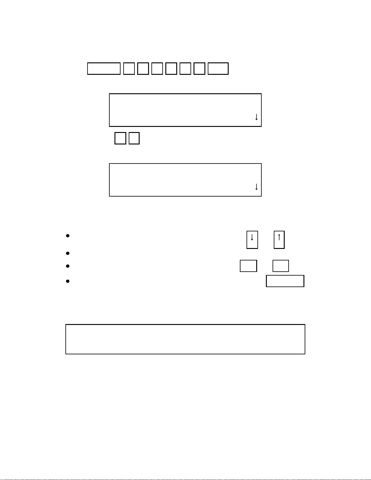
1.3 INSTALLATION PROCEDURE
This product is to be used with the Ricoh FAX5600L. Users of
this instruction document should be either service trained or
certified by successfully completing a Ricoh Technical Training
Program in English.
Tools Required
Metric Philips screw driver set PROM puller
Use the antistatic wrist strap as an antistatic safety measure during the
installation of this product.
NOTE: Before installing this option read the Operator Safety,
Laser Safety, and other notes, warnings and cautions at the
beginning of this machine's Service Manual.
Procedure
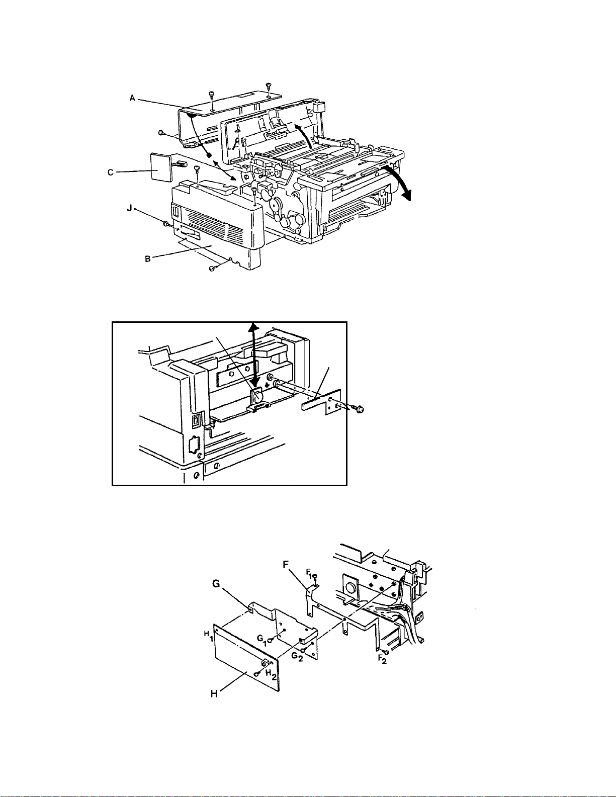
1. Turn off the fax machine power, and disconnect the machine.
2. Unfasten the rear cover, disconnect the speaker and remove the
back cover. Figure 1 [A].
3. Raise the front cover and scanner cover [release buttons front and
side].
4. Remove the left cover. Figure 1 [B].
5. Remove the MBU holder. Figure 2 [D]. The MBU holder will not be
reused.
MBU System ROM Replacement
6. Move the MBU battery jumper, TB1, to OFF.
7. Remove MBU System ROMs from their sockets:
FAX5600L IC 3 and IC 4
8. Replace with the G4 Digital Option ROMs:
FAX5600L IC 3 and IC 4
9. Move the battery jumper back to ON.
G4 "D" KIT Type 90 SM3
Page 5
[E]
Figure 1
Figure 2
44
Figure 3
[D]
G4 "D" KIT Type 90 SM4
Page 6
Grounding Plate and Bracket
10. Remove the NCU to attach the grounding plate. Figure 1 [C].
11. Attach the grounding plate using one tapping screw, and one
threaded screw. Figure 3 [F, F , F ].
1 2
NOTE: The threaded screw connects to ground.
12. Attach the mounting bracket using two tapping screws. Figure 3
[G, G , G ].
1 2
CVG4
13. Plug the CVG4 PWA connector, CN 1, into the FCU, and secure it
to the mounting bracket using two threaded screws. Figure 3
[H H ].
1, 2
14. Replace the NCU and the left cover. Figure 1 [B, C].
Modified Rear Cover
15. From the original rear cover, remove the speaker and, if installed,
the hard disk option cover and the memory card. Using the same
fasteners attach them to the new G4 cover.
16. Attach the new G4 cover to the machine.
Communication Cables
17. Orient the wire routing guide so that the cables will feed down
through the routing loop. Affix the guide above and to the right of
the rear screw on the left panel. Figure 1 [J].
18. Connect the V.35 data cable and the V.24-200 auto-dial cable to
the G4 networking equipment.
19. Feed the cables down through the routing loop. Twist the loop
ends together to secure the cables.
NOTE: The test switches located beneath the auto-dial
connector on the rear panel should all be OFF. These switches
are used in back-to-back testing only.
G4 "D" KIT Type 90 SM5
Page 7

Final Steps
20. Affix the new model label over the old model name on the operator
panel.
21. Connect the G4 cables to the G4 networking equipment.
22. Use the FAX5600L Installation Checklist, section 1.2 above, to
complete the initialization procedure on page 3-13 in the Service
Manual.
NOTE: Do not attempt to restore power until all connections
have been made.
Additional Equipment
Back-to-Back Cable Part Number 28433-001
A back-to-back cable capable of testing V.35 and V.24 signals is used for
the following V.35/V.24 tests.
1. The input port data. See Internal Switch 0F (ISW0F).
2. Back-to-back CSDN layer 1 and PSDN layer 2 network
simulations. See section 4 below.
X.21 is not supported in this product at this time, and the back-to-back
cable is not available.
G4 "D" KIT Type 90 SM6
Page 8
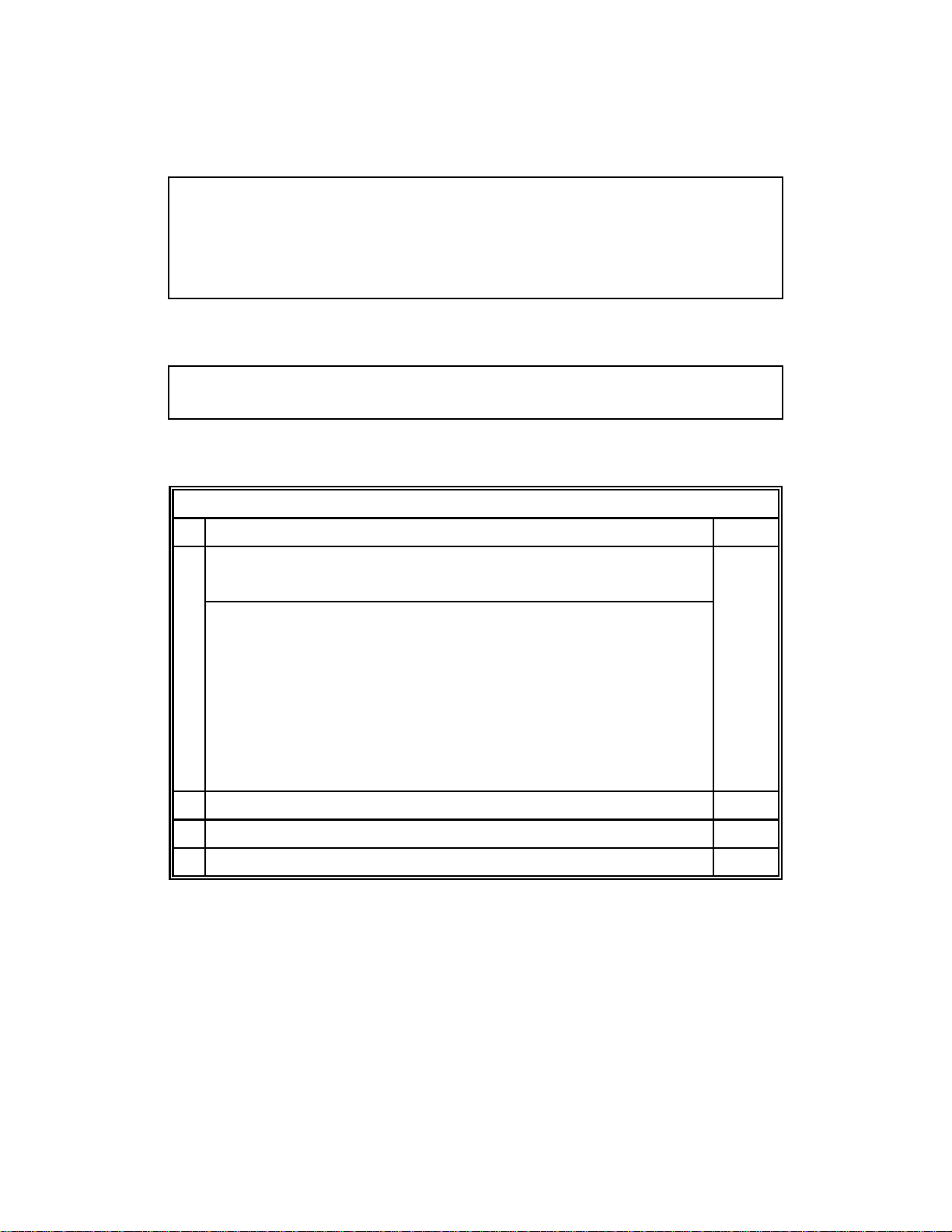
2 SERVICE TABLES AND PROCEDURES
2.1 SERVICE LEVEL FUNCTIONS
FUNCTION DESCRIPTION
01 G4_ISW : G4 Internal Switches, one of two sets of G4 software switches.
02
03 DN_IP : Not used in the United States. Do not modify.
04
05 G4_SN1 : G4 Subscriber Number 1, one of two G4 subscriber numbers.
06 G4_SN2 : Not used in the United States. Do not modify.
07 ~ 11 Not used.
12
13
14 Not used.
15 Prints the commands sent between the FCU and the CVG4 as the
G4_PSW : G4 Parameter Switches, the second of two sets of G4
software switches.
ISDN_IP : Integrated Services Data Network International Prefix.
A network access code, similar to the international dial access code, and
used to receive transfer result reports when communicating through a
terminal adapter to an ISDN network machine.
DNIC : Data Network Identification Code.
A four-digit code which identifies the network the terminal is on, and used
when communicating with a machine on another CSDN or PSDN
network.
G4_TID : G4 Terminal Identification Code.
A three-part code consisting of the network's country code, the terminal's
network number, and the terminal name, and used when communicating
through a terminal adapter to ISDN networks. It is similar to a TTI.
G4_DMP1 : G4 Memory Dump List.
contents of a specified range of memory locations
G4_DMP2 : G4 Protocol Dump.
16 Prints a list of protocol signals exchanged during the last communication.
See also bit switches ISW12-0 and PSW0E-1.
G4_LIST : G4 System Parameter List.
17 Prints a list showing the current G4 ISW and PSW bitswitch settings, and
other parameters programmed with G4 functions
18 Not used.
G4 "D" KIT Type 90 SM7
Page 9
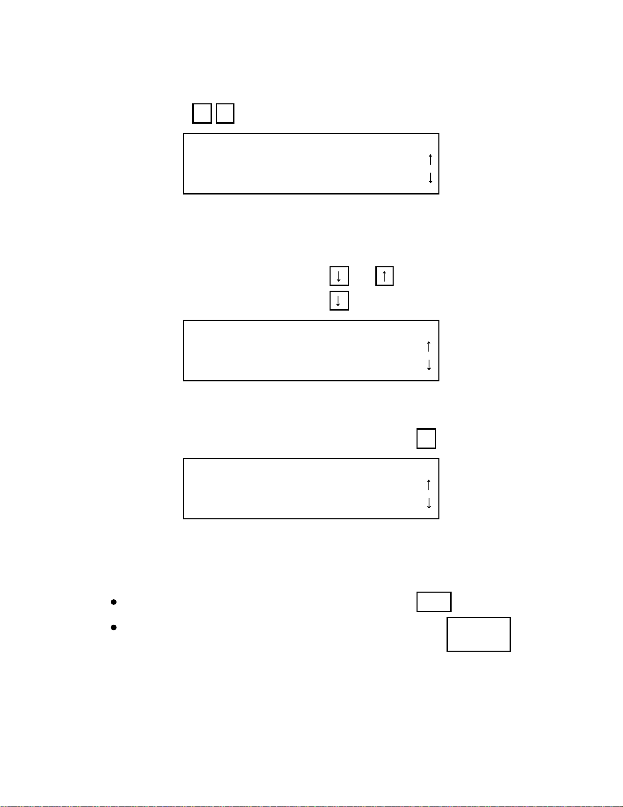
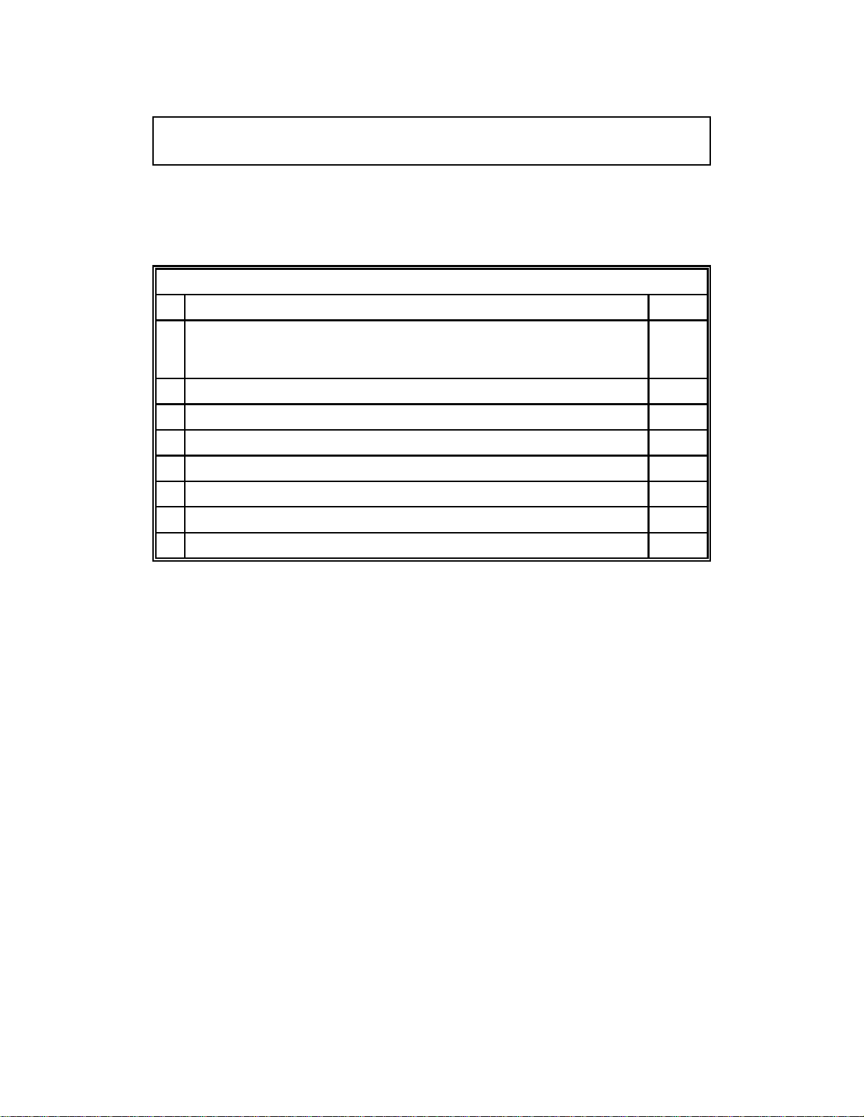
2.2 SERVICE LEVEL PROGRAMMING
1. To enter the G4 service mode, press
Function 6 0 1 9 9 1 Yes
The Service Function menu appears:
SERVICE FUNCTION NO.$$
01BIT SW. 02PARA LIST
03ERROR CODE 04SVC MONITOR
2. Press 1 8
The G4 service function menu appears:
G4 NO.$$
01.G4_ISW 02.G4_PSW
03.DN_IP 04.ISDN_IP
To review the menu pages, press the scroll and
keys
Use the ten key pad to enter numbers.
To return to the Service Function menu, press Yes or No
To exit the service modes and return to standby, press Function
SYSTEM RESET NOTE: The machine must be reset after
completing G4 service mode operations: Turn off the main
power to the machine; wait a few seconds; then turn it back on.
G4 "D" KIT Type 90 SM8
Page 10
2.2.1 ISW Internal Switch (Function 01)
1. Enter the G4 service mode.
Press 0 1
G4_ISW
DF: 00010001
SW:00 00010001
Bits are numbered from 0 to 7. Bit 7 is displayed at the left, and bit
0 at the right. The default settings (DF) are shown above the
current settings (SW).
2. To display another switch, press or
Example: To display bit switch 3, press 3 times
G4_ISW
DF: 00000000
SW:03 00000000
3. Press a bit 's number on the ten-key pad to toggle its setting
between 0 and 1.
Example: To change bit 3 from its current setting, press 3 once.
G4_ISW
DF: 00000000
SW:03 00001000
4. To continue adjusting bit switches, go to steps 2 and 3.
To return to the G4 service function menu, press Yes
To exit the service modes and return to standby, Function
press
and perform system reset.
G4 "D" KIT Type 90 SM9
Page 11
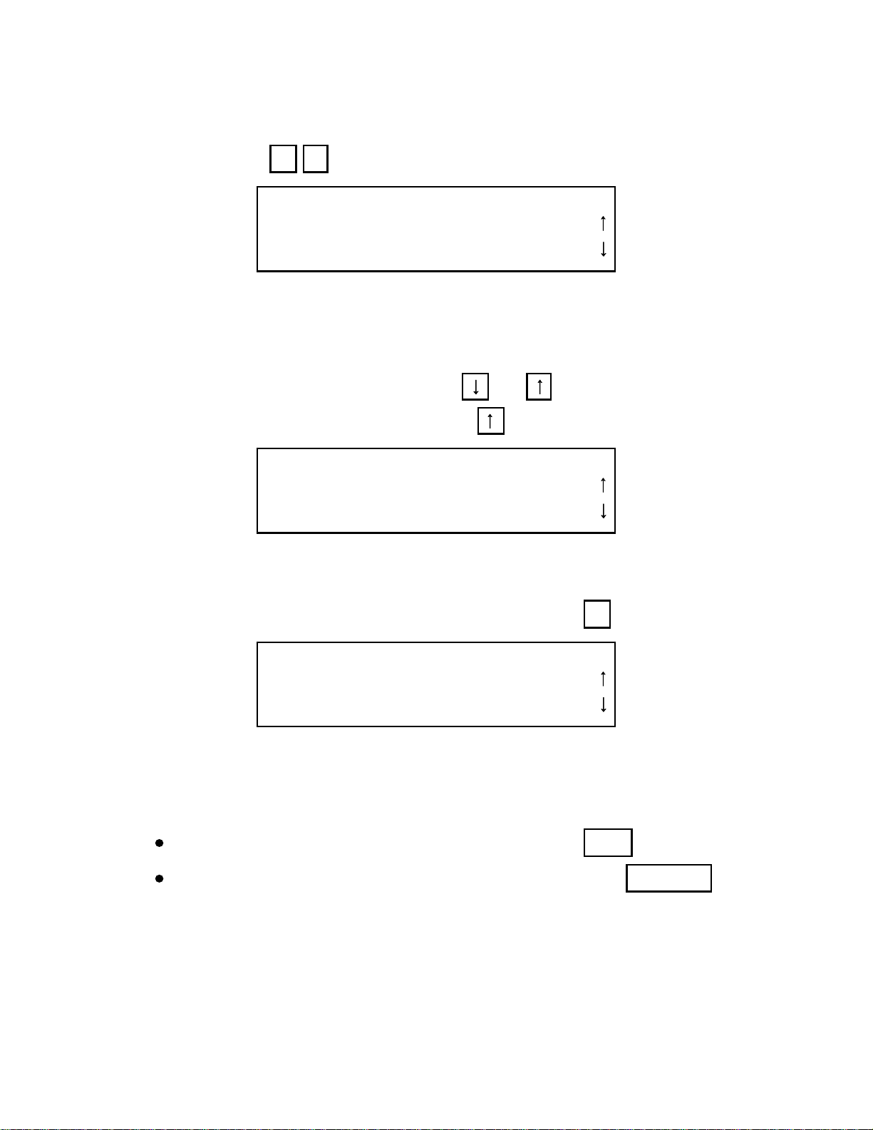
2.2.2 PSW Parameter Switch (Function 02)
1. Enter the G4 service mode.
Press 0 2
G4_PSW
DF: 01000000
SW:00 01000000
Bits are numbered from 0 to 7. Bit 7 is displayed at the left, and bit
0 at the right. The default settings (DF) are shown above the
current settings (SW).
2. To display another switch, press or
Example: To display bit switch 0E, press 2 times
G4_PSW
DF: 10110010
SW:0E 10110010
3. Press a bit 's number on the ten-key pad to toggle its setting
between 0 and 1.
Example: To change bit 0 from its current setting, press 0 once.
G4_PSW
DF: 10110010
SW:0E 10110011
4. To continue adjusting bit switches, go to steps 2 and 3.
To return to the G4 service function menu, press Yes
To exit the service modes and return to standby, press Function
and perform system reset.
G4 "D" KIT Type 90 SM10
Page 12
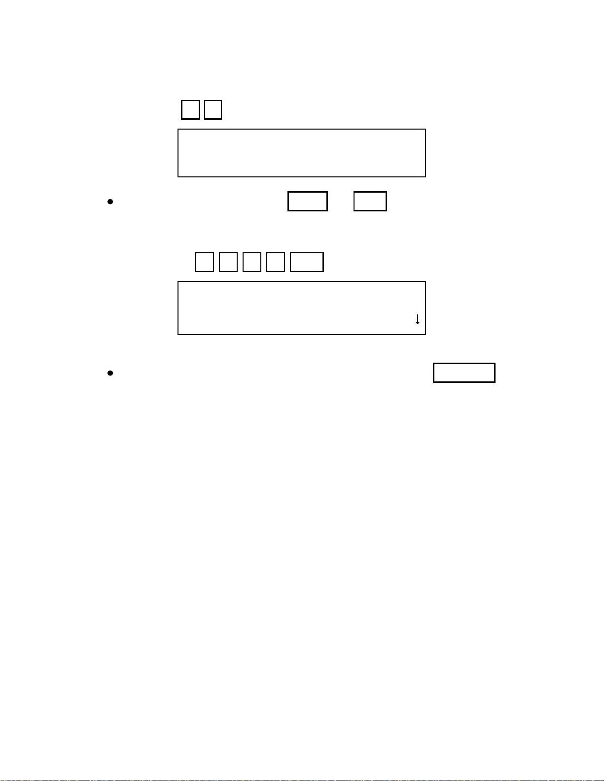
2.2.3 ISDN International Prefix (Function 04)
1. Enter the G4 service mode.
Press 0 4
ISDN_IP
$$$$
To change an entry, press Clear or No
2. Enter the code provided by the network.
Example: Press 1 2 3 4 Yes
G4 NO.$$
01.G4_ISW 02.G4_PSW
03.DN_IP 04.ISDN_IP
To exit the service modes and return to standby, press Function
and perform system reset.
G4 "D" KIT Type 90 SM11
Page 13
2.2.4 Subscriber Number 1 (Function 05)
1. Enter the G4 service mode.
Press 0 5
G4_SN1
$$$$$$$$$$$$$$$$$$$$
To change an entry, press Clear or No
2. Enter the the subscriber number (up to 20 digits), including a
pause (–).
Example: Press Pause 1 2 3 4 5 6 7 Yes
G4 NO.$$
01.G4_ISW 02.G4_PSW
03.DN_IP 04.ISDN_IP
To exit the service modes and return to standby, press Function
and perform system reset.
G4 "D" KIT Type 90 SM12
Page 14
2.2.5 DNIC Network Identification (Function 12)
1. Enter the G4 service mode.
Press 1 2
DNIC
$$$$
To change an entry, press Clear or No
2. Enter the code provided by the network.
Example: Press 1 2 3 4 Yes
G4 NO.$$
01.G4_ISW 02.G4_PSW
03.DN_IP 04.ISDN_IP
To exit the service modes and return to standby, press Function
and perform system reset.
G4 "D" KIT Type 90 SM13
Page 15
2.2.6 TID Terminal Identification (Function 13)
1. Enter the G4 service mode.
Press 1 3
G4_TID
-=
$$$$
To change an entry, press Clear or No
2. Enter the country code of the terminal. The US county code is 011.
Example: Press 0 1 1 Yes
G4_TID
011-=
–$$$$$$$$$$$$
3. Enter the terminal's fax number.
Example: Press 4 0 8 4 7 1 9 8 1 1 Yes
G4_TID
011-4084719811=
=$$$$$$$$$$$ ABC
4. Enter the terminal's identifcation provided by the customer.
Use the Quick Dial (QD) keys to enter letters, spaces (QD key 30)
and symbols (QD key 31).
Example: Press L 8 0 + D G 4 C C U
G4_TID YES OR CLR NO
011-4084719811=L80+DG4CCU
–L80+DG4CCU $$
5. Press Yes to program the entry and return to G4 service mode.
G4 "D" KIT Type 90 SM14
Page 16
2.2.7 Memory List Printing (Function 15)
This function disgorges the machine memory for engineering
development purposes; it is impractical to use in the technical service
environment. See Function 16 which prints a hex code listing of the
protocol exchange for a more useful tool.
1. Enter the G4 service mode.
Press 1 5
G4 MEMORY DUMP
ADD. $$$$ 00H — ADD. FFH
Use the Quick Dial keys to enter letters.
To erase an entry, press No
2. Enter the starting address of the range to be printed.
Example: Press 2 2 A A
G4 MEMORY DUMP
ADD.22AA00H — ADD. $$$$ FFH
3 Enter the final address of the range to be printed.
Example: Press 2 2 B B
G4 MEMORY DUMP
ADD.22AA00H — ADD.22BBFFH
PRESS "START"
4. Press Start to print the contents of the range.
G4 MEMORY DUMP
PRINTING
G4 "D" KIT Type 90 SM15
Page 17
5. When the list is printed, the display of step 1 reappears.
G4 MEMORY DUMP
ADD. $$$$ 00H — ADD. FFH
To return to the Service Function menu, press Yes or No
To exit the service modes and return to standby, press Function
2.2.8 Protocol List Printing (Function 16)
1. Enter the G4 service mode.
Press 1 6
G4_DMP2
0 PROTOCOL
PRESS "START"
2. Press Start to print.
G4 PROTOCOL DUMP LIST
PRINTING
3. When the list is printed, the display of step 1 reappears.
G4_DMP2
0 PROTOCOL
PRESS "START"
To return to the Service Function menu, press Yes or No
To exit the service modes and return to standby, press Function
G4 "D" KIT Type 90 SM16
Page 18
2.2.9 System Parameter List Printing (Function 17)
1. Enter the G4 service mode.
Press 1 7
G4 SYSTEM PARAMETER LIST
PRESS "START"
2. Press Start to print.
G4 SYSTEM PARAMETER LIST
PRINTING
3. When the list is printed, the G4 service function menu reappears.
G4 NO.$$
01.G4_ISW 02.G4_PSW
03.DN_IP 04.ISDN_IP
To return to the Service Function menu, press Yes or No
To exit the service modes and return to standby, press Function
G4 "D" KIT Type 90 SM17
Page 19
2.3 BIT SWITCHES
2.3.1 Internal Switches (ISW)
CAUTION
Do not adjust a bit switch that is described as "not used", as
this may cause the machine to malfunction, or to operate in a
manner that is not accepted by local regulations. Such bits are
for use only in other areas, such as Japan.
NOTE: Internal bit switches are changed using procedures
described in section 2.2.1.
Bit Switch ISW00
Bit Function Default
Country Code. Set 5 bit switches:
Bit 4 3 2 1 0 Country Bit 4 3 2 1 0 Country
0 0 0 0 0 France 0 1 0 1 0 Sweden
0 0 0 0 1 Germany 0 1 0 1 1 Switzerland
0 1
1 0
2 0
3 0
4 1
5 Not used. Do not change factory setting. 0
6 Not used. Do not change factory setting. 0
7 Not used. Do not change factory setting. 0
0 0 0 1 0 UK 0 1 1 0 0 Portugal
0 0 0 1 1 Italy 0 1 1 0 1 Holland
0 0 1 0 0 Austria 0 1 1 1 0 Spain
0 0 1 0 1 Belgium 0 1 1 1 1 Israel
0 0 1 1 0 Denmark 1 0 0 0 1 USA
0 0 1 1 1 Finland 1 0 0 1 0 Asia
0 1 0 0 0 Ireland 1 0 0 1 1 Japan
0 1 0 0 1 Norway
G4 "D" KIT Type 90 SM18
Page 20
NOTE: Bit switches ISW01 and ISW02 are not used in the United
States. Do not change the factory settings.
Bit Switch ISW03 (Application Task)
Bit Function Default
Frame Save Area Clear Mode (troubleshooting tool)
0 0: Clear with each communication 0
1: Not cleared
1 Debugging tool. Do not change factory setting. 0
2 Debugging tool. Do not change factory setting. 0
3 Debugging tool. Do not change factory setting. 0
4 Not used. Do not change factory setting. 0
5 Not used. Do not change factory setting. 0
6 Not used. Do not change factory setting. 0
7 Not used. Do not change factory setting. 0
Bit Switch ISW03 Comments:
Bit 0: Provides a save area of 2K bytes for communication protocols.
0: The area is cleared after each communication.
1: Saves communication exchanges until memory is used up. Exchanges are
printed with Function 16, G4 Protocol Dump.
G4 "D" KIT Type 90 SM19
Page 21
Rev.6/95
Bit Switch ISW04 (Data Link Task – Layer 2)
Bit Function Default
T3 time.The time in seconds (s) available to receive an acknowledging
frame sent in response to a command frame. When this time is 0
exceeded, the link channel is considered to be non-operational and will
0
be reset to continue normal link operations.
0: Ricoh mode T = 10 s.
1: CCITT T.90 (X.75) mode T = 30 s.
Shift-up Mode. Modulo 8 to modulo 128
1 0: Immediate (negotiation available) 0
1: Indirect (call disconnect/reconnect)
Fallback Mode. Modulo 128 to modulo 8
2 0: Immediate (negotiation available) 0
1: Indirect (call disconnect/reconnect)
3 Not used. Do not change factory setting. 0
4 Not used. Do not change factory setting. 0
5 Not used. Do not change factory setting. 0
6 Not used. Do not change factory setting 0
PSDN Back-To-Back Testing (Set one machine to 1) Reset after testing.
7 0: DTE 0
1: DCE
Bit Switch ISW04 Comments:
Bit 0: 0: T = 10 s. Sufficient time to ensure continuous link operations for most
circumstances.
1: T = 30 s. This setting is used for satellite communication paths, high traffic
congested networks, and when CCITT compliance is required for overseas
acceptance tests.
Bit 1: 0: Immediate. The DCE can respond to the modulo 8 SABM command frame
with DM, and will not disconnect the call. In turn, the modulo 8 machine shifts up
and sends the modulo 128 SABME link set up command frame.
1: Indirect. When SABM is received from the modulo 8 machine, the DCE
disconnects and does not send the DM frame. When the call is reconnected, the
modulo 8 machine shifts up and sends SABME to establish the data link.
Bit 2: 0: Immediate. The DCE can respond to the modulo 128 SABME command
frame with DM; the call is not disconnected. The modulo 128 machine will
fallback by sending SABM, the link setup command for modulo 8 machines.
1: Indirect. When SABME is received from a modulo 128 machine, the DCE will
disconnect the call. SABM is sent when the call is reconnected.
Bit 7: When doing a PSDN back-to-back test, one of the fax machines must appear to
be a DCE. This is done by setting this bit to 1 in one of the machines before
doing the test.
G4 "D" KIT Type 90 SM20
Page 22
Bit Switch ISW05 (Network Task – Layer 3)
Bit Function Default
Calling-up Packet
0 0: CR Packet (S:CR) Call Request 0
1: SQ Packet (S:SQ) Reset Request
1 Not used. Do not change factory setting. 0
Protocol ID Check
2 0: Yes (TYMNET) 0
1: No
3 Not used. Do not change factory setting 0
4 Not used. Do not change factory setting. 0
Received Charge (Collect Call)
5 0: Refuse 0
1: Accept
Ricoh Mode (57 second) Timer
6 0: Disabled 0
1: Enabled
Packet Size (P) and Window Size (W) T.90 CSDN (ISO8208)
7 0: Fixed 0
1: Variable
G4 "D" KIT Type 90 SM21
Page 23

Bit Switch ISW05 Comments:
Bit 0: This is used for packet networks and packet-type ISDNs. Between
communications, Call Request (CR) is used normally, but Reset Request (SQ)
can be used instead if this bit is at 1. If the network sends SQ, and if any packets
are stuck in the network (such as due to communication faults) between the two
terminals, they are cleared before communication. The setting of this bit depends
on the network; in general, if the network is not complete, set this bit to 1.
NOTE: Try setting this bit to 1 if layer 3 cannot be established.
Bit 2: The protocol ID is contained in the CR packet. This bit is set to 0 if the machine
is connected to TYMNET.
Bit 5: Collect calls known in the CCITT recommendations as "received charge". This is
only used for PSDNs and packet-type ISDNs. The CR packet informs whether or
not the call is a collect call.
0: Refuse collect call
1: Accept collect call
Bit 6: Ricoh 57-second timer. This is only for PSDN networks. Normally, if Call
Connected (CC) is not received in reply to CR within 180 seconds, the
communication is terminated. This time can be reduced to 57 seconds by setting
this bit to 1.
0: Disabled (normal time = 180 seconds)
1: Enabled
Bit 7: This bit can be set to 0 if the machine is connected to an ISDN through a
Terminal Adapter, or if it is connected to a CSDN that uses ISO8208 (T.90).
0: Fixed – Packet size (P) = 2048 Window size (W) = 7
1: Variable – As programmed in PSW07-0, 1, 2, 3, and PSW08-0,1,2,3 .
G4 "D" KIT Type 90 SM22
Page 24

Bit Switch ISW06 (Network Task – Layer 3)
Bit Function Default
S:CR Packet with Calling DTE Address
0 0: Disabled 0
1: Enabled
S:CR Packet with Calling and Receiving DTE Address
1 0: Disabled 0
1: Enabled
S:CR Packet with DNIC
2 0: Disabled 0
1: Enabled (FEDEX)
3 Not used. Do not change factory setting. 0
4 Not used. Do not change factory setting. 0
5 Not used. Do not change factory setting. 0
6 Not used. Do not change factory setting. 0
7 Not used. Do not change factory setting. 0
Bit Switch ISW06 Comments:
Bit 0: Inclusion of the sending DTE address in the Call Request packet (S:CR) – This
bit is only for packet networks. The CR packet should contain the receiving side's
DTE address; the transmitting side's may be included as an option.)
Bit 1: Inclusion of the transmitted/received DTE address in the S:CR packet – This bit
is only valid if the machine is connected to an ISDN through a Terminal Adapter,
or a T.90 CSDN; the CR packet is sent to match the IS8208 (T.90) layer 3
protocol. If the bit is 1, the other end's identifier can be seen in the display panel
a few seconds earlier than normal.
Bit 2: Inclusion of DNIC (DN)/CC (ISDN) in the S:CR packet – If the machine is
connected to the Federal Express network, this bit should be 1.
G4 "D" KIT Type 90 SM23
Page 25

Bit Switch ISW07 (Network Task)
Bit Function Default
Multi-channel (LCN Variability)
0 0: Contracted 0
1: Not contracted
International Prefix
1 0: Disabled 0
1: Enabled
Facility (Packet and Packet Window Size) Limitation
2 0: Disabled 0
1: Enabled
3 Not used. Do not change factory setting. 0
4 Not used. Do not change factory setting. 0
5 Not used. Do not change factory setting. 0
6 Not used. Do not change factory setting. 0
7 Not used. Do not change factory setting. 0
Bit Switch ISW07 Comments:
Bit 0: 0: Contracted – If the logical channel number (LCN) is set to a different number
(see PSW0A) from the actual value, communication is still possible.
1: Not contracted – Communication is not possible under the above conditions. It
may be necessary to set this bit to 1 to carry out certain PTT approval tests.
Bit 1: The setting of this bit depends on the network specifications.
Bit 2: 0: Packet and packet window sizes are as programmed:
(see packet, PSW07-0, 1, 2, 3 and packet window, PSW08-0, 1, 2, 3)
1: The packet window size (W) is fixed according to the packet size (P) as
follows: if P = 128, W = 5; if P = 256, W = 4; if P = 512, W = 2;
if P = 1024, W = 2. These match the Japanese DDX-P network specifications.
G4 "D" KIT Type 90 SM24
Page 26

NOTE: Bit Switches ISW08, ISW09, and ISW0A through D are
not used in the United States. Do not change the factory
settings.
Bit Switch ISW0E
Bit Function Default
Physical Mode
0 0: CCITT (V.24-200, X.21 dialing) 0
1: NTT DDX (Japan)
X.21 Dialing Mode*
1
0: Normal X.21 dialing mode
1: Enabled
V.25 (V.24-200) Auto Dial
2 0: Disabled 0
1: Enabled (SEP code)
Rough Timer Mode
3 0: Off 0
1: On
4 Not used. Do not change factory setting. 0
5 Not used. Do not change factory setting. 0
6 Not used. Do not change factory setting. 0
7 Not used. Do not change factory setting. 0
Bit Switch ISW0E Comments:
Bit 0: 0: CCITT:
a) At the end of dialing on the V.24-200 parallel autodial interface, EON is used.
b) For X.21, there is no CPS (Call Progress Signal) start code.
1: DDX:
a) At the end of dialing on the V.24-200 interface, + is used.
b) For X.21, CPS start code, SI, is checked.
0
Bit 1: 0: Normal X.21 dialing is used
1: A prefix of "5/16-" is added at the start of the number. This is used on the
DATEX-L network in Germany.
Bit 2: If the user wishes to connect the machine to the PSTN with a V.25 interface
(V.24-200 parallel autodial), setting this bit to 1 will cause the machine to
automatically insert the "SEP" code at the start of the telephone number.
Bit 3: For machines with a V.24-200 autodial, the rough timer provides a timing
adjustment to overcome problems that some DCEs exhibit when working through
this interface.
* Not applicable at this time
G4 "D" KIT Type 90 SM25
Page 27

Rev. 6/95
Bit Switch ISW0F
Bit Function Default
0 Not used. Do not change factory setting. 0
1 Not used. Do not change factory setting. 0
L1 Timing Signal Check in PSDN Back-to-Back Test
2 0: Disabled 0
1: Enabled
Call Detection Mode. Set 2 bits:
Bit: 4 3 Mode
3 0 0 CI: On only 0
4 1 0 CI or CD: On (DTR: On) 0
0 1 CI or CD: On (RTS: On)
1 1 Reserved
CVG4 I/O Port Check Mode. Set 2 bits:
Bit: 6 5 Mode
5 0 0 Normal operation 0
6 1 0 Output "H" data on IO ouput port 0
0 1 Output "L" data on IO output port
1 1 Indicate input port data on LCD
7 Not used. Do not change factory setting. 0
Bit Switch ISW0F Comments:
Bit 2: Enable this bit to check the Layer 1 timing signals (TX: ST2 and RX: RT) during
Layer 2 back-to-back testing in order to study compatibility with the network
DSU.
If the back-to-back test is successful when this bit is enabled, but the network
communication is not, the data transfer timing signals may not be compatible
with those of the DSU. (REF: PK Type 1 test, FAX7000D Service Manual, pages
3-6 and 6-22)
Reset this bit to 0 after testing. See section 4 and PSW0D, for test procedures.
Bits 3 and 4: Method of entering receive mode in V series communication. The setting
of these bits depends on the type of DSU or DCE.
Bits 5 and 6: Terminal board test – This can test the operation of each signal on the
V.24(V.28), V.35, or X.21* jack. The procedures follow.
* Not applicable at this time
G4 "D" KIT Type 90 SM26
Page 28

Test Procedure for bits 5 and 6
NOTE: When all testing is done, restore the dip switches to OFF,
the bit switches for normal operation, and reset the machines:
See System Reset Note, page 8.
Output "H" data on IO output port (all output pins high – ISW0F = 01000000):
Disconnect the machine from the DCE. Set the CVG4 dip switches below the dial
connector to on. Then, set bits 5 and 6 of switch ISW0F to 0 and 1 respectively. Reset
the machine: hold down the Stop key for about 12 seconds. The output pins of the
machine will all read high on a multimeter.
Output "L" data on IO output port (All output pins low – ISW0F = 00100000):
The test procedure for output low is the same as for output high. In this case, set ISW0F5 and 6 to 1 and 0 respectively.
Input Port Data on LCD (Machine Input Test Mode) – Test 1:
Connect two machines with the V.35/V.24(V.28) back-to-back cable. CVG4 dip switches
can be on or off.
On the machine to be tested, set ISW0F-5 and 6 to 1 (01100000). On the other machine,
set bits 5 and 6 for either "output high" (01000000) or "output low" (00100000). Then
reset both machines: hold down the Stop key for about 12 seconds.
The output pins on the other machine will go high if "ouput high" was selected (or low, if
"output low" was selected), causing the input pins on the tested machine to go high (or
low). On the tested machine, the following pins should go high (or low):
V.35: D(CS), E(DR), F(CD), J(CI), R(RDA), T(RDB)
V.24 (V.28): 3(RD), 5(CS), 6(DR), 8(CD), 22(CI)
V.24-200 (Auto Dial): 3(ACL), 5(PND), 13(DSC), 22(DLO)
X.21: 4(RA), 5 (IA), 11(RB), 12(IB) *
* Not applicable at this time
G4 "D" KIT Type 90 SM27
Page 29

LCD Display
The display in the bottom right of the LCD shows the status of the input pins as a
four-figure (two-byte) hexadecimal code. (This code is displayed one byte at a time; the
high byte is displayed for 2 seconds, and the low byte is displayed for 1 second, and this
is repeated indefinitely). the make-up of this code depends on the status of the input pins
as shown in the following table:
Bit Meaning Bit Meaning
1:V.24-200 PND Low 8
0
1 1:V.24-200 ACL Low 9 Not used
2 1:V.24-200 DSC Low 10 Not used
3 1:V.24-200 DLO Low 11 Not used
4 1:V.24, V.35 CD Low 12 Not used
5 1:V.24, V.35 CI Low 13 Not used
6 1:V.24, V.35 CS Low 14 Not used
7 1:V.24, V.35 DR Low 15 1: Rx data Low
Correct output codes are as follows:
1:X.21 IA and IB High*
V.35 V.24(V.28) V.24-200
HIGH 7F0F 7F0F 7F8F 7FFF
LOW FFFF FFFF FFFF FEFF
Input Port Data on LCD (Machine Input Test Mode) – Test 2:
Disconnect the machine from the DCE. Then set ISW0F-5 and 6 to 1 (01100000). Hold
down the Stop button for about 12 seconds. If the test is correct, the display in the
bottom right corner of the LCD should be as follows:
V.35 or X.21*: 7FFF V.24(V.28): FFFF
X.2I*
* Not applicable at this time
G4 "D" KIT Type 90 SM28
Page 30

NOTE: Internal switches ISW10 and ISW11 are not used in the
United States. Do not change the factory settings.
Bit Switch ISW12
Bit Function Default
Frame Save Conditions for G4 Protocol Dump List
0 0: Excludes layer 2 signals when C/R save mode (PSW0E) is on 0
1: Includes layer 2 signals when C/R save mode (PSW0E) is off
1 Not used. Do not change factory setting. 0
2 Not used. Do not change factory setting. 0
3 Not used. Do not change factory setting. 0
4 Not used. Do not change factory setting. 0
5 Not used. Do not change factory setting. 0
6 Not used. Do not change factory setting. 0
7 Not used. Do not change factory setting. 0
Bit Switch ISW12 Comments:
Bit 0: 0: When ISW12-0 is 0, and PSW0E-1 is 1, the G4 protocol dump list will not
include data link layer command/response (C/R) protocols.
1: When ISW12-0 is 1, and PSW0E-1 is 0, the G4 protocol dump list will include
data link layer command/response protocols, such as Receive Ready (RR) or
Set Asychronous Balanced Mode (SABM).
Use G4 function 16 to print a G4 protocol dump list, and see section 2.3.2 for
bitswitch PSW0E-1.
NOTE: Internal switches ISW13 through 19, and ISW1A through
1F are not used in the United States. Do not change the factory
settings.
G4 "D" KIT Type 90 SM29
Page 31

2.3.2 Parameter Switches (PSW)
CAUTION
Do not adjust a bit switch that is described as "not used", as
this may cause the machine to malfunction, or to operate in a
manner that is not accepted by local regulations. Such bits are
for use only in other areas, such as Japan.
NOTE: Parameter bit switches are changed using procedures
described in section 2.2.2.
Bit Switch PSW00
Bit Function Default
0 Not used. Do not change factory setting. 0
1 Not used. Do not change factory setting. 0
Network
2 0: CSDN (Circuit Switched)
1: PSDN (Packet Switched)
0
3 Not used. Do not change factory setting. 0
DCE I/F Dial
4 0: Auto Dial
1: Manual
DCE I/F Data. Set 2 bits.
Bit: 6 5 I/F
5 0 0
6 0 1
1 0
7 Not used. Do not change factory setting 0
Bit Switch PSW00 Comments:
Bit 2: Set this bit at installation to match the network connection.
Bit 4: Set this bit at installation to match the type of dialing connection between the
machine and the DCE.
Bits 5 and 6: Set these two bits at installation to match the type of data connection
X.21*
V.24 (V.28)
V.35 (V.10, V.11)
between the machine and the DCE.
* Not applicable at this time
0
0
1
G4 "D" KIT Type 90 SM30
Page 32

NOTE: Parameter switches PSW01 and PSW02 are not used in
the United States. Do not change the factory settings.
Bit Switch PSW03
Bit Function Default
Link Modulus
0 0: Modulo 8 0
1: Modulo 128
1 Not used. Do not change factory setting. 0
2 Not used. Do not change factory setting. 0
3 Not used. Do not change factory setting. 0
4 Not used. Do not change factory setting. 0
5 Not used. Do not change factory setting. 0
6 Not used. Do not change factory setting. 0
7 Not used. Do not change factory setting. 0
Bit Switch PSW03 Comments:
Bit 0: The link modulus determines the protocol frame numbering method.
Modulo 8 uses 3 bits, numbering from 0 to 7 and starting again at 0.
Modulo 128 uses 7 bits, numbering from 0 to 127 and starting again at 0.
0: Modulo 8 is the normal CSDN and PSDN setting.
1: Modulo 128 can be used when large amounts of data are to be transmitted
over error-free lines.
Check with the network company for the appropriate setting.
G4 "D" KIT Type 90 SM31
Page 33

Bit Switch PSW04
Bit Function Default
Link K Value. Set 4 bits.
Bit: 3 2 1 0 Value Bit: 3 2 1 0 Value
0 0 0 0 0 1 0 0 0 8
0 0 0 1 1 1 0 0 1 9
0 0 0 1 0 2 1 0 1 0 10 1
1 0 0 1 1 3 1 0 1 1 11 1
2 0 1 0 0 4 1 1 0 0 12 1
3 0 1 0 1 5 1 1 0 1 13 0
0 1 1 0 6 1 1 1 0 14
0 1 1 1 7 1 1 1 1 15
4 Not used. Do not change factory setting. 0
5 Not used. Do not change factory setting. 0
6 Not used. Do not change factory setting. 0
7 Not used. Do not change factory setting. 0
Bit Switch PSW04 Comments:
Bits: 0, 1, 2, and 3: These bits are set, along with the link modulus PSW03-0 bit
switch, according to network specifications. The link K value is
the maximum number of unacknowledged frames that the
machine can send out before having to pause and wait for an
acknowledgement from the other end.
If the link modulus (PSW03-0) is set to modulo 8, the K value
cannot be more than 7. If the link modulus is set to modulo 128,
the K value can be up to 15.
G4 "D" KIT Type 90 SM32
Page 34

Bit Switch PSW05
Bit Function Default
Link Timer Value. Set 4 bits.
Bit: 3 2 1 0 Value Bit: 3 2 1 0 Value
0 0 0 0 0
0 0 0 0 1 1 0
1 0 0 1 0 2 1
2 0 0 1 1 3 0
3 0 1 0 0 4 0
0 1 0 1 5
0 1 1 0 6
0 1 1 1 7
1 0 0 1 8
1 0 0 1 9
1 0 1 0 10
4 Not used. Do not change factory setting. 0
5 Not used. Do not change factory setting. 0
6 Not used. Do not change factory setting. 0
7 Not used. Do not change factory setting. 0
Bit Switch PSW05 Comments:
Bits: 0, 1, 2, and 3: The link timer value is the maximum allowable time between
sending a protocol frame and receiving a response frame from
the DSU. Normally, a setting of 2 is enough. A higher value may
be necessary for a network using satellites.
G4 "D" KIT Type 90 SM33
Page 35

Bit Switch PSW06
Bit Function Default
Layer 3 Protocol
0 0: IS8208 0
1: T.70 Null
1 Not used. Do not change factory setting. 0
2 Not used. Do not change factory setting. 0
3 Not used. Do not change factory setting. 0
Packet Modulus
4 0: Modulo 8 0
1: Modulo 128
5 Not used. Do not change factory setting. 0
6 Not used. Do not change factory setting. 0
7 Not used. Do not change factory setting. 0
Bit Switch PSW06 Comments:
Bit 0: 0: PSDN or CSDN T.90 connection
1: CSDN
Bit 4: This bit function is similar to the link modulus, PSW03-0; it determines the packet
numbering method for PSDN connections. Normally, modulo 8 is used. Modulo
128 is useful when large amounts of data are to be transmitted over error-free
lines. Check with the network company for the appropriate setting.
G4 "D" KIT Type 90 SM34
Page 36

Bit Switch PSW07
Bit Function Default
Packet Size. Set 4 bits.
Bit: 3 2 1 0 Value
0 1
1 1
2 0
3 1
0 1 1 1 128
1 0 0 0 256
1 0 0 1 512
1 0 1 0 1024
1 0 1 1 2048
4 Not used. Do not change factory setting. 0
5 Not used. Do not change factory setting. 0
6 Not used. Do not change factory setting. 0
7 Not used. Do not change factory setting. 0
Bit Switch PSW07 Comments:
Bits: 0, 1, 2, and 3: The packet size depends on the memory size of the packet
handling equipment in the network. Set these bits according to
the network specifications.
G4 "D" KIT Type 90 SM35
Page 37

Bit Switch PSW08
Bit Function Default
Packet Window Size. Set 4 bits.
Bit: 3 2 1 0 Value Bit: 3 2 1 0 Value
0 0 0 0 0 1 0 0 0 8
0 0 0 1 1 1 0 0 1 9
0 0 0 1 0 2 1 0 1 0 10 0
1 0 0 1 1 3 1 0 1 1 11 1
2 0 1 0 0 4 1 1 0 0 12 0
3 0 1 0 1 5 1 1 0 1 13 0
0 1 1 0 6 1 1 1 0 14
0 1 1 1 7 1 1 1 1 15
4 Not used. Do not change factory setting. 0
5 Not used. Do not change factory setting. 0
6 Not used. Do not change factory setting. 0
7 Not used. Do not change factory setting. 0
Bit Switch PSW08 Comments:
Bits: 0, 1, 2, and 3: A setting for PSDN, which is similar to the Link K parameter set
by PSW04-0, 1, 2, and 3. It is used for the maximum number of
packets the machine can send without receiving a response from
the other end. If IS8208 layer 3 protocol was selected by
PSW06-0, the maximum value is 7.
G4 "D" KIT Type 90 SM36
Page 38

Bit Switch PSW09
Bit Function Default
LCGN. Set 4 bits.
Bit: 3 2 1 0 Value Bit: 3 2 1 0 Value
0 0 0 0 0 1 0 0 0 8
0 0 0 1 1 1 0 0 1 9
0 0 0 1 0 2 1 0 1 0 10 0
1 0 0 1 1 3 1 0 1 1 11 0
2 0 1 0 0 4 1 1 0 0 12 0
3 0 1 0 1 5 1 1 0 1 13 0
0 1 1 0 6 1 1 1 0 14
0 1 1 1 7 1 1 1 1 15
4 Not used. Do not change factory setting. 0
5 Not used. Do not change factory setting. 0
6 Not used. Do not change factory setting. 0
7 Not used. Do not change factory setting. 0
Bit Switch PSW09 Comments:
Bits: 0, 1, 2, and 3: The Logical Channel Group Number (LCGN) provides packet
routing information over a switched data path within the packet
network. It indicates the Packet Assembler/Disassembler (PAD)
connection. It is used for PSDNs and ISDNs when there is more
than one channel to the network. The value is determined by
contract between user and network. If there is no contract, the
factory setting can be used.
G4 "D" KIT Type 90 SM37
Page 39

Bit Switch PSW0A
Bit Function Default
LCN. Set 8 bits.
Bit: 7 6 5 4 3 2 1 0 Value
0 0 0 0 0 0 0 0 0
0 0 0 0 0 0 0 1 1
0 0 0 0 0 0 1 0 2
0 0 0 0 0 0 1 1 3
0 0 0 0 0 1 0 0 4
0 0 0 0 0 1 0 1 5
0
1
2
3
4
5
6
7
0 0 0 0 0 1 1 0 6
0 0 0 0 0 1 1 1 7 1
0 0 0 0 1 0 0 0 8 0
0 0 0 0 1 0 0 1 9 0
0 0 0 0 1 0 1 0 10 0
0 0 0 0 1 0 1 1 11
0 0 0 0 1 1 0 0 12 0
0 0 0 0 1 1 0 1 13 0
0 0 0 0 1 1 1 0 14 0
0 0 0 0 1 1 1 1 15 0
0 0 0 1 0 0 0 0 16
1 1 1 1 1 1 0 1 253
1 1 1 1 1 1 1 0 254
1 1 1 1 1 1 1 1 255
Bit Switch PSW0A Comments:
The Logical Channel Number (LCN) is part of the packet routing information similar to the
LCGN (PSW09).
G4 "D" KIT Type 90 SM38
Page 40

Bit Switch PSW0B
Bit Function Default
Transport Block Size. Set 4 bits.
Bit: 3 2 1 0 Value
0 1
1 1
2 0
3 1
0 1 1 1 128
1 0 0 0 256
1 0 0 1 512
1 0 1 0 1024
1 0 1 1 2048
4 Not used. Do not change factory setting. 0
5 Not used. Do not change factory setting. 0
6 Not used. Do not change factory setting. 0
7 Not used. Do not change factory setting. 0
Bit Switch PSW0B Comments:
Bits: 0, 1, 2, and 3: The transport block size depends on the memory size of the
packet handling equipment in the network. It must not be greater
than the packet size value set by PSW07-0, 1, 2, and 3. Set
these bits according to the network specifications.
G4 "D" KIT Type 90 SM39
Page 41

Bit Switch PSW0C
Bit Function Default
Session Window Size. Set 2 bits:
Bit: 1 0 Value
0 0 1 1 1
1 1 0 2 0
1 1 3
2 Not used. Do not change factory setting. 0
3 Not used. Do not change factory setting. 0
4 Not used. Do not change factory setting. 0
5 Not used. Do not change factory setting. 0
6 Not used. Do not change factory setting. 0
7 Not used. Do not change factory setting. 0
Bit Switch PSW0C Comments:
Bits 0 and 1: This is the number of session layer commands that the machine can
send without receiving acknowledgment from the other end. CCITT
recommendations allow for a value up to 3, but keep the setting at 1 in
this machine.
G4 "D" KIT Type 90 SM40
Page 42

Rev. 6/95
Bit Switch PSW0D
Bit Function Default
Back-to-Back Test Mode. Set 4 bits.
Bit: 2 1 0 Test
0 0
1 0
2 0
0 0 0 Off for normal operation
1 0 0 Packet Back-to-Back (PSDN)
1 0 1 Layer 1 Test (CSDN)
0 1 0 Layer 2 test (CSDN)
3 Not used. Do not change factory setting. 0
4 Not used. Do not change factory setting. 0
5 Not used. Do not change factory setting. 0
6 Not used. Do not change factory setting. 0
7 Not used. Do not change factory setting. 0
Bit Switch PSW0D Comments:
See section 4 for back-to-back test procedures.
Bits 0, 1, and 2: 000: Normal Operation. Always reset the bits to 0000 after testing.
001: CSDN Layer 1 (Physical Link). This test checks data
transmission (ST2) and reception (RT) signal element timing for
the V.24 and V.35 physical connections. Signalling proceeds from
layer 1 when Start is pressed. The clock must be enabled in one
of the machines by setting dip switches as indicated in the section 4.
010: CSDN Layer 2 Back-to-Back Test (Data Link). This test doesn't
check layer 1 signal element timing. The clock must be enabled in one of
the machines by setting its dip switches. See section 4. Layer 1 is
established, and signalling begins from layer 2 when Start is pressed. This
setup is also used for high speed operation without a network, using DSUs
on a leased or dedicated line (no manual dialing).
010: CSDN Layer 2 Network Test (Data Link). Each machine is
connected to a network through a DSU. Connection between the DSUs
must be established before beginning the test-dialing is manual only.
Layer 1 is not checked. Clock signal is provided by the network: all the dip
switches are set to OFF.
100: PSDN Packet Back-to-Back Test. One machine must be set as DCE
(ISW04-7). Signal element timing (layer 1) is not checked. Clock is
enabled by setting the dip switches in one of the machines. See section 4.
Layer 2 is established when the machine is turned on, and SQ/SF (Reset
Request/Reset Confirm) packets are exchanged. Communication begins
from the CR (Call Request) packet, when Start is pressed.
100: PSDN Packet Network Test. Each machine is connected to a
network through a DSU. Connection between the DSUs must be
established before beginning the test. DCE does not need to be set, and
clock is provided by the network. SQ/SF packets are exchanged and
communication begins with the CR packet when Start is pressed.
G4 "D" KIT Type 90 SM41
Page 43

Rev. 6/95
Bit Switch PSW0E
Bit Function Default
Real Time Display (troubleshooting tool)
0 0: Off
1: On
Command/Response Frame Save (troubleshooting tool)
1 0: Off
1: On
2 Not used. Do not change factory setting. 0
3 Not used. Do not change factory setting. 0
Test Clock Rate. Set 4 bits.
Bit: 7 6 5 4 Rate (kbps) Bit: 7 6 5 4 Rate (kbps)
0
1
4 0 0 1 0 4.8 1
0 0 0 1 2.4
5 0 0 1 1 7.2 1
6 0 1 0 0 9.6 0
7 0 1 0 1 12.0 1
0 1 1 0 14.4
Bit Switch PSW0E Comments:
Bit 0: Set to 1 to display a status code in the bottom right of the character display. See section
6.1. for status codes.
Bit 1: Command/Response frames are saved when set to 1. When bit switch ISW12-0
is also set to1, Layer 2 command/response protocols will be included when the G4
protocol dump list is printed.
0: Off. When ISW12-0 is also set to 0 (off), the layer 2 protocols will not be printed.
1: On When ISW12-0 is also set to 1 (on), the layer 2 protocols will be printed.
Bits 4, 5, 6, and 7: This is used in back-to-back tests. (The default is 64.0 kbps.)
0 1 1 1 16.0
1 0 0 0 19.2
1 0 0 1 48.0
1 0 1 0 56.0
1 0 1 1 64.0
NOTE: Parameter switch PSW0F is not used. Do not change
the factory settings.
G4 "D" KIT Type 90 SM42
Page 44

3 G4 SERVICE RAM ADDRESSES
Additional service switch bits have been assigned for G4 network selection and
G4 transfer result report DNIC number.
Access the RAM addresses with G3 Service Level Function 06
(Service Manual, sections 4.1 and 4.1.6.)
FAX5600L
08005A (Service Switch 1A):
Bit 7: DNIC number for transfer result report 0: Enabled, 1: Disabled
08005B (Service Switch 1B):
Bit 5: Network selection for broadcasting numbering feature
0: DDX, 1: ISDN
Default Settings
FAX5600L
SW1A 0 0 0 0 0 0 0 0 Hex: 00
SW1B 0 0 0 0 0 0 1 0 Hex: 02
G4 "D" KIT Type 90 SM43
Page 45

4 BACK-TO-BACK TEST
NOTE: When testing is done, turn the dip switches to OFF, restore bit
switches to normal operation, and reset the machines: hold down
the STOP button for about 12 seconds. See System Reset Notes, page
8.
These tests are useful for demonstrations, training coursed, and machine testing
and troubleshooting. A cable rated for both V.35 and V .24 is used to connect
the machines directly to each other, back-to-back. The layer 2 test can be used
for compatibility problems: If the layer 2 test was successful but communication
was not, the machine's data transfer timing signals may be incompatible with
those of the DSU.
CSDN Layer 1 (Physical Link) Test - Direct
Two machines using CSDN protocol are directly connected to each other with
the V.35/V.24 back-to-back cable. The bit switches for the CSDN layer 1 test
mode and the cable rate are selected. The dip switches of ONE of the machines
are set to enable the clock. After the document has been placed in the ADF, the
call is initiated at the machine. Signalling begins when Start is pressed. The
layer 1 data transfer signal element timing pins, ST and RT, for V.24 and V.35
connections are tested.
CSDN Layer 2 (Data Link) Test - Direct
Two machines using CSDN protocol are directly connected to each other with
the V.56/V.24 back-to-back cable. The bit switches for the CSDN layer 2 test
mode and the cable rate are selected. The dip switches of ONE of the machines
are set to enable the clock. With the document in position in the ADF, the call is
initiated at the machine. Signalling stars from layer 2 when the Star button is
pressed. incompatibilllty is ignored, and layer 1 is established. Data transfer
signal element timing is NOT tested.
PSDN Packet test Direct
This test is a version the CSDN direct test above. Two machines using PSDN
protocol are directly connected to each other with the V.35/V.24 back-to-back
cable. The PSDN test mode and the cable rate are selected by bit switch. The
dip switches are set to enable the clock. In addition, for the back-to-back PSDN
test only, one of the machines is set as DCE. the physical link and the data link
are established at power up. Network layer Reset Request (SQ) and Reset
Confirmation (SF) packets are exchanged, and communicating begins with the
Call Request (CR) packet when the Start button is pressed.
G4 "D" KIT Type 90 SM44
Page 46

Back-to-back: CSDN Layer 1 &2/PSDN Packet Test-Direct
1. Turn off the AC power to both machines
2. Connect two fax machines through the data connectors with the
V.35/V.24 back-to-back cable.
3. Locate dip switches 1 through 8 above the dial connector on the CVG4.
On one of the machines, set the dip switches to enable the clock for V.35
or V.24 test mode:
-V.35 set 5,6,7,8, on.
-V.24 set 3,4, on.
All other switches should be off.
4. Turn the power on. Set the test mode (PSW0D), the cable data rate
(PSW00), and the PSDN DCE (ISW04) bit switches as required for the
test. The layer 1 signal element timing check can be enabled for layer 2
tests by setting bit switch ISW0F-2 to 1.
Enter the G4 service mode (section 2.2) and use G4 service mode
functions 01 and) 02 to set the switches as follows:
SWITCH MACHINE 1 MACHINE 2
ISW04 (DCE) 10000000 00000000
PSW0D (Test Mode)
CSDN Layer 1 00000001 00000001
CSDN Layer 2 00000010 00000010
PSDN Packet 00000100 00000100
PSW00 (Cable I/F)
V.35 01000000 01000000
V.24 00100000 00100000
ISW04 (DCE PSDN 10000000 00000000
only)
ISW04 (L1 Check in L2)* 00000100 00000100
*Optional
NOTE: Test clock rates can be set from 2.4 kbps to 64 kbps by bit
switch PSW0E. The default value is 64 kbps.
5. Enter G4 Service Mode.
6. Reset both machines by pressing the Stop button for 12 seconds.
7. Place a document in the ADF. Select G4 and dial by pressing any number
on the keypad. Press the Start button.
8. After completing the tests, restore the bit switches to their original
settings. Set the dip switches back to OFF.
9. Reset both machines by pressing the Stop button for 12 seconds.
G4 "D" KIT Type 90 SM45
Page 47

10. Exit the service mode. (See section 2.2)
5 SESSION LAYER SIGNAL IDENTIFIERS
5.1 LAYER 1 — PHYSICAL LAYER
5.1.1 V.35 Cable (X.21bis)
DB36 Signal V.35 DCE
1 RTA V From Rx Signal Element Timing
2 RTB X From Rx Signal Element Timing
3 ST2A Y From Tx Signal Element Timing
4 ST2B AA From Tx Signal Element Timing
5 ~ 18 Not Connected
19 FG A Frame Ground
20 SG B Signal Ground
21 RS C To Request to Send (RTS)
22 CS D From Clear to Send (CTS)
23 DR E From Data Set Ready (DSR)
24 CD F From Data Carrier Detect
25 ER H To Data Terminal Ready (DTR)
26 CI J From Call (Ring) Indication (RI)
27 TI NN From DCE Self Test Indicator
28 SDA P To Send Data
29 SDB S To Send Data
30 RDA R From Receive Data
31 RDB T From Receive Data
32 ~ 36 Not Connected
G4 "D" KIT Type 90 SM46
Page 48

5.1.2 V.24 Cable (X.21bis)
DB36 Signal V.24 DCE
1 ~ 6 Not Connected
7 SD 2 To Send Data
8 RD 3 From Receive Data
9 RT 17 From Rx Signal Element Timing
10 ST2 15 From Tx Signal Element Timing
11 ~ 18 Not Connected
19 FG 1 Frame Ground
20 SG 7 Signal Ground
21 RS 4 To Request to Send (RTS)
22 CS 5 From Clear to Send (CTS)
23 DR 6 From Data Set Ready (DSR)
24 CD 8 From Data Carrier Detect
25 ER 20 To Data Terminal Ready (DTR)
25 CI 22 From Call (Ring) Indication (RI)
27 TI 25 From DCE Self Test Indicator
28 ~ 36 Not Connected
G4 "D" KIT Type 90 SM47
Page 49

5.1.3 V.24-200 Cable (CSDN, CSDN/ISDN)
DB20 Signal V.24-200 DCE
1 DS1 14 To Digit Signal (2 )
2 DS2 15 To Digit Signal (2 )
3 DS4 16 To Digit Signal (2 )
4 DS8 17 To Digit Signal (2 )
5 ~ 8 Not Connected
9 DLO 22 From Data Line Occupied
10 DSC 13 From Distant Station Connected
11 FG 1 Frame Ground
12 DPR 2 To Digit Present
13 ACL 3 From Abandoned Call
14 CRQ 4 To Call Request
15 PND 5 From Present Next Digit
16 Not Connected
0
1
2
3
17 SG 7 Signal Ground
18 ~ 20 Not Connected
G4 "D" KIT Type 90 SM48
Page 50

5.1.4 V.24-200 Dialing Signals in Binary Code
Characters
DS8 DS4 DS2 DS1 Hex
0 0 0 0 0 0
1 0 0 0 1 1
2 0 0 1 0 2
3 0 0 1 1 3
4 0 1 0 0 4
5 0 1 0 1 5
6 0 1 1 0 6
7 0 1 1 1 7
8 1 0 0 0 8
9 1 0 0 1 9
' (EON) 1 1 0 0 C
- (SEP) 1 1 0 1 D
Output Signals
EON: End of Number
SEP: Separation (Pause)
G4 "D" KIT Type 90 SM49
Page 51

5.1.5 Back-to-Back Cable
DB36 Signal DB36
1 V.35 RTA ST2A 3 Rx/Tx Signal Element Timing (A)
2 V.35 RTB ST2B 4 Rx/Tx Signal Element Timing (B)
3 V.35 ST2A RTA 1 Tx/Rx Signal Element Timing (A)
4 V.35 ST2B RTB 2 Tx/Rx Signal Element Timing (B)
5~6 5~6 Not connected
7 V.24 SD RD 8 Send Data/Receive Data
8 V.24 RD SD 7 Receive Data/Send Data
9 V.24 RT ST2 10 Rx/Tx Signal Element Timing
10 V.24 ST2 RT 9 Tx/Rx Signal Element timing
11~13 11~13 Not connected
14~18 X.21 (V.11) 14~18 Not used
19 FG 19 Frame Ground
20 SG 20 Signal Ground
V.35/V.24 RS CS 22 Request To Send/Call To Send
21 RS CD 24 Request To Send/Carrier Detect
RS CI 26 Request To Send/Call Indication
22 V.35/V.24 CS RS 21 Call To Send/Request to Send
24 CD RS Carrier Detect/Request To Send
26 CI RS Call Indication/Request To Send
23 V.35/V.24 DR ER 25 Data Set Ready/Data Terminal Ready
DR TI 27 Data Set Ready/Test Indicator
25 V.35/V.24 ER DR 23 Data Terminal Ready/Data Set Ready
27 TI DR Test Indicator/Data Set Ready
28 V.35 SDA RDA 30 Send Data/Receive Data (A)
29 V.35 SDB RDB 31 Send Data/Receive Data (B)
30 V.35 RDA SDA 28 Receive Data/Send Data (A)
31 V.35 RDB SDB 29 Receive Data/Send Data (B)
32~36 X.21 (V.11) 32~36 Not used
G4 "D" KIT Type 90 SM50
Page 52

5.2 LAYER 2 — DATA LINK (X.25 LAPB/X.75)
Identifier Command Response Hex
I Information (numbered frame) x x
RR Receive Ready Receive Ready x 1
RNR Receive Not Ready (busy) Receive Not Ready (busy) x 5
REJ Reject Reject x 9
SABM x F
SABME x F
DISC Disconnected x F
DM Disconnected Mode x 3
UA x 3
CMDR Command Reject x 7
FRMR Frame Reject x 7
Set Asynchronous Balanced
Mode (modulo 8)
Set Asynchronous Balanced
Mode Extended (modulo 128)
Unnumbered
Acknowledgment
G4 "D" KIT Type 90 SM51
Page 53

5.3 LAYER 3 — NETWORK
From DTE From DCE Hex
Call Setup and Clearing
CR: Call Request Incoming Call 0B
CA: Call Accepted CN: Call Connected 0F
CQ: Clear Request CI: Clear Indication 13
CF: DTE Clear Confirmation CF: DCE Clear Confirmation 17
Data and Interrupt
DT: DTE Data DT: DCE Data
IT: DTE Interrupt IT: DCE Interrupt 23
IF: DTE Interrupt Confirmation IF: DCE Interrupt Confirmation 27
Flow Control and Reset
DTE RR (modulo 8) DCE RR (modulo 8) x1
DTE RR (modulo 128) DCE RR (modulo 128) 01
DTE RNR (modulo 8) DCE RNR (modulo 8) x5
DTE RNR (modulo 128) DCE RNR (modulo 128) 05
REJ: Reject (modulo 8) x9
REJ: Reject (modulo 128) 09
DTE Reset Confirmation DCE Reset Confirmation 1B
Restart
Restart Request Restart Indication FB
DTE Restart Confirmation DCE Restart Confirmation FF
Diagnostic
DIAG: Diagnostic F1
G4 "D" KIT Type 90 SM52
Page 54

5.4 LAYER 4 — TRANSPORT (T.70)
Identifier Command Response Hex
TCR Transport Connection Request E 0
TCA Transport Connection Accept D 0
TCC Transport Connection Clear 8 0
TDT Transport Data F 0
TBR Transport Block Reject 7 0
5.5 LAYER 5 — SESSION CONTROL (T.62)
Identifier Command Response Hex
CSS Command Session Start 0 D
RSSP Response Session Positive 0 E
RSSN Response Session Negative 0 C
CSE Command Session End 0 9
RSEP 0 A
CSA Command Session Abort 1 9
RSAP 1 A
CSUI 0 1
RSUI 0 2
CSCC 1 5
RSCCP 1 6
Command Session User
Information
Command Session Change
Control
Response Session End
Positive
Response Session Abort
Positive
Response Session User
Information
Response Session Change
Control Positive
G4 "D" KIT Type 90 SM53
Page 55

5.6 LAYER 6 — DOCUMENT PRESENTATION (T.73)
Identifier Command Response Hex
CDS Command Document Start 2 D
CDC 1 D
CDCL 3 D
RDCLP 3 E
CDE Command Document End 2 9
RDEP 2 A
CDD Command Document Discard 3 9
RDDP 3 A
CDR 1 9
RDRP 1 A
CDUI 0 1
RDGR 0 0
Command Document
Continue
Command Document
Capability List
Response Document
Capability List Positive
Response Document End
Positive
Response Document Discard
Positive
Command Document
Resynchronize
Response Document
Resynchronize Positive
Command Document User
Information
Response Document General
Reject
CDPB 3 1
RDPBP 3 2
RDPBN 3 0
Command Document Page
Boundary
Response Document Page
Boundary Positive
Response Document Page
Boundary Negative
G4 "D" KIT Type 90 SM54
Page 56

6 TROUBLESHOOTING
6.1 CVG4 STATUS CODES
When the real time display bit switch, PSW0E-0, is turned on, CVG4 status
codes will be displayed as hex codes in the operation panel character display
during communication. The default position of the switch is off (0).
When PSW0E-0 is on, the status codes of all G4 network levels, 1 through 7,
are also displayed as hex code in binary form in a row of LEDs on the CVG4
board. The LED number 1 represents bit 0.
When the PSW0E-0 is off, the status codes will not appear in the character
display, and only layer 1 and 2 codes will appear in the LEDs.
6.1.1 Layer 1 Status Codes — Physical
1. CSDN V-Series, Auto Dialing
Code (H) Status
1 B Ready
0 2 DLO:OFF (waiting for DCE ready)
0 3 PND:ON (waiting for permission to dial)
0 4 PND:OFF (waiting for dial signal rx status)
0 5 DSC:ON (waiting for permission to communicate)
0 6 CTS:ON (connection complete, waiting for data)
0 7 Data phase (layer 2 and higher)
0 8 DSR:OFF (waiting for machine ready)
0 9 Waiting for R:MGACR (sequence checking)
0 A DSR:ON
0 B CI:OFF (waiting for machine ready)
G4 "D" KIT Type 90 SM55
Page 57

2. CSDN V-Series, Manual Dialing
Code (H) Status
1 C Ready
0 2 DSR:ON (waiting for permission to dial)
0 3 CTS:ON (connection complete, waiting for data)
0 4 Data phase (layer 2 and higher)
0 5 DSR:OFF (waiting for machine ready)
0 6 Waiting for R:MGACR (sequence checking)
0 7 DSR:ON (waiting for call rx availability)
0 8 CI:OFF (waiting for machine ready)
3. PSDN V-Series
Code (H) Status
1 E Ready
0 2 Waiting for CTS:ON
0 3 Data phase (layer 2 and higher)
0 4 Waiting for CTS:OFF
4. Back-to-Back Test, V-Series
Code (H) Status
0 1 Ready
0 2 Waiting for CTS:ON
0 3 Data phase
0 4 Waiting for R:MGACR (sequence checking)
0 5 Waiting for CTS:OFF
G4 "D" KIT Type 90 SM56
Page 58

5. Back-to-Back Test Packet Mode, V-Series
Code (H) Status
0 1 Ready
6. L2 Back-to-Back Test
Code (H) Status
0 1 Ready
0 2 Data phase
6.1.2 Layer 2 Status Codes — Link
Code (H) Status
2 0 S:SABM or R:SABM
2 1 S:SAUA or R:SAUA
2 2 S:FRMR or R:FRMR
2 8 S:SABME or R:SABME
D 0 S:DISC or R:DISC
D 1 S:DSUA or R:DSUA
D 2 S:DM or R:DM
G4 "D" KIT Type 90 SM57
Page 59

6.1.3 Layer 3 Status Codes — Network
Code (H) Status
3 0 S:CR
3 1 R:CC
3 8 R:CN
3 9 S:CA
3 2 S:GF
3 A R:SQ
3 B R:GF
C 0 S:CQ
C 1 R:CF
C 8 R:CI
C 9 S:CF
C 2 S:SQ
C 3 R:SF
C A R:SI
C B S:SF
C 4 S:RQ
C 5 R:RF
C C R:RI
C D S:RF
C 6 R:IT
C 7 R:IF
C E R:DIAG
G4 "D" KIT Type 90 SM58
Page 60

6.1.4 Layer 4 Status Codes — Transport
Code (H) Status
4 0 S:TCR or R:TCR
4 1 S:TCA or R:TCA
4 2 S:TBR or R:TBR
4 3 S:TCC or R:TCC
6.1.5 Layer 5 Status Codes — Session Control
Code (H) Status
5 0 S:CSS or R:CSS
5 1 S:RSSP or R:RSSP
5 2 S:RSSN or R:RSSN
5 3 S:CSCC or R:CSCC
5 4 S:RSCCP or R:RSCCP
5 5 S:CSUI or R:CSUI
5 6 S:RSUI or R:RSUI
A 0 S:CSA or R:CSA
A 1 S:RSAP or C:RSAP
A 2 S:CSE or R:CSE
A 3 S:RSEP or R:RSEP
G4 "D" KIT Type 90 SM59
Page 61

6.1.6 Layer 6 Status Codes — Document Presentation
Code (H) Status
6 0 S:CDCL or R:CDCL
6 1 S:RDCLP or R:RDCLP
6 2 S:CDS or R:CDS
6 3 S:CDC or R:CDC
6 4 S:CDPB or R:CDPB
6 5 S:RDPBP or R:RDPBP
7 0 S:CDUI or R:CDUI (Data phase)
9 0 S:CDE or R:CDE
9 1 S:RDEP or R:RDEP
9 2 S:CDD or R:CDD
9 3 S:RDDP or R:RDDP
9 4 S:CDR or R:CDR
9 5 S:RDRP or R:RDRP
9 6 S:RDGR or R:RDGR
9 7 S:RDPBN or R:RDPBN
G4 "D" KIT Type 90 SM60
Page 62

6.2 ERROR CODES – SERVICE MONITOR REPORT
The Service Monitor Report lists the communication errors occuring during
communication. The errors appear as codes – some relating to G3
communication, and some relating to G4. (Note that not all the codes appearing
in the report are true communication errors.
6.2.1 G4 Error Codes
Code Meaning Action
3-00 No response from 1. Replace CVG4
CVG4 2. Replace FCU
3. Check Network
3-11 G4 disconnect Check with remote terminal; test by
sending to another terminal
3-20 Command Session Check with remote terminal; test by
Abort (CSA) received; sending to another terminal
session stopped
3-21 CSA sent; session Stop or other operation key was
stopped pressed; resend
3-30 Receive ability limit Check with remote terminal; test by
command for receiving sending to another terminal
G4 "D" KIT Type 90 SM61
Page 63

6.2.2 G4 Communication Error Codes
Other G4 codes can appear on the Service Monitor Report and these are
described on the following pages. Specific actions or remedies are
recommended for these problems, and these appear in coded form along with
the error code:
Action Code Cause/Recommended Action
1 Cause: Interface problem (connector unplugged, DSU failure)
Actions: Check DSU operation.
Check connections: DSU cables, FCU, CVG4.
Replace FCU or CVG4 if necessary.
2 Cause: FCU/CVG4 handshake error, or FCU is busy.
Action: None. Machine resets itself automatically.
3 Cause: Interface problem (connector unplugged, DSU or network failure)
Action: Check DSU and network operation.
Check connections: DSU cables, FCU, CVG4.
Replace FCU or CVG4 if necessary.
4 Cause: Interface problem in back-to-back test
Actions: Same as 1.
5 End of communication error in back-to-back test
Action: None.
Error during communication in back-to-back test
Action: Same as 4.
6 Cause: Abnormal signal received from remote or network
Action: Check with remote
7 Cause: Network error
Action: Check with network
8 Cause: CVG4 software failure
Action: Replace CVG4 ROM
9 Cause: Remote terminal error in transport layer
Action: Same as 6.
10 Cause: Remote terminal or local CVG4 software error in layer 6
Action: Same as 6, 8
G4 "D" KIT Type 90 SM62
Page 64

1. Physical Layer
CSDN X-series (X.21)
Error Action
Code Code
1001 T1 timeout (waiting for R:PLUS) 1
1002 T2 timeout (waiting for I:ON, dial-out permit) 1
1003 T3 timeout (waiting for DCE ready) 1
1004 T4 timeout (waiting for R:MGACR) 2
1005 T5 timeout (waiting for I:ON, dial-in approve) 1
1006 T6 timeout (waiting for R:1, ready to dial) 1
1007 T7 timeout (waiting for I:ON, CPS group 0 1
1008 T8 timeout (waiting for I:ON, CPS/DCE) 1
1009 R:0, disconnect (no error) None
Description
CSDN V.24-200 Auto Dial
Error Action
Code Code
1001 TA1 timeout (waiting for DLO:OFF) 1
1002 TA2 timeout (waiting for PND:ON/OFF) 1
Description
1003 TA3 timeout (waiting for DSC:ON) 1
1004 TA4 timeout (waiting for CTS:ON) 1
1005 TA5 timeout (waiting for DSR:OFF) 1
1006 TA6 timeout (waiting for R:MGACR) 2
1007 TA7 timeout (waiting for DSR:ON) 1
1008 TA8 timeout (waiting for CI:OFF) 1
100A ACL:ON, disconnect (no error) None
100B DSR:OFF, disconnect (no error) None
100C CI:OFF, disconnect (no error) None
G4 "D" KIT Type 90 SM63
Page 65

CSDN V.24, V.35 Manual Dial
Error Action
Code Code
1001 TM1 timeout (waiting for DSR:ON calling) 1
1002 TM2 timeout (waiting for CTS:ON) 1
1003 TM3 timeout (waiting for DSR:OFF) 1
1004 TM4 timeout (waiting for R:MGACR) 2
1005 TM5 timeout (waiting for DSR:ON called) 1
1006 TM6 timeout (waiting for CI:OFF) 1
100B DSR:OFF, disconnect (no error) None
100C CI:OFF, disconnect (no error) None
Description
PSDN X-series (X.21)
Error Action
Code Code
100D I:OFF, disconnect 3
Description
PSDN V.24, V.35
Error Action
Code Code
1001 TP1 timeout (waiting for CTS:ON) 1
1002 TP2 timeout (waiting for CTS:OFF) 1
1003 CTS:OFF, disconnect 1
Description
G4 "D" KIT Type 90 SM64
Page 66

Back-to-Back Test X-, V-series
Error Action
Code Code
100F TT1 timeout 4
Description
Packet Mode Back-to-Back Test X-series
Error Action
Code Code
100D I:OFF, disconnect 5
Description
Packet Mode Back-to-Back Test V-series
Error Action
Code Code
100E CTS:OFF, disconnect 5
Description
Layer 2 Back-to-Back Test
Error Action
Code Code
100D I:OFF, disconnect 5
100E CTS:OFF, disconnect 5
Description
G4 "D" KIT Type 90 SM65
Page 67

2. Data Link Layer
Error Action
Code Code
2001 Frame size exceeded, S:FRMR (04) 6
2003 Undefined command received, S:FRMR (01) 6
2004 Undefined response received, S:FRMR (01) 6
2006 R:(i), N(R) error, S:FRMR (08) 6
2007 R:RRc (i) field present, S:FRMR (03) 6
2008 R:RRc N(R) error, S:FRMR (08) 6
2009 R:RNRc (i) field present, S:FRMR (03) 6
200A R:RNRc N(R) error, S:FRMR (08) 6
200B R:REJc (i) field present, S:FRMR (03) 6
200C R:REJc N(R) error, S:FRMR (08) 6
200D R:RRr (i) field present, S:FRMR (03) 6
200E R:RRr N(R) error, S:FRMR (08) 6
200F R:RNRr (i) field present, S:FRMR (03) 6
2010 R:RNRr N(R) error, S:FRMR (08) 6
2011 R:REJr (i) field present, S:FRMR (03) 6
Description
2012 R:REJr N(R) error, S:FRMR (08) 6
2015 R:FRMR 6
2016 Link reset error 6
2021 TL2 timeout (flag detection) 6
2022 T1 timeout (R:SAUA) 6
2023 T1 timeout (R:DSUA) 6
2024 T2 timeout (R:SABM) 6
2025 N2 timeout waiting for S, (i) frame response 6
2026 Remote terminal busy, observation timeout 6
G4 "D" KIT Type 90 SM66
Page 68

3. Network Layer
The third digit (x) of the error code gives the packet type in which the error
occurred, as follows:
1: CN, 2: CC, 3: CI, 4: CF, 5: SI, 6: SF, 7: DT, 8: RR, 9: RNR,
A: Other
Error Action
Code Code
30x1 LI error 7
30x2 GFI error 7
30x3 LCGN/LCN error 7
30x4 PID (Protocol ID) error 9
30x5 D bit error 9
30x6 M bit error 9
30x7 P(s) sequence number error 7
30x8 P(r) sequence number error 7
30x9 Facility error 7
30xA Other data error 7
30xB Dial code error 7
30xC TYMNET spec error 7, 9
30xD State error 7, 9
30B1 T21 timeout (waiting for CC packet) 7
30B2 T23 timeout (waiting for CF packet) 7
Description
30B3 T20 timeout (waiting for SF packet) 7
30B4 T22 timeout (waiting for RF packet) 7
30B5 T10F timeout (waiting for first frame) 7
30EE Primitive error 8
30FF Invalid packet received 7
G4 "D" KIT Type 90 SM67
Page 69

4. Transport Layer
Error Action
Code Code
4000 TCR, command error 9
4001 TCR, block LI error 9
4011 TCR, incorrect parameter 9
4012 TCR, parameter LI error 9
4013 TCR, parameter error 9
4020 TCA, block LI error 9
4021 TCA, reference number error 9
4022 TCA, incorrect parameter 9
4023 TCA, parameter LI error 9
4024 TCA, parameter error 9
4030 TCC, block LI error 9
4040 TBR, block LI error 9
4041 TBR, incorrect parameter 9
4050 TDT, block LI error 9
4051 TDT, end mark error 9
Description
4052 TDT, other error 9
G4 "D" KIT Type 90 SM68
Page 70

5. Session Control Layer
Error Action
Code Code
5050 R:CSS, abnormal parameter or format 9
5051 R:RSSP, abnormal parameter or format 9
5052 R:RSSN, abnormal parameter or format 9
5053 R:CSCC, abnormal parameter or format 9
5054 R:RSCCP, abnormal parameter or format 9
5055 R:CSUI, abnormal parameter or format 9
5056 R:RSUI, abnormal parameter or format 9
5057 UMA (User Memory Area) full 2, 8
5058 Timeout waiting for S: or R:CSS 9
5059 Timeout waiting for S: or R:RSSP 9
505A Timeout waiting for S: or R:RSSN 9
505B Timeout waiting for S: or R:CSCC 9
505C Timeout waiting for S: or R:RSCCP 9
505D Timeout waiting for S: or R:CSUI 9
505E Timeout waiting for S: or R:RSUI 9
Description
505F Undefined command or response received, or 9
layer transition error; connect error
5087 CVG4 internal processing error 8
508F No reply from FCU within 4 s, or a frame was 2
received after a transition error
50A0 Communication finished with R:CSA, or 9
abnormal parameter or format in CSA
50A1 R:RSAP, abnormal parameter or format 9
50A2 R:CSE, abnormal parameter or format 9
50A3 R:RSEP, abnormal parameter or format 9
50A8 Timeout waiting for S: or R:CSA 9
50A9 Timeout waiting for S: or R:RSAP 9
50AA Timeout waiting for S: or R:CSE 9
50AB Timeout waiting for S: or R:RSEP 9
50AF Undefined command or response received, or 9
layer transitions error; disconnect error
G4 "D" KIT Type 90 SM69
Page 71

6. Document Presentation Layer
Error Action
Code Code
6001 Command not sent due to lack of User 2, 8
Memory Area
6002 T2 timeout (waiting for remote terminal 9
response)
6003 T3 timeout (waiting for FCU action) 2
6004 Undefined command received, or LI error 9
6005 Undefined response received, or LI error 9
6006 RDGR received 10
6007 RDPBN received 10
7. Application Layer
Error Action
Code Code
Description
Description
7001 FCU handshake timeout 2
G4 "D" KIT Type 90 SM70
 Loading...