

Page 1

PRINTER INTERFACE KIT
TYPE 60
SERVICE MANUAL
Page 2

This manual contains proprietary in formation that is protected by copyright.
No part of this publication may be rep rod uced in any form without the express
written consent of Ricoh Compan y Ltd .
The contents of th is ma nual are subject to change without notice.
Every effort has been made to ensure the accuracy of this manual. However,
Ricoh Compay Ltd. makes no expre ss or imp lied warranty of any kind in regard to the contents of the manua l, and can assume no liab ility fo r any erro rs
or their consequences.
T ra demark Notices
EPSON FX-850 is a trademark of Seiko Epso n Corp oration.
HP LaserJet III is a trad ema rk o f Hewle tt -Packard Company.
Hewlett-Pckard, PCL (Printer Control Language), and GL (Graphic
Language) are trademarks o f Hewle tt -Pa ckard Company.
LAYOUT is a trademark of Clan Systems.
IBM, IBM Proprinter XL2 4E , and IB M P erso na l Compu ter are trademarks of
International Business Machines Corporation.
Centronics is a trademark of Centronics Data Compu te r Corpo ration.
Page 3
Aug. 11, 1993 OVERALL INFORMATION
SPECIFICATIONS
11. OVERALL INFORMATION
1.1. SPECIFICATIONS
Items Specifications
Printing Resolution 300 dpi
Printing Speed 10 ppm (L T / A4 )
First Page Printout TIme Less than 20 s
Paper Size Letter, Legal, A4
Controller CPU 68000 (16.6 MHz)
RAM Capacity Standard - 1.0 MB
Upgradable to 5.0 MB with an optional memory board
ROM Font - 6.5 MB, Program - 0.5 MB
Host PC Interface 1 Serial Port - RS232C
1 Parallel Port - Centronics
Emulation Modes HP LaserJet III (PCL5)
EPSON LQ, FX (ESC/P)
IBM Proprinter
Printable Area
1/4 inch
(6.4 mm)
1/4 inch
(6.4 mm)
1/4 inch
(6.4 mm)
1/4 inch
(6.4 mm)
Others IC Card Slot - 1
Font Cartridge Slot - 1
Printable Area
1-1
Page 4
OVERALL INFORMATION Aug. 11, 1993
OVERALL SYSTEM CONTROL
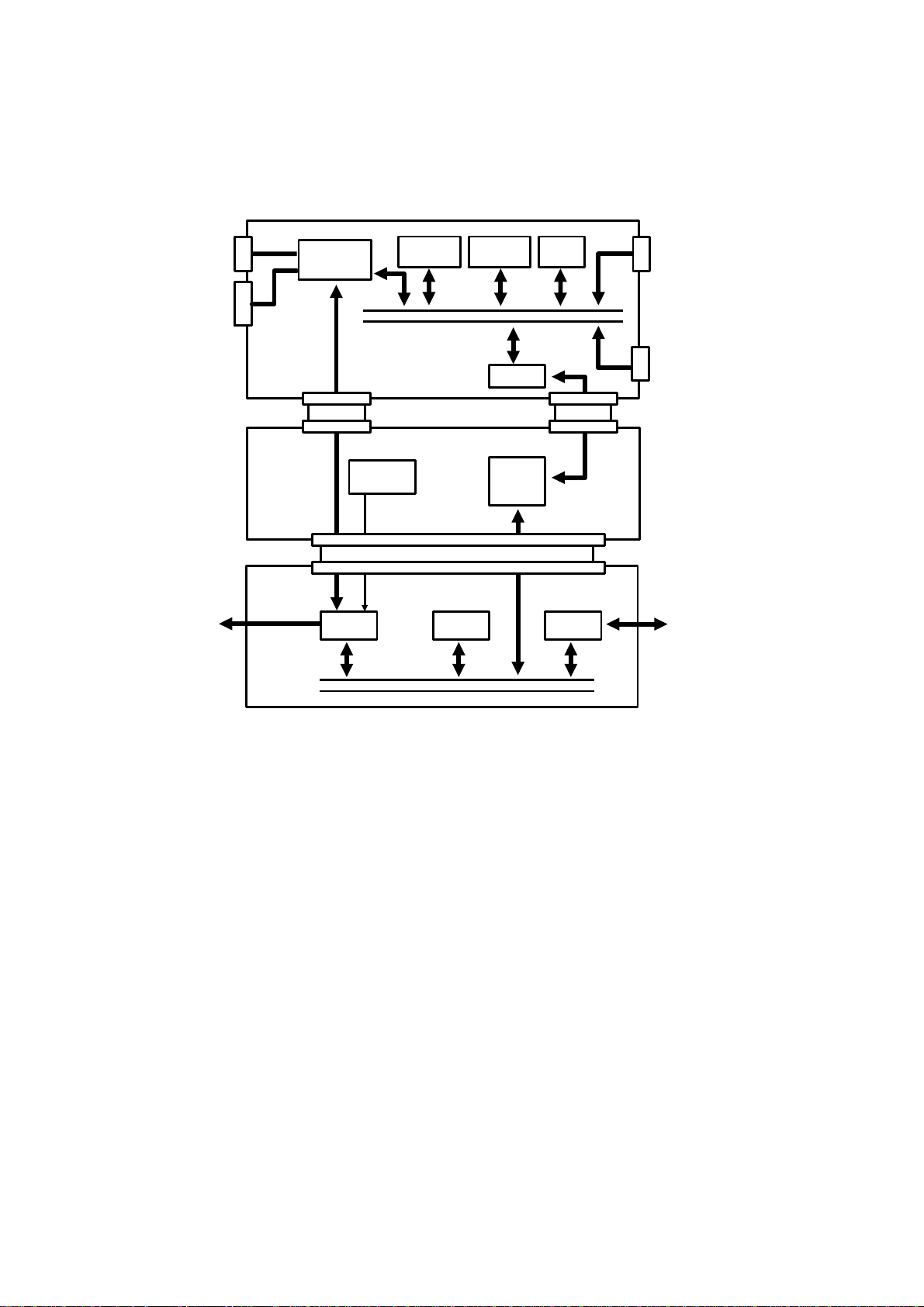
1.2. OVERALL SYSTEM CONTROL
Serial I/F
Parallel I/F
To Printer
Mechanism
Printer Data I/F
Interface
Controller
LIF
Memory
Controller
Oscillator
24.1 MHz
ADDRESS/DATA BUS
Page
Optional
Memory
ADDRESS/DATA BUS
PIF
FCU
CPU
CPU
CPU
Font
ROM
LIOP
IC Card
Font Cartridge
LCD/LED Data
To/ From
Operation Panel
The printer interface kit consists of two PCB s, th e printe r cont rolle r board
(Controller) and the printer interface board (PIF).
1.2.1. Printer Data Path
Through the serial and/or parallel interfa ce(s), the Cont rolle r han dsh ake s wit h
the host(s) and receives print data, using one of the available emulation
modes. Then the CPU creates an imaginary page in the memory using the
fonts stored in the font ROM a nd th e f on t ca rtridge. After one page of print
data has been created, the Controller sends the video data through the video
interface to the LIF on the FCU for print ing . The PIF supplies the 24.1 MHz
clock signal to the LIF for 300 dpi printing.
1-2
Page 5
Aug. 11, 1993 OVERALL INFORMATION
POWER DISTRIBUTION
1.2.2. LCD/LED Data Path
The three LEDs on the operation panel are always dedicated to the Controller. They indicate the status during printing, and are directly co nt rolled by the
Controller.
In Printer Mode (Function 35), the LCD display and four one-touch dial keys
are dedicated to the Controller to access SelecTyp e functions. Within the SelecType functions, some settings are not ava ilable because of limitations to
the machine’s hardware. So, the CPU on the PIF monitors the functio n sta tus
and the settings to indicat e on the LCD, and mod ifies the data if necessary
(e.g., Half Letter size paper will not be displayed as a possible paper size ).
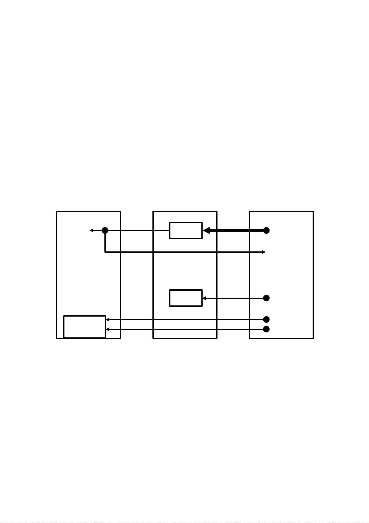
1.3. POWER DISTRIBUTI O N
Controller PIF FCU
To ICs
+5VD
DC/DC +24VS
+5VDMON
CPU +5V
+12V
Serial I/F
-12V
The PIF generates +5VD for the Controller. The +5VD line is returned to the
FCU as +5VDMON, so that the FCU can detect whether the printer inte rfa ce
is installed or not.
+5V for the PIF CPU, and ± 12V for the serial interfa ce on the Controlle r are
directly supplied by th e FCU.
1-3
Page 6
Aug 11th, 1993 DETAILED SECTION DESCRIPTIONS
INTERFACE SPECIFICATIONS
2. DETAILED SECTION DESCRIPTIONS
2.1. INTERFACE SPECIFICATIONS
2.1.1. Parallel Interface
1. Pin Assignments
The printer has an 8-bit parallel int erf ace. The pin assignments are as follows.
Signal
Pin
119
2 - 9 20 - 27 DATA1-8 IN Parallel data bits 1 to 8. A HIGH represents a ’1’.
10 28
11 29 BUSY OUT
12 30 PE OUT A HIGH indicates that the printer is out of paper.
13 - SLCOUT OUT Pulled up to 5 V through a 3.3 kΩ resistance.
14 -
16 - GND - Logic ground
17 - CH-GND - Printer’s chassis ground
19 - 30 - GND - Twisted pair return signal ground level
31 -
32 33 - GND - Logical ground
35 - + 5V - Pulled up to 5 V through a 3.3 kΩ resistance.
36 -
Return
Pin
Signal
STROBE IN
ACKNLG OUT
Autofeed IN
INIT IN
ERROR OUT
SLCIN in
Direct-
ion
Description
The strobe pulse from the host to read data in.
The received pulse width must be more than 0.5
µs. Normally HIGH; data reception starts when
the signal goes LOW.
A 10 µs pulse. LOW indicates that data has been
received and the printer is ready to receive more
data. This signal is output as a pair with BUSY.
A HIGH indicates that the printer cannot receive
data. The signal is high when data is entering,
when the printer is off line, and when there is a
printer error.
When LOW, paper is automatically fed when CR
is received (the active signal level can be
selected by a user adjustment). Sampling is
carried out when power is on or when the printer
is initialized at the operation panel.
When this goes low, the printer controller ignores
the STROBE signal.
This becomes low when the printer is out of
paper, off line, or in an error condition.
The DC1/DC3 control codes are valid only when
this signal is HIGH (SLCIN is OFF). This setting
can be changed with a user adjustment.
Sampling is only done when the power is on.
Pins 15, 18, and 34 are no t use d.
2-1
Page 7
DETAILED SECTION DESCRIPTIONS Aug 11th, 1993
INTERFACE SPECIFICATIONS
Notes: • All interface conditions are based on TTL level. Both the rise and
fall of each signal must be less than 0. 2 µs.
• Data transfer must be carried out by observing the ACKNLG or
BUSY signal. (Data transfer to the printer can be carried out only
after the receipt of the ACKNLG signal or when BUSY is LOW.)
• The "Direction" column refers to the direction of sign al flo w as
viewed from the printer.
• "Return Pin" denotes the twisted-pair return to be conn ect ed at sig-
nal ground level. For the int erf ace wirin g, a twiste d-p air cable
should be used for each signal an d the connection should be completed on the return side. These cables should be shielded and
connected to th e cha ssis o f th e ho st computer and the printer.
2. Interface Timing
The following diagram shows the timing for the parallel interface.
AB
DATA 1-8
VALID VALID
A
STROBE
C
BUSY
ACKNLG
A: 0.2 microseconds minimum
B: 0.1 microseconds minimum
C: 0.15 microseconds maximum (normally 0.12)
D: 0.3 microseconds minimum (normally 0.5)
E: 0.07 microseconds maximum (normally 0.03)
F: 1 to 2 microseconds (normally 1.7)
G: Always at least zero
Signal Level: TTL Compatible
G
D
E
F
2-2
Page 8

Aug 11th, 1993 DETAILED SECTION DESCRIPTIONS
INTERFACE SPECIFICATIONS
2.1.2. Serial Interface
1. Data Format
Word Length: 7 or 8 bits
Parity: None, odd, or even
Stop Bits: 1 or 2
Printer Ready Protocol: Enabled (DTR and XON/XOFF protocol set to ON)
The data format settings can be adjusted by user level features.
Baud Rate: 300, 600, 1200, 2400, 4800, 96 00, 19200 bps
Signal Level: RS-2 32C; conforms to EIA
Connector: D-sub 25-pin connector
2. Pin Assignments
The serial interface pin assign ments are described below. The d irect ion of the
signal is given relative to the prin te r.
Signal
Pin
1 FG - Connected to the printer chassis.
2 TXD OUT Serial data from printer to computer.
3 RXD IN Serial data from computer to printer.
4 RTS OUT Request To Send. Held HIGH by the printer.
5CTSIN
6 DSR IN
7 SG - Signal Ground. Provides a ground for all signal lines.
20 DTR OUT
Signal
Direct-
ion
Description
Clear To Send. The computer is ready to receive from
the printer. The printer will not proceed unless the
signal is HIGH. The active signal level can be changed
with a user adjustment.
Data Set Ready. The computer is ready to receive from
the printer. The active signal level can be changed with
a user adjustment.
Data Terminal Ready. Indicates whether the printer is
ready to receive data. If the printer ready protocol is not
selected, DTR is always HIGH (always ready to
receive). If printer ready protocol is selected, the printer
can only accept data when DTR is HIGH. When DTR
goes LOW, the computer must stop sending data within
128 characters. The active signal level can be changed
with a user adjustment.
2-3
Page 9

DETAILED SECTION DESCRIPTIONS Aug 11th, 1993
INTERFACE SPECIFICATIONS
3. Handshaking
The serial interface can use DTR signal le vels and XON/XOFF communication protocols either separately or in combination.
XON/XOFF Protocol
When the vacant area for data in the input buffer drops to 128 bytes, the
printer outputs an XOFF code, ind icating that the printer cannot receive more
data. Once the va can t area for data in the buffer recovers to 256 bytes, the
printer outputs an XON code, ind icating that the printer is again ready to receive data. XON/XOFF protocol can be selected with a user adjustment. The
factory setting is ENABLE D.
DTR/DSR Protocol
When the printer can receive data, the printer sets DTR to HIGH. When the
printer cannot receive data , it sets DTR to LOW. If the user’s DTR on/off adjustment is set to OFF, the DTR signal is always treated as HIGH. Th e p rint er
sends data on TXD only when DSR is HIGH, unless the user’s DSR on/of f adjustment is set to OFF, in which case the DSR signal is always treated as
HIGH.
2-4
Page 10

Aug 11th, 1993 DETAILED SECTION DESCRIPTIONS
INTERFACE SPECIFICATIONS
2.1.32.1.3. Printer Data Interface
1. 1. Signals
Name Description
VSREQ(X)
HSYNC(X) Clock signal to synchronize each line of image data.
VIDEO(X) Raster data for printing.
WCLK(X) Clock signal to synchronize raster data.
CPRDY(X) Inactive (high) when initializing or resetting the printer mechamism.
PRINT(X) Active (low) before transferring one page of image data to the FCU.
PRRDY(X)
CTBSY(X) Active (low) while the controller is sending a command to the FCU.
ETBSY(X) Active (low) while the FCU is sending status data to the controller.
CMD(X) Command data (8 bit serial).
STS(X) Status data (8 bit serial).
SRCLK(X) Clock signal to synchronize commands and status data.
Active (low) while the controller transfers one page of image data to the
FCU.
Active (low) while the printer mechanism is in standby status. Inactive
(high) while the printer is busy or has a problem.
Signal Directions
Controller PIF FCU
VSREQX
HSYNCX
VIDEOX
WCLKX
CPRDYX
PRINTX
PRRDYX
CTBSYX
ETBSYX
CMDX
STSX
SRCLKX
VSREQ
HSYNC
VIDEO
WCLK
CPRDY
PRINT
PRRDY
CTBSY
ETBSY
CMD
STS
SRCLK
Printer I/F Unit FAX Unit
2-5
Page 11

DETAILED SECTION DESCRIPTIONS Aug 11th, 1993
INTERFACE SPECIFICATIONS
2.2. Power-On Timing
CPRDY(X)
High
Low
Power On
Don’t
Care
1.5s (min.)
Communication
Impossible
0.5s
(min.)
2.5s (min.)
Initializing
Communication
Possible
When the power is switched on, the controller raises CPRDY(X) to high for
more than 0.5 s, then initializes it self with in 2 .5 s. A ft er in itializing is completed, the controller will be rea dy to commun icat e with the host PC(s) and
the FCU.
3.3. Reset Timing
CPRDY(X)
High
Low
Reset
0.5s (min.)
Communication
Impossible
2.5s (min.)
Initializing
Communication
Possible
When the user resets the prin ter using function 35, the controller activat es
CPRDY(X) for more than 0.5 s, then the controller initia lizes itself and the
printing process is canceled . A ft er initializing is completed, the controller will
be ready to communicate with the host PC(s) and the FCU.
2-6
Page 12

Aug 11th, 1993 DETAILED SECTION DESCRIPTIONS
INTERFACE SPECIFICATIONS
4.4. Image Data Synchronization (Horizontal)
HSYNC(X)
H
L
8 x WCLK(X)
VIDEO(X)
H
L
1 line of print data
8 x WCLK(X)
2550 x WCLK(X)
WCLK(X)
H
L
The FCU drops HSYNC(X) to low for eight WCLK(X) clock cycles befo re receiving each line of image data. Then, after the next eight cycles of WCLK(X)
has passed, the contro ller starts to transfer one line of image data.
The frequency of the WCLK(X) clock is between 1.3 MHz and 1.96 MHz.
HSYNC(X)
H
L
VIDEO(X)
1/4 inch
(6.4 mm)
Printable Area
1/4 inch
(6.4 mm)
2-7
Page 13

DETAILED SECTION DESCRIPTIONS Aug 11th, 1993
INTERFACE SPECIFICATIONS
5.5. Image Data Synchronization (Vertical)
PRINT(X)
H
L
VSREQ(X)
T3
H
L
VIDEO(X)
H
1st Page 2nd Page
L
T1 T2
PRINT(X)
Monitor Timing
The FCU monitors the PRINT(X) sign al fro m t he controller every 2 ms to detect if a print reque st is co ming from the controller or not. After T1 ha s passed
since the FCU detected the PRINT(X) signal to be active, the FCU drop s
VSREQ(X) to low so that the controller can acknowledge that the printer is
ready to receive one page of image data. After one page of data h as b ee n re ceived from the controller, the FCU inactivates the VSREQ(X) signal until
PRINT(X) is activate d again for printing the next page.
The times T1, T2 and T3 vary depen ding on the following conditions.
Parameter Time Condition
T1
Parameter Paper Size Time
T2
T3
1.0 s When the hexagonal mirror motor is active.
6.0 s When the hexagonal mirror motor is inactive.
Letter 8.5 s
Legal 10.6 s
A4 9.0 s
Letter 7.58 s
Legal 9.64 s
A4 8.06 s
2-8
Page 14

Aug 11th, 1993 DETAILED SECTION DESCRIPTIONS
INTERFACE SPECIFICATIONS
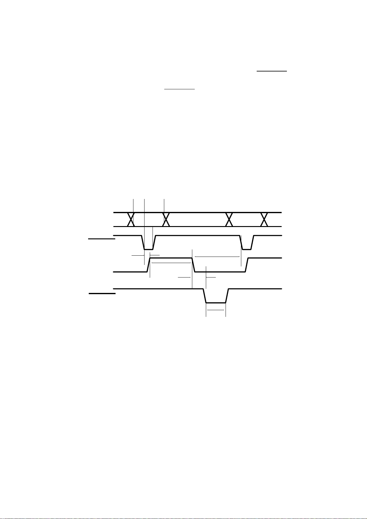
6.6. Command / Status Signal Timing
CTBSY(X)
ETBSY(X)
CMD(X)
STS(X)
SRCLK(X)
(153.6 kHz)
H
L
H
L
H
L
T3
T1
T2
T4 T5 T6
T7
STS informs the controller of stat us inf ormation, such as the current paper
size and any mechanical problems tha t are enco untered.
The FCU informs the controller of the printer status (STS ) in an 8 bit serial format, in response to a command (CMD) fro m the cont rolle r. If a status signal
(STS) is not received within T5 (100 ms) after the controller sends a command, the controller will resend the command to the FCU.
Refer to the above diagram and to the following table be low for t he timing .
Parameter Time
T1 62.7 µs
T2 Less than 30 ms
T3 9.77 µs
T4 4.07 µs
T5 Less than 100 ms
T6 9.77 - 10.58 µs
2-9
Page 15

Aug. 11, 1993 INSTALLATION
PRINTER INTERFACE UNIT
3. INSTALLATION
Throughout this chapter, the machine types are referred to as model codes H510 and H511.
This installation must only be done by qualified service personnel.
Note: The H510 does not have a monitor speaker.
Ignore the steps regarding the monitor speaker.
3.1. PRINTER INTERFACE UNIT
1. First, print any messages still stored in the SAF.
2. Turn off the power, and unplug the machine from the wall socket.
3. Slide out the cassettes.
4. Take off the rear cover [A] and disconnect the monitor speaker [B].
[A]
5. If a memory card [C] is installed, remove it.
[C]
[B]
3-1
Page 16

INSTALLATION Aug. 11, 1993
PRINTER INTERFACE UNIT
6. Take off the monitor speaker [D] from the rear cover.
7. Attach the monitor speaker [E] to the printer interface unit [F].
Then reconnect the monitor speaker [G].
[F]
[D]
[E]
3-2
[G]
Page 17

Aug. 11, 1993 INSTALLATION
PRINTER INTERFACE UNIT
8. Hold the printer interface unit [H] near the machine with one hand, and plug the flat cable
[ I ] into the connector on the FCU board.
[ I ]
[H]
9. Attach the printer interface unit [J].
[J]
3-3
Page 18

INSTALLATION Aug. 11, 1993
PRINTER INTERFACE UNIT
10. Remove the memory option cover [K].
1 1. Attach the memory card guide [L]. Then install the memory card if necessary.
[L]
[K]
Caution: To avoid damaging the memo ry card, always remove the mem-
ory card first before removing the printer interface unit.
12. Put back the memory option cover.
13. Put back the cassettes.
14. Plug in the machine, then turn on the power.
3-4
Page 19

[N]
[M]
Aug. 11, 1993 INSTALLATION
MEMORY EXPANSION BOARD (OPTIONAL)
3.2. MEMORY EXPANSION BOARD (OPTIONAL)
1. Print any messages still stored in the SAF.
2. Turn off the power and unplug the machine from the wall socket.
3. Remove the memory option cover [M] and the memory board cover [N].
4. Insert the memory expansion board [O].
5. Put back the memory board cover [P] and the memory option cover [Q].
6. Plug in the machine, then turn on the power.
[P]
[O]
[Q]
Caution:
Do not plug in or switch on until everything is connected up.
3-5
Page 20

Aug. 11, 1993 SERVICE TABLES AND PROCEDURES
SERVICE LEVEL FUNCTIONS
4.4. SERVICE TABLES AND PROCEDURES
4.1.4.1. SERVICE LE VE L FUNCTIONS
There are no special service operations. Refer to the operation manual for all
printer operation proced ure s.
4.2.4.2. SERVICE RAM ADDRESSES
4B8B
Data wait time after the last page has been printed, when print ing from th e
printer interface. (Hex; unit 2.56 s)
4-1
Page 21

Aug. 11, 1993 TROUBLESHOOTING
ERROR CODES
5. TROUBLESHOOTING
5.1. ERROR CODES
The following error messag es may appe ar on the screen while the printer interface is in operation.
Code Cause Required Action
C0002 Bus error Switch the printer off, wait a
C0003 Address error
C0004 Illegal instruction
C0005 Division by zero
C0006 CHK instruction executio n
C0007 TRAPV instruction execu tion
C0008 Privilege violation
C0009 Tr a ce mode execution
C0010 Implemented instruction
C0011 Implemented instruction
C0015 Unitialized interrupt
C0024 Spurious interrupt
C1110 ROM error (0 - 80 KH)
C1130 ROM error (100 - 180 KH)
C1140 ROM error (100 - 200 KH)
C1200 EEPROM write error
C1300 No ready task
C1310 Re-generation of existing task
C1400 Auto vector interrupt level 7
C9999 Undefined are a ema ncipation
few seconds, and switch back
on. If the error occurs again,
change the FCU or the printer
interface board.
5-1
Page 22

Aug. 11, 1993 PARTS CATALOG
PARTS LAYOUT
66. PARTS CATALOG
6.1. PARTS LAYOUT
100
1
100
3
2
101
13
101
12
14
101
5
100
6
7
8
3
4
11
10
101
101
9
102
10
6-1
Page 23

PARTS CATALOG Aug. 11, 1993
PARTS LIST
6.2. PARTS LIST
Index Part Number Description
1 H5105321 Flat Cable: PIF - FCU
2 H5106005 PCB: CNT: USA
3 H1443167 Stud - PIF
4 H5105610 PCB: PIF: USA
5 H5105320 Flat Cable: PIF-CNT: USA
6 G0111250 Screw: Con: NA: M
7 H1443168 Cover - Option Memory Board
9 H1444146 Guide - Option Memory Card
10 H0814141 Screw - Handset
11 H1444145 Rear Cover - Memory - PIF
12 H1444111 Rear Cover - Printer Option
13 H1444144 Cover - RS232C
14 H1444140 Cover - Left - PIF: USA
* H1444141 Cover - Cartridge
* H1444128 Spring - Cover Cartridge
100 09513006B Philips Screw with Flat Washer - M3 x 6
101 03530060Z Philips Truss Head Screw - M3 x 6
102 09513010B Philips Screw with Flat Washer - M3 x 10
* H1444301 Operator’s Manual
* 09653008B Tapping Screw - M3 x 6
6-2
 Loading...