®
RT9526A
Linear Single Cell Li-Ion Battery Charger with Input Over
Voltage Protection
General Description
The RT9526A is a fully integrated low cost single cell Liion battery charger ideal for portable applications. The
RT9526A is capa ble of being powered up from AC ada pter
and USB (U niversal Serial Bus) port inputs. The RT9526A
enters sleep mode when supplies are removed. The
RT9526A opti mizes the charging task by using a control
algorithm including preconditioning mode, fast charge
mode, and consta nt voltage mode. The charging ta sk will
remain in constant voltage mode to hold the battery in a
full charge condition. The charge current can be
programmed with a n external resistor . The internal thermal
feedback circuitry regulates the die temperature to opti mize
the charge rate under all ambient temperatures. The
RT9526A features 28V maximum rating voltage for VIN.
Under-voltage protection a nd over-voltage protection are
provided for the AC a da pter supply.
The RT9526A is available in the WDFN-8L 2x3 and
SOT-23-6 pa ckage to achieve be st solution for PCB space
and total BOM cost saving considerations.
Applications
Cellular Phones
Digital Camera s
PDAs and Smart Phones
Portable Instruments
Features
28V Maximum Rating for AC Adapter with Over-
Voltage Protection 7V
Internal Integrated Power FETs
AC Adapter Power Good Status Indicator
Programmed Charging Current
Charge Status Indicator
Programmed End of Charge Current
Under-Voltage Protection
Thermal Feedback Optimizing Charge Rate
RoHS Compliant and Halogen Free
Ordering Information
RT9526A
Package Type
QW : WDFN-8L 2x3 (W-Type)
E : SOT-23-6
Lead Plating System
G : Green (Halogen Free and Pb Free)
Note :
Richtek products are :
RoHS compliant and compatible with the current require-
ments of IPC/JEDEC J-STD-020.
Suitable for use in SnPb or Pb-free soldering processes.
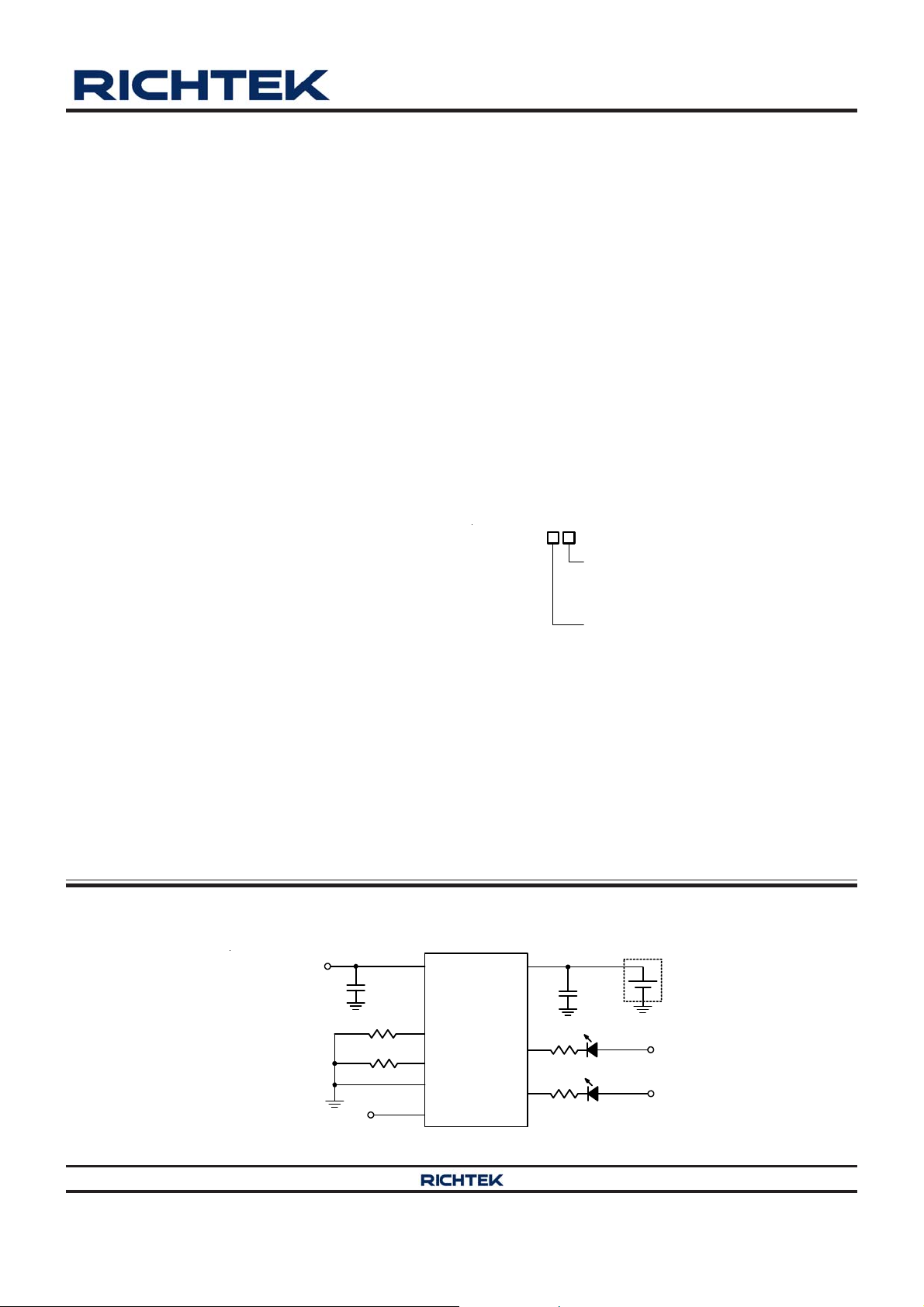
Simplified Application Circuit
Adapter or USB
C
IN
R
ISET
R
IMIN
Copyright 2014 Richtek Technology Corporation. All rights reserved. is a registered trademark of Richtek Technology Corporation.
©
DS9526A-03 July 2014 www.richtek.com
VIN
ISET
IMIN
GND
ENB
RT9526A
CHG_SB
BATT
PGB
R1
R2
C
OUT
V
BATT
V
BATT
1
RT9526A
Marking Information
RT9526AGQW
05 : Product Code
05W
RT9526AGE
0X=DNN
W : Date Code
0X= : Product Code
DNN : Date Code
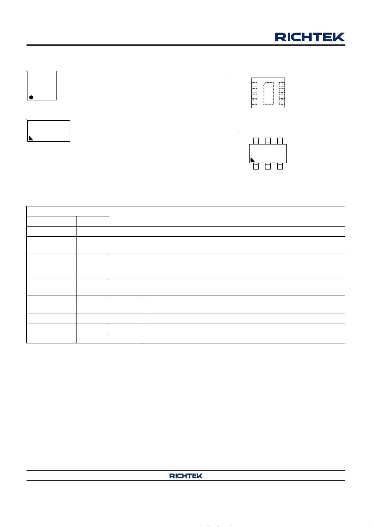
Function Pin Description
Pin No.
WDFN-8L 2x3 SO T-2 3- 6
1 3 VIN Supply Voltage Input. VIN can withstand up to 28V input.
2 -- PGB
3 1 CHG_SB
4 -- ENB
5,
9 (Exp ose d Pad)
2 GND
6 6 IMIN EOC Current Setting.
7 5 ISET Charge Current Set Point.
8 4 BATT Battery Charge Current Output.
Pin Name Pin Fun ction
Pin Configurations
(TOP VIEW)
1
VIN
2
PGB
CHG_SB
3
4
ENB
WDFN-8L 2x3
IMIN
CHG_SB
SOT-23-6
Po wer Go od In dic ato r . This pin con nec ts to VIN with 10S L N-M O SFE T
as power good condition.
Charge Status Indicator Output (Open-Drain). Indicate low when
bat t ery is charging; indi c ate hi gh wh en ba tte r y char gi ng fi nish ed or an y
fault happened.
Enable Control Input (Active Low). Connect this pin with a 200k
pull-low resistor.
Ground. The exposed pad must be soldered to a large PCB and
connected to GND for maximum power dissipation.
8
7
6
GND
9
5
ISET BATT
4
56
23
VIN
GND
BATT
ISET
IMIN
GND
Copyright 2014 Richtek Technology Corporation. All rights reserved. is a registered trademark of Richtek Technology Corporation.
2
©
DS9526A-03 July 2014www.richtek.com
Function Block Diagram
RT9526A
Switch
Well
Operation
VIN
ISET
ENB
BASE
Sleep
Mode
Current
Set Block
OVP
UVLO
200k
V
I
BIAS
REF
CC/CV/TR
Multi Loop
Controller
Logic
EOC Set
Block
BATT
IMIN
CHG_SB
PGB
GND
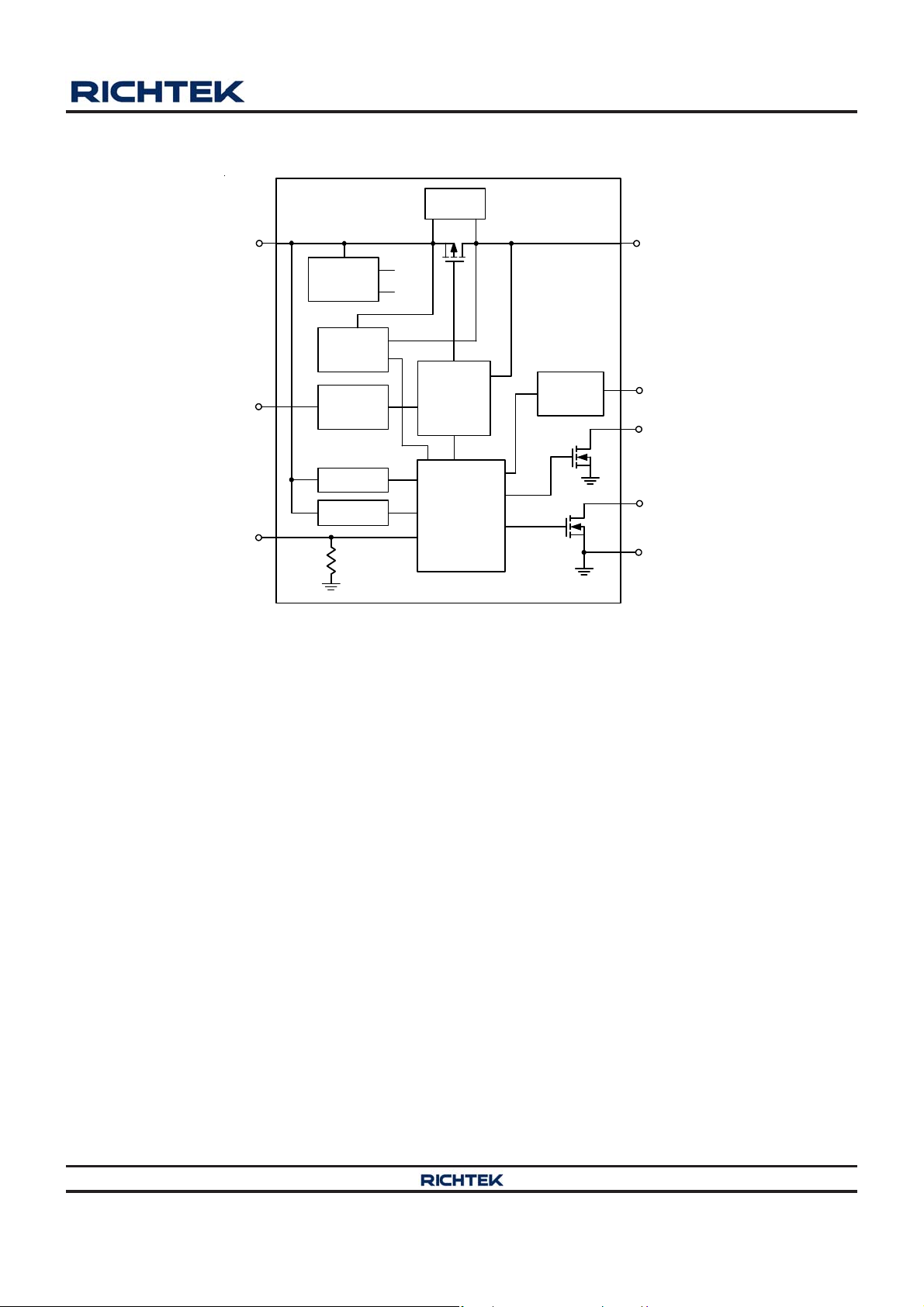
The RT9526A is a fully integrated low cost single cell Liion charger. It provides a fast-charge current setting by
resistor R
. Pre-charge is 16.7% of fast charge current,
IREF
while VBAT < 2.45V. The PGB pin is low, while VIN >
POR, VIN < OVP , and VIN − VBA T > V
. The CHG_SB
OSH_H
pin is low, while RT9526A is charging. The CHG_SB pin
will go high while end of charger happen s. End of charge
condition is set by R
. CHG_SB will go low again, while
IMIN
charge current is larger than 75% of fast-charge setting.
The RT9526A charges continuously after end of charge
happen s. Li-ion battery will be full charged until CV = 4.2V .
The RT9526A ca n be disa bled by ENB = H.
Copyright 2014 Richtek Technology Corporation. All rights reserved. is a registered trademark of Richtek Technology Corporation.
©
DS9526A-03 July 2014 www.richtek.com
3
RT9526A
Absolute Maximum Ratings (Note 1)
Supply V oltage, VIN ------------------------------------------------------------------------------------------------------ −0.3V to 28V
CHG_SB, PGB ------------------------------------------------------------------------------------------------------------ −0.3V to 7V
Other Pins------------------------------------------------------------------------------------------------------------------- −0.3V to 6V
Power Dissipation, P
WDFN-8L 2x3 -------------------------------------------------------------------------------------------------------------- 3.17W
SOT-23-6 -------------------------------------------------------------------------------------------------------------------- 0.48W
Package Thermal Re sistance (Note 2)
W DF N-8L 2x3, θJA--------------------------------------------------------------------------------------------------------- 31.5°C/W
WDFN-8L 2x3, θJC--------------------------------------------------------------------------------------------------------- 7.5°C/W
SOT-23-6, θJA--------------------------------------------------------------------------------------------------------------- 208.2°C/W
Lead Temperature (Soldering, 10 sec.)------------------------------------------------------------------------------- 260°C
Junction T emperature----------------------------------------------------------------------------------------------------- 150°C
Storage T emperature Range -------------------------------------------------------------------------------------------- −65°C to 150°C
Recommended Operating Conditions (Note 3)
Junction T emperature Range-------------------------------------------------------------------------------------------- −40°C to 125°C
Ambient T emperature Range-------------------------------------------------------------------------------------------- −40°C to 85°C
@ T
D
= 25°C
A
Electrical Characteristics
(V
= 4.5V, T
IN
VI N POR Ri si ng Thresh old
Voltage
VIN POR Falling Threshold
Voltage
VIN V
VIN V
VI N Standby Cur rent V
BATT Sleep Leakage Current I
Battery Regulation Voltage V
VIN Power M OSFET
On-Resistance
IS ET Set Volta ge
(Fast Charge Phase)
Cha r ge Cur ren t Acc urac y R
BATT Pre- Cha r ge Thr es hol d V
BATT Pre- Cha r ge Thr es hol d
Hysteresis
Pre-Charge Current I
ENB Input
T hres hol d Vol tag e
Th erm al R egu lati on T
= 25°C unless otherwise specified)
A
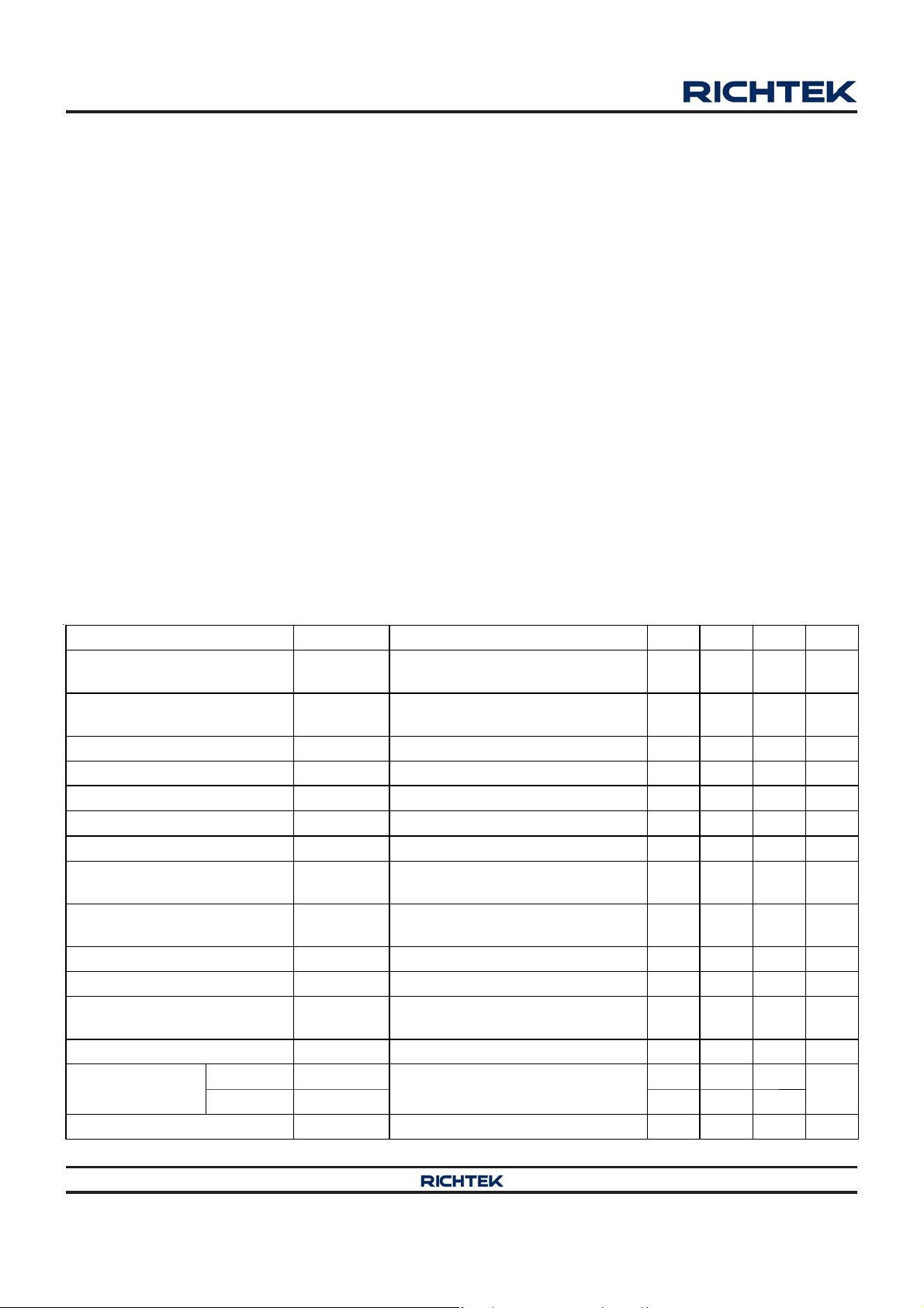
Parameter Symbol Test Conditions Min Typ Max Unit
VOS Rising V
BATT
VOS Fa llin g V
BATT
Logic-High V
V
V
SLEEP
R
V
V
CHG_PRE
3.4 3.8 4.2 V
POR_H
3.1 3.5 3.9 V
POR_L
-- 90 150 mV
OS_H
10 50 -- mV
OS_L
-- 1 5 A
4.158 4.2 4.242 V
REG
I
DS(ON)
-- 1.22 -- V
ISET
CHG_PRE
CHG_PRE
2.45 2.55 2.65 V
40 100 150 mV
12 16.7 21.3 %
IH
Logic-Low VIL -- -- 0.4
-- 115 -- C
REG
= 4.5V -- 400 600 A
BATT
= 0.5A -- 0.6 --
BATT
= 24.3k 450 500 550 mA
ISET
= 4.2V to 24V
V
IN
1.5 -- -V
Copyright 2014 Richtek Technology Corporation. All rights reserved. is a registered trademark of Richtek Technology Corporation.
4
©
DS9526A-03 July 2014www.richtek.com
RT9526A
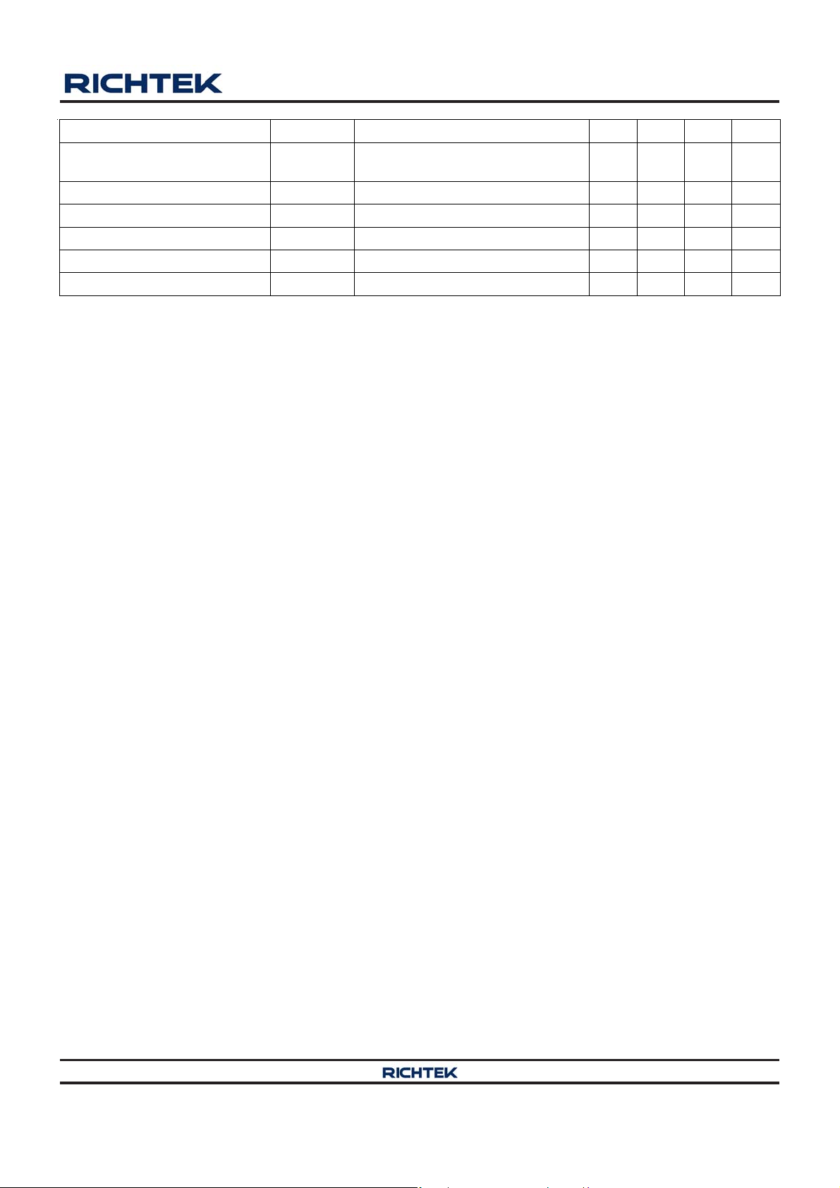
Parameter Symbol Test Conditions Min Typ Max Unit
VIN Over-Voltage Protection
Threshold
VIN OVP Hysteresis V
PGB Pull-Down Voltage 5mA -- 200 -- mV
CHG_SB Pull-Down Voltage 5mA -- 200 -- mV
EOC Current Setting I
EOC Rising Threshold R
Note 1. Stresses beyond those listed “Absolute Maximum Ratings” may cause permanent damage to the device. These are
stress ratings only, and functional operation of the device at these or any other conditions beyond those indicated in
the operational sections of the specifications is not implied. Exposure to absolute maximum rating conditions may
affect device reliability.
Note 2. θ
Note 3. The device is not guaranteed to function outside its operating conditions.
is measured at T
JA
measured at the exposed pad of the package.
A
V
6.7 7 7.5 V
OVP
-- 0.1 -- V
OVP
R
IMIN
= 25°C on a high effective thermal conductivity four-layer test board per JEDEC 51-7. θJC is
= 243k -- 45 -- mA
IMIN
= 24.3k 337.5 375 412.5 mA
IREF
Copyright 2014 Richtek Technology Corporation. All rights reserved. is a registered trademark of Richtek Technology Corporation.
DS9526A-03 July 2014 www.richtek.com
©
5
 Loading...