

RT9701
100mΩΩΩΩ Power Distribution Switches
General Description
The RT9701 is an integrated 100mΩ power switch
for self-powered and bus-powered Universal Series
Bus (USB) applications. A built-in charge pump is
used to drive the N-channel NMOSFET that is free
of parasitic body diode to eliminate any reversed
current flow across the switch when it is powered
off. Its low quiescent supply current (23µA) and
small package (SOT-25) is particularly suitable in
battery-powered portable equipment.
Several protection functions include soft start to limit
inrush current during plug-in, current limiting at 1.5A
to meet USB power requirement, and thermal
shutdown to protect damage under over current
conditions.
Applications
Battery-Powered Equipment
z
Motherboard USB Power Switch
z
USB Device Power Switch
z
Hot-Plug Power Supplies
z
Battery-Charger Circuits
z
Ordering Information
Features
z
100mΩΩΩΩ Typ. High-Side NMOSFET (SOT- 25)
Guaranteed 1.1A Continuous Current
z
1.5A Current Limit
z
Small SOT- 25 Package Minimizes Board Space
z
Soft Start
z
Thermal Protection
z
Low 23µµµµA Supply Current
z
Wide Input Voltage Range: 2.2V ~ 6V
z
UL Approved - #E219878
z
Pin Configurations
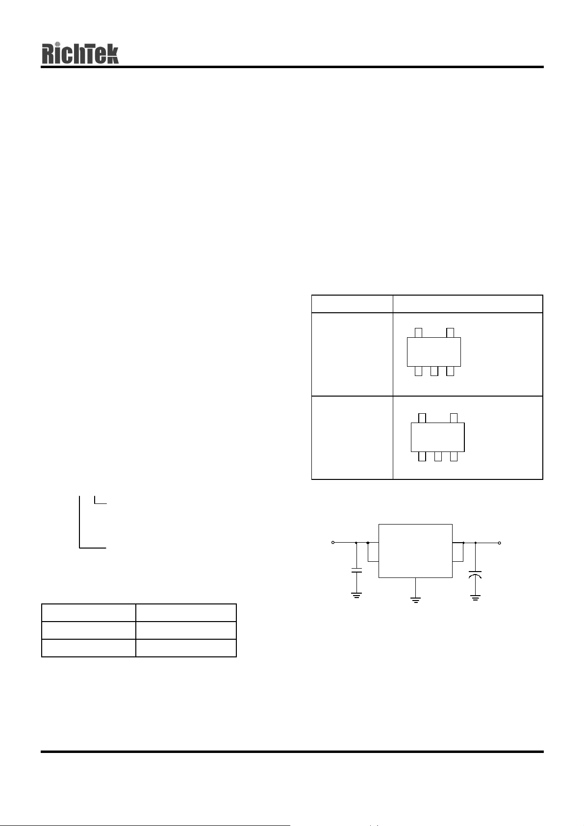
Part Number Pin Configurations
RT9701CBL
(Plastic SOT-25)
RT9701CB
(Plastic SOT-25)
54
321
54
321
TOP VIEW
1. VOUT
2. GND
3. VIN
4. VIN
5. VOUT
TOP VIEW
1. VOUT
2. GND
3. VIN
4. CE
5. VOUT
RT9701
Package type
Typical Application Circuit
BL : SOT-25
B : SOT-25
Operating temperature range
C: Commercial standard
IN
C
IN
1 µF
RT9 701 CBL
VINV
VIN
GND
VOUT
VOUT
*C
OUT
470 µF
V
OUT
Marking Information
Part Number Marking
RT9701CBL AH
RT9701CB C0
DS9701-05 October 2001 www.richtek-ic.com.tw
* 470µF, Lo w ESR Electro lyti c
1
RT9701
Pin Description
Pin Name Pin Function
VIN Power Input
VOUT Output Voltage
GND Ground
CE Chip Enable
Test Circuits
C
IN
V
IN
+
V
IN
Switch Off
V
OUT
RT9701 CBL
VIN
VIN
VOUT
VOUT
GND
I
OUT
+
C
L
I
R
L
L
Test Circuit 1
V
IN- SW
RT9701 CBL
VIN
VOUT
VOUTVIN
+
C
IN
GND
C
L
V
OUT
+
R
L
Test Circuit 2
V
IN
RT9701 CB
VIN
CE
V
+
C
IN
CE
VOUT
VOUT
GND
I
OUT
C
L
V
OUT
+
I
R
L
L
On
Off
Test Circuit 3
Test Circuit 2 is performed by charging an external tank of bulk capacitor to the input then applying this voltage to
the input of the unit.
All typical operating characteristics curves showed are referred to Test Circuit 1, unless specified to Test Circuit 2
or Test Circuit 3.
www.richtek-ic.com.tw DS9701-05 October 2001
2

Function Block Diagram
RT9701
CE
Bias
Charg e
Pump
Oscillator
Control
Thermal
Detection
Current
Limit
RS
NMOSFE T
VIN
(VIN)
(VOUT)
VOUT
GND
Absolute Maximum Ratings
z Supply Voltage 7V
z Chip Enable -0.3V ~ 7V
z Power Dissipation, P
SOT-25 0.25W
z Operating Junction Temperature Range -20°C ~ 100°C
z Storage Temperature Range -65°C ~ 150°C
z Package Thermal Resistance
SOT-25, θ
z V
OUT
JA
ESD Level
HBM (Human Body Mode) 8KV
MM (Machine Mode) 800V
@ TA = 25°C
D
250°C /W
DS9701-05 October 2001 www.richtek-ic.com.tw
3
RT9701
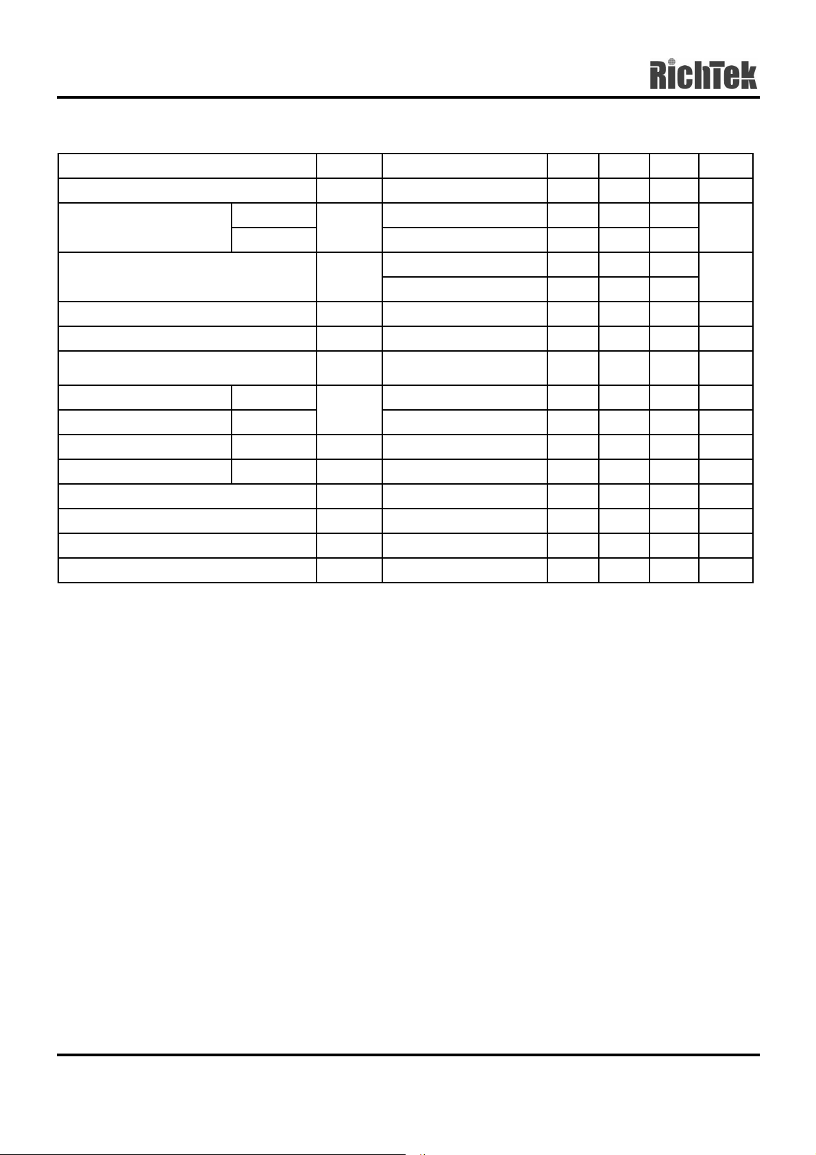
Electrical Characteristics
(V
= 5V, CIN = C
IN
= 1µF, TA = 25°C, unless otherwise specified)
OUT
Parameter Symbol Test Conditions Min Typ Max Units
Input Voltage Range
V
IN
2.2 -- 6 V
RT9701CBL IL = 1A -- 100 130
Output NMOFET R
DS(ON)
RT9701CB
R
DS(ON)
IL = 1A -- 105 135
mΩ
VIN = 3V -- 19 40
Supply Current
Output Turn-On Rising Time
Current Limit Threshold
Short-circuit Fold Back Current
T
R
I
LIMIT
I
OS
V
= 5V
IN
RL = 10Ω, 90% Settling
RL = 2Ω
V
= 0V, measured
OUT
prior to thermal shutdown
--
--
23 45
400 --
1.1 1.5 2 A
-- 1.0 -- A
µA
µS
CE Input High Threshold RT9701CB 2.0 -- -- V
CE Input Low Threshold RT9701CB -- -- 0.8 V
Shutdown Supply Current RT9701CB
Output Leakage Current RT9701CB
VIN Under Voltage Lockout
VIN Under Voltage Hysteresis
Thermal Limit
Thermal Limit Hysteresis
I
OFF
I
LEAKAGE
UVLO 1.3 1.8 -- V
T
SD
∆T
SD
CE = “0” -- 0.1 1
CE = “0”, V
= 0V -- 0.5 10
OUT
-- 100 -- mV
-- 130 --
-- 20 --
µA
µA
°C
°C
www.richtek-ic.com.tw DS9701-05 October 2001
4

Typical Operating Charateristics
RT9701
40
VIN = 5V
35
30
µ
25
20
15
10
Quiessent Current ( µ A)
5
0
-40 -20 0 20 40 60 80 100 120
Temperature (ºC)
On-Resistance vs. Temp.
Supply Current vs. Temp.
160
140
)
120
Ω
100
80
60
40
On-Resistance (m )
20
0
-40-20 0 20406080100120
RT9701CBL
Temperature ( C)
VIN = 5V
RT9701CB
°C)
Supply Current vs. Voltage
40
T
35
30
µ
25
20
15
10
Quiescent Current (µ A)
5
0
2.0 2.5 3.0 3.5 4.0 4.5 5.0 5.5 6.0
VIN Voltage (V)
Voltage (V)
Ta = 25
On-Resistance vs. Voltage
160
140
120
)
Ω
100
80
60
40
On-Resistance (mOhm)
20
0
2.0 2.5 3.0 3.5 4.0 4.5 5.0 5.5 6.0
Voltage (V)
VIN Voltage (V)
Ta = 25
TA = 25°C
RT9701CBL
RT9701CBL
C
°
A
C
°
Current Limit vs. Temp.
2.20
2.00
1.80
1.60
1.40
1.20
Current Limit (A)
1.00
0.80
0.60
-40 -20 0 20 40 60 80 100 120
Temperature ( C)
°C)
VIN = 5V
1.80
1.58
1.35
1.13
0.90
0.68
Current Limit (A)
0.45
0.23
0.00
2.0 2.5 3.0 3.5 4.0 4.5 5.0 5.5 6.0
Current Limit vs. Voltage
TA = 25°C
Voltage (V)
VIN Voltage (V)
DS9701-05 October 2001 www.richtek-ic.com.tw
5

RT9701
µ
Short Circuit Current vs. Temp.
1400
1300
1200
1100
1000
900
800
700
Short Circuit Current (mA)
600
500
-40 -20 0 20 40 60 80 100 120
Temperature ( C)
°
°C)
CE Threshold vs. Temp.
2.4
2.0
1.6
1.2
VIN = 5V
VIN = 5V
Rising
Falling
Short Circuit Current vs. Voltage
1950
1700
1450
1200
950
700
Short Circuit Current (mA)
450
200
2.0 2.5 3.0 3.5 4.0 4.5 5.0 5.5 6.0
Voltage (V )
VIN Voltage (V)
Ta = 25
T
CE Threshold vs. Voltage
2.4
2.0
1.6
1.2
C
°
A
Rising
Falling
0.8
CE Threshold (V)
0.4
0.0
-40 -20 0 20 40 60 80 100 120
Temperature (ºC)
*Test Circuit 3
Turn On Rising Tim e vs. Temp.
720
630
µS)
µ S)
(
540
450
360
270
180
Turn-On Ris ing Time
90
0
-40 -20 0 20 40 60 80 100 120
Temperature (
RL = 30
CL = 1
°C)
Ω
F Ceramic
µ
*Test Circuit 3
VIN = 5V
0.8
CE Threshold (V)
0.4
TA = 25
0.0
2.0 2.5 3.0 3.5 4.0 4.5 5.0 5.5 6.0
Voltage (V)
VIN Voltage (V)
*Test Circuit 3
Turn Off Falling Time vs. Temp.
140
120
µ
100
80
60
40
Turn-Off Falling Time (µS)
20
RL = 30
CL = 1
0
-40 -20 0 20 40 60 80 100 120
Temperature (° C)
Ω
F Ceramic
*Test Circuit 3
°C
VIN = 5V
www.richtek-ic.com.tw DS9701-05 October 2001
6

RT9701
>
>
>
>
>
>
>
)
>
>
>2 >
>
>
>
>
>2 >
>
>3 >
>
>
Shutdown Supply Current vs. Temp.
0.9
0.8
µ
0.6
0.5
0.3
0.2
Turn-Off Supply Current (µ A)
0.0
-40 -20 0 20 40 60 80 100 120
Temperature (
°C)
*Test Circuit 3
UVLO Threshold vs. Temp.
3.50
3.00
2.50
2.00
VIN = 5V
VIN = 5V
Turn-Off Leakage Current vs. Tem p.
3.5
3.0
µ
2.5
2.0
1.5
1.0
0.5
Turn-Off Leakage Current (µ A)
0.0
-40 -20 0 20 40 60 80 100 120
Temperature (
°C)
*Test Circuit 3
Inrush Current Response
CL = 100µF
CL = 33µF
VIN = 5V
1.50
1.00
UVLO Threshold (V)
0.50
0.00
-40 -20 0 20 40 60 80 100 120
Temperature (
°C)
Turn-On Response
CH1
CH2
1
1
1 >1
2
2 >2
CH1: V
CH2: V
T
T
: 5V/Div
CE
: 1V/Div
OUT
Time (100µS/Div)
RL = 30 Ω, CL = 1µF
*Test Circuit 3
CH1
CH2
CH3
2
2 >3
3 >4
4
2 >2
3 >3
4 >4
I
IL = 1A/Div
OUT
1
1
1 >1
2
2 >2
CH1: V
3
3 >3
CH2: I
CL = 1µF
T
T
T
=1A/Div
Time (100µS/Div
100µS/Div
Turn-Off Response
T
T
T
: 5V/Div
CE
: 100mA/Div; CH3: V
OUT
Time (50µS/Div)
VIN = 5V, RL = 1 ohm
RL = 1Ω, VIN = 5V
RL = 30 Ω, CL = 1µF
: 2V/Div
OUT
*Test Circuit 3
DS9701-05 October 2001 www.richtek-ic.com.tw
7

RT9701
>
>
>2 >
>
>
g
g
>
>
>2 >
>
>
>
>
>2 >
>
>
>
>
>
>
>
>2 >
>
>
T
T
>
>
>
>
CH1
CH2
CH1
UVLO at Risin
1
1
1 >1
2
2 >2
T
CH1: V
T
CH2: V
RL = 30 Ω, CL = 1µF
Time (500µS/Div)
Inrush Short Circuit Response
T
V
=1.2V, depend on CIN ESR
DROP
I
: depend on ESR & ESL
1
1
1 >1
PEAK
: 1V/Div
IN
: 1V/Div
OUT
CH1
CH2
CH1
UVLO at Fallin
T
T
1
1
1 >1
CH1: V
2
2 >2
CH2: V
: 1V/Div
IN
: 1V/Div
OUT
Time (10mS/Div)
RL = 30 Ω, CL = 1µF
*Test Circuit 2
Soft-start Short Circuit Response
1
1
1 >1
T
CH2
CH1
CH2
2
2 >2
V
1
1
1 >1
2
2 >2
CH2: I
T
CH1 : VIN : 2V/Div
CH2 : I
C
= 1µF
IN
C
= 1000µF
L
25µS/Div
Ramped Load Response
OUT
= 5V
: 500mA/Div
OUT
4.9V
Current Limit Threshold
1mS/Div
: 10A/Div
L
V
= 4.6V
OUT
1.1A
VIN = 5V, CL = 1µF
CH1
CH2
CH2
2 >
2 >
2 >2 >
1
1 >
1 >1
2 >
2
2 >2
CH2: I
T
CH1 : VIN : 2V/Div
CH2 : I
C
IN
50µS/Div
Current Limit Response
Loading trigger
VIN = 5V, CL = 0.1µF
: 1A/Div
I
: 1A/Div
LOAD
OUT
RL = 1 ohm
5µS/Div
OUT
= 1µF
Ω
: 1A/Div
www.richtek-ic.com.tw DS9701-05 October 2001
8

>
>
>
Thermal Shut Down Response
T
1 >
1 >
CH
1
1 >1 >
CH3
Thermal Shut Down
T
2
2
2 >2
CH2
CH1: VCE : 5V/Div
CH3: I
CH2: I
OUT@RL
OUT
Ω : 1A/Div
1ohm : 500mA/Div
@short : 500mA/Div
Time (50mS/Div)
1A/Div
1A/Div
50mS/Div
VIN = 5V
Functional Description
The RT9701 is a high-side single N-channel switch
with active-high enable input.
Input and Output
VIN (input) is the power supply connection to the
circuitry and the drain of the output MOSFET. VOUT
(output) is the source of the output MOSFET. In a
typical circuit, current flows through the switch from
VIN to VOUT toward the load. Both VOUT pins must
be short on the board and connected to the load and
so do both VIN pins but connected to the power
source.
RT9701
Current Limiting and Short Protection
The current limit circuit is designed to protect the
system supply, the MOSFET switch and the load
from damage caused by excessive currents. The
current limit threshold is set internally to allow a
minimum of 1.1A through the MOSFET but limits the
output current to approximately 1.5A typical. When
the output is short to ground, it will limit to a constant
current 1A until thermal shutdown or short condition
removed.
Thermal Shutdown
Thermal shutdown shuts off the output MOSFET if
the die temperature exceeds 130°C and 20°C of
hysteresis forces the switch turning off until the die
temperature drops to 110°C.
Soft Start
In order to eliminate the upstream voltage droop
caused by the large inrush current during hot-plug
events, the “soft-start” feature effectively isolates
power supplies from such highly capacitive loads.
Under-voltage Lockout
UVLO prevents the MOSFET switch from turning on
until input voltage exceeds 1.8V (typical). If input
voltage drops below 1.8V (typical), UVLO shuts off
the MOSFET switch.
DS9701-05 October 2001 www.richtek-ic.com.tw
9

RT9701
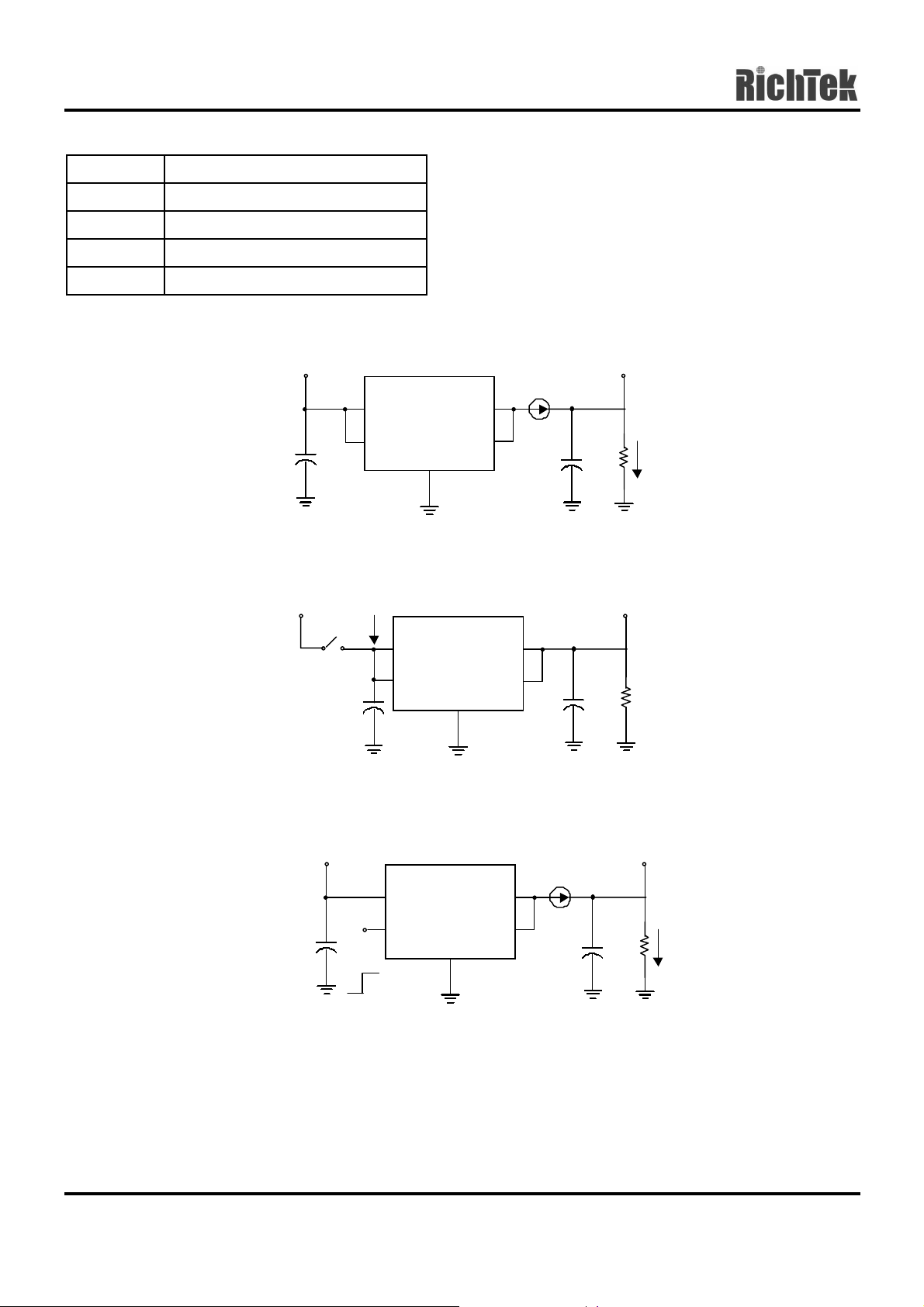
Applications Information
RT9701 CBL
V
IN
C
IN
1µF
C
= 1µF, C
IN
C
= 1µF, C
IN
= 10µF, C
C
IN
VIN
= 470µF (Low ESR) on M/B
OUT
= 330µF (Low ESR) on Notebook
OUT
= 1µF on USB de vice
OUT
VOUT
VOUTVIN
GND
V
OUT1
C
OUT
Fig. 1 High Side Power Swi tch
RT9701 CB
OFF
VIN
CE
GND
VOUT
VOUT
V
C
OUT
V
IN
C
IN
V
CE
ON
Fig. 2 High Side Power Swi tch with Chip Enab le Control
Filtering
To limit the input voltage drop during hot-plug events,
connect a 1µF ceramic capacitor from VIN to GND.
However, higher capacitor values will further reduce
the voltage drop at the input.
Connect a sufficient capacitor from VOUT to GND.
This capacitor helps to prevent inductive parasitics
from pulling VOUT negative during turn-off or EMI
damage to other components during the hot-
detachment. It is also necessary for meeting the USB
specification during hot plug-in operation. If RT9701
is implanted in device end application, minimum 1µF
capacitor from VOUT to GND is recommended and
higher capacitor values are also preferred.
OUT1
V
OUT2
C
OUT
C
OUT
Ferrite beads in series with all power and ground
lines are recommended to eliminate or significantly
reduce EMI. In selecting a ferrite bead, the DC
resistance of the wire used must be kept to a
minimum to reduce the voltage drop.
Reverse current preventing
The output MOSFET and driver circuitry are also
designed to allow the MOSFET source to be
externally forced to a higher voltage than the drain
(VOUT > VIN ≥ 0). To prevent reverse current from
such condition, disable the switch (RT9701CB) or
connect VIN to a fixed voltage under 1.3V.
Layout and Thermal Dissipation
V
OUT2
z Place the switch as close to the USB connector as
possible. Keep all traces as short as possible to
reduce the effect of undesirable parasitic
inductance.
z Place the output capacitor and ferrite beads as
close to the USB connector as possible.
z If ferrite beads are used, use wires with minimum
resistance and large solder pads to minimize
connection resistance.
z If the package is with dual VOUT or VIN pins,
short both the same function pins as Fig.1 or Fig.2
to reduce the internal turn-on resistance. If the
output power will be delivered to two individual
ports, it is specially necessary to short both VOUT
pin at the switch output side in order to protect the
switch when each port are plug-in separately.
z Under normal operating conditions, the package
can dissipate the channel heat away. Wide power-
bus planes connected to VIN and VOUT and a
ground plane in contact with the device will help
dissipate additional heat.
In choosing these capacitors, special attention must
be paid to the Effective Series Resistance, ESR, of
the capacitors to minimize the IR drop across the
capacitor’s ESR. A lower ESR on this capacitor can
get a lower IR drop during the operation.
www.richtek-ic.com.tw DS9701-05 October 2001
10

Package Information
RT9701
D
C
b
A
e
Dimensions In Millimeters Dimensions In Inches
Symbol
A 0.889 1.295 0.035 0.051
A1 0.000 0.152 0.000 0.006
B
A1
Min Max Min Max
H
L
B 1.397 1.803 0.055 0.071
b 0.356 0.559 0.014 0.022
C 2.591 2.997 0.102 0.118
D 2.692 3.099 0.106 0.122
e 0.838 1.041 0.033 0.041
H 0.102 0.254 0.004 0.010
L 0.356 0.610 0.014 0.024
SOT- 25 Surface Mount Package
DS9701-05 October 2001 www.richtek-ic.com.tw
11

RT9701
RICHTEK TECHNOLOGY CORP.
Headquarter
6F, No. 35, Hsintai Road, Chupei City
Hsinchu, Taiwan, R.O.C.
Tel: (8863)5510047 Fax: (8863)5537749
www.richtek-ic.com.tw DS9701-05 October 2001
RICHTEK TECHNOLOGY CORP.
Taipei Office (Marketing)
8F-1, No. 137, Lane 235, Paochiao Road, Hsintien City
Taipei County, Taipei, R.O.C.
Tel: (8862)89191466 Fax: (8862)89191465
Email: marketing@richtek-ic.com.tw
12
 Loading...