

RT9269
Tiny Package, High Efficiency, Constant Current LED Driver
General Description
The RT9269 is a compact, high efficient LED driver with
high flexibility of application conf igurations in charge pump
mode or in boost rectifier mode, delivering Tens of mA
constant output current f or driving 1~4 white LED's.
The 0.25V low reference voltage minimized the power loss
across the current-setting resistor .
The wide applica ble V DD ra nge makes R T9269 suitable for
1 to 4 battery cell applications as well as being supplied
with 2.5/3.3/5/6V system powers. The 500kHz high
switching rate minimized the size of external components.
Besides, the 17μA low quiescent current together with high
efficiency maintains long battery lifetime.
The output current is set with 1 external resistor . And the
chip enable (EN) pin can be used for tuning the LED
brightness by controlling the ON/OFF duty with external
clock. RT9269 is provided in SOT -23-6 pa ckage.
Ordering Information
RT9269
Package Type
E : SOT-23-6
Lead Plating System
P : Pb Free
G : Green (Halogen Free and Pb Free)
Note :
Richtek products are :
` RoHS compliant and compatible with the current require ments of IPC/JEDEC J-STD-020.
` Suitable for use in SnPb or Pb-free soldering processes.
Features
zz
0.25V Low Reference Voltage
z
zz
μμ
zz
z 17
μA Quiescent (Switch-off) Supply Current
zz
μμ
zz
z Zero Shutdown Mode Supply Current
zz
zz
z 85% Efficiency
zz
zz
z 500kHz Fixed Switching Rate
zz
zz
z T uning LED brightness with EN Pin ON/OFF Duty
zz
z Small SOT-23-6 Package
zz
z RoHS Compliant and 100% Lead (Pb)-Free
zz
Applications
z LED Module
z Hand Held Pa nel
z Compact Ba ck Light Module
z Small Battery Charger
z Constant Current Source
Pin Configurations
(TOP VIEW)
FB
VDD LX
4
56
23
EXT
GND
EN
SOT-23-6
Marking Information
For marking information, conta ct our sales representative
directly or through a Richtek distributor located in your
area.
DS9269-12 April 2011 www.richtek.com
1
RT9269
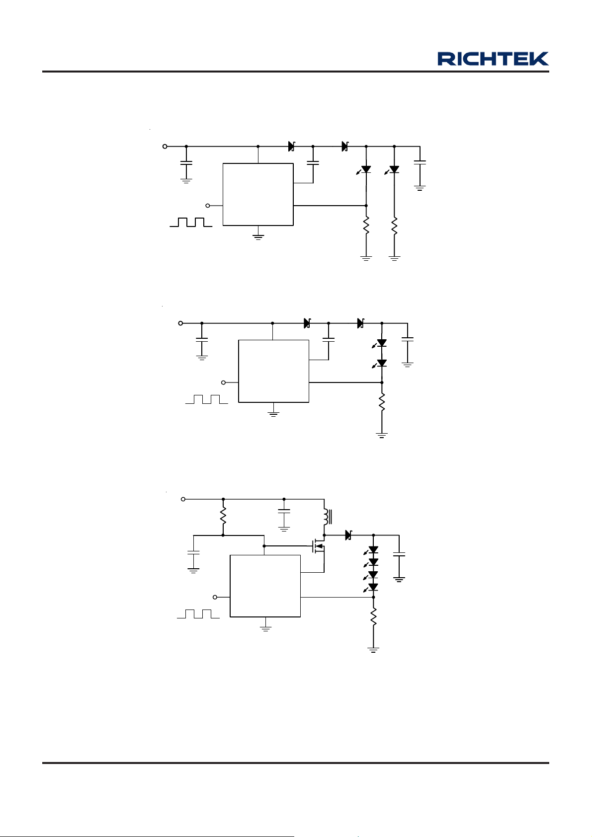
T ypical Application Circuit
V
IN
C1
1uF
To VDD
or
Duty Control
Brightness
Figure 1. RT9269 drives single or parallel LED's in charge pump configuration
V
IN
To VDD
or
Duty Control
Brightness
C1
1uF
VDD
RT9269
GND
RT9269
D1 D2
EXT
0.25V
FBEN
VDD
EXT
FBEN
GND
C2
1uF
D1 D2
C2
1uF
0.25V
C3
1uF
R1 R2
15 15
C3
1uF
R1
15
Figure 2. RT9269 drives 2 series connected LED's in charge pump configuration
V
IN
C1
1uF
To VDD
or
Duty Control
Brightness
R1
1K
VDD
RT9269
GND
C2
10uF
LX
FBEN
0.25V
L1
10uH to 100uH
Q1
C3
10uF
R2
15
Figure 3. RT9269 drives 2~4 series connected LED's in boost rectifier configuration
Note: NICHIA NSCW100 is used for RT9269 LED parts.
2
DS9269-12 April 2011www.richtek.com

Functional Pin Description
RT9269
Pin No. Pin Name
1 EN
2 EXT
3 GND
4 LX
5 VDD
6 FB
Pin Function
Chip Enable (Active High)
Output Pin for Configuring Charge Pump or Driving External NMOS
Ground
Pin for Switching
Input Positive Power Pin of RT9269
Feedback Input pin Internal Reference Voltage for the Error Amplifier is 0.25V.
Function Block Diagram
VDD
FB
1.25V
VDD
RT9269
-
Loop Control Circuit
+
EXT
LX
Q1
N MOS
R1
EN
R2
Q2
N MOS
Over Temp.
Detector
Shut Down
GND
DS9269-12 April 2011 www.richtek.com
3

RT9269
Absolute Maximum Ratings
z Supply V oltage ---------------------------------------------------------------------------------------------------−0.3V to 7V
z LX Pin Switch V oltage ------------------------------------------------------------------------------------------ −0.3V to (V
z Other I/O Pin V oltage s------------------------------------------------------------------------------------------ −0.3V to (V
z LX Pin Switch Current ------------------------------------------------------------------------------------------ 2.5A
z EXT Pin Driver Current ------------------------------------------------------------------------------------------200mA
z Power Dissipation, P
D
@ T
= 25°C
A
SOT-23-6----------------------------------------------------------------------------------------------------------- 0.25W
z Pack age Thermal Resistance
SOT-23-6, θJA----------------------------------------------------------------------------------------------------- 250°C/W
z Operating Junction T emperature------------------------------------------------------------------------------125°C
z Storage T emperature Range----------------------------------------------------------------------------------- −65°C to +150°C
Electrical Characteristics
(VIN =3.3V, VDD set to 5V, Load Current = 0, T
Parameter Symbol Test Conditions Min Typ Max Unit
= 25° C, unless otherwise specified)
A
+0.8V)
DD
+0.3V)
DD
Start-UP Voltage
V
Operating VDD Range VDD
No Load Current I (VIN) I
Switch-off Current I (VDD)
Shutdown Current I (VIN) I
Feedback Reference Voltage
Switching Rate
Maxi mum Du ty
NO LOAD
I
SWITCH V
OFF
V
F
D
LX ON Resistance
Current Limit Setting
EXT ON Resistance to VDD
I
LIMIT
EXT ON Resistance to GND
EN Pin Trip Level
Temperature Stability for V
Thermal Shutdown
Thermal Shutdown Hysterises
T
REF
T
ΔT
I
ST
V
= 1mA
L
p in voltage
V
DD
= 3.3V, V
IN
= 6V
IN
OUT
EN Pin = 0V, VIN = 6V
REF
V
S
MAX
Close Loop, VDD = 5V 0.25 V
= 5V
DD
V
= 5V
DD
V
= 5V
DD
VDD = 5V
VDD = 5V
V
= 5V
DD
V
= 5V
DD
S
SD
SD
-- 50 --
-- 165 --
-- 10 --
= 5V
-- 0.98 1.05 V
2 -- 6.5 V
-- 30 --
μA
-- 17 -- μA
-- 0.1 1
μA
-- 500 -- kHz
-- 75 -- %
-- 0.4 -- Ω
-- 500 --
-- 5 --
-- 5 -- Ω
mA
Ω
0.4 0.8 1.2 V
ppm/°C
°C
°C
DS9269-12 April 2011www.richtek.com
4

Typical Operating Characteristics
RT9269
Efficiency vs. Input Voltage
89
4LEDs, L = 47uH
87
85
83
Efficiency (%)
81
79
600
500
400
300
200
Frequency(kHz) A
100
0
I
= 20mA
OUT
I
= 15mA
OUT
2.533.544.555.56
Input Vol tage (V)
Frequency vs. V
0123456
DD
FB = GND, TA=25°C
VDD (V)
Efficiency vs. V
85
6LEDs, L = 33uH
84
83
I
= 20mA
82
81
Efficiency(%)
80
79
33.544.555.56
OUT
I
OUT
= 15mA
IN
VIN(V)
Efficiency v s. Input Voltage
100
I
= 20mA @VIN > 3.8V
OUT
90
I
80
70
Efficiency (%)
60
50
3 3.5 4 4.5 5 5.5 6
= 15mA
OUT
@VIN >
Refer tp Application Circuit Figure 2
Input Vol tag e (V)
VFB vs. Ambient Temperature
256
254
252
250
VFB (mV)
248
246
244
-40-30-20-100 1020304050607080
Ambient Temperatu re
(°C)
100
90
80
70
60
50
Efficiency (%)
40
30
20
Efficiency vs. Output Current
VIN = 2.7V
VIN = 4.2V
VIN = 3.6V
0.1 1 10 100
Output Current (mA)
DS9269-12 April 2011 www.richtek.com
5

RT9269
V
LX
I
OUT
Power ON Waveform
IN
200mA/Div
I
IN
Refer tp Application Circuit Figure 3
Time (2.5ms/Div)
LX vs. Output Ripple
VIN = 3.0V for 4LEDs
20mA/Div
VIN = 3.0V for 4LEDs
I
OUT
Power ON Waveform
V
IN
LX
200mA/Div
I
IN
20mA/Div
Refer tp Application Circuit Figure 3
Time (2.5ms/Div)
LX vs. Output Ripple
VIN = 2.5V for 4LEDs
VIN = 2.5V for 4LEDs
V
I
OUT
I
OUT
V
EN
OUT
LX
20mA/Div
Refer tp Application Circuit Figure 3
Time (500ns/Div) ((500ns/Div)
Power UP Waveform
IN
LX
20mA/Div
Refer tp Application Circuit Figure 3
V
= 3.0V,I
IN
OUT
= 20mA
V
I
EN
I
OUT
LX
OUT
20mA/Div
OUT
Refer tp Application Circuit Figure 3
Time (1us/Div)
Power UP Waveform
V
IN
LX
20mA/Div
Refer tp Application Circuit Figure 3
V
= 2.5V,I
IN
OUT
= 20mA
Time (250us/Div)
Time (100us/Div)
DS9269-12 April 2011www.richtek.com
6

RT9269
V
I
OUT
V
Power On Waveform
V
= VIN = 3.8V
EN
I
= 20mA
OUT
EN
I
IN
Refer tp Application Circuit Figure 2
Time (10ms/Div)
EN Pin Shutdown Response
LX
V
= 1.25V
EN
VIN = 3.8V
I
= 20mA
OUT
I
Power Up Waveform
V
EN
I
IN
OUT
Refer tp Application Circuit Figure 2
Time (500us/Div)
LX vs. Output Ripple
V
LX
V
= VIN = 3.8V, I
EN
V
= 1.25V
EN
VIN = 3.8V
I
= 20mA
OUT
= 20mA
OUT
I
OUT
I
I
IN
Refer tp Application Circuit Figure 2
Time (500us/Div)
Power On Waveform
V
IN
I
IN
OUT
V
LX
Refer tp Application Circuit Figure 1
V
= VIN = 3.2V
EN
I
= 40mA
OUT
I
OUT
V
I
OUT
V
OUT
Refer tp Application Circuit Figure 2
Time (1us/Div)
Power Up Waveform
V
IN
I
IN
LX
Refer tp Application Circuit Figure 1
V
= 1.2V, VIN = 3.2V
EN
I
= 40mA
OUT
Time (5ms/Div)
Time (250us/Div)
DS9269-12 April 2011 www.richtek.com
7

RT9269
I
OUT
V
EN Pin Shutdown Response
V
IN
V
= 1.2V VIN = 3.2V
EN
I
= 40mA
OUT
I
IN
LX
Refer tp Application Circuit Figure 1
V
IN
I
IN
V
OUT
Refer tp Application Circuit Figure 1
Time (250us/Div)
Brightness Control
V
IN
V
IN
LX vs. Output Ripple
V
= VIN = 3.2V, I
EN
Time (1us/Div)
Brightness Control
OUT
= 40mA
I
OUT
LX
EN
80% Duty
External Signal
VIN = 3.0V
I
= 20mA
OUT
Time (1ms/Div)
I
OUT
LX
EN
80% Duty
External Signal
VIN = 2.5V
I
= 20mA
OUT
Time (1ms/Div)
DS9269-12 April 2011www.richtek.com
8

Outline Dimension
RT9269
H
D
L
C
b
A
e
B
A1
Dimensio ns In Millim eters Dimensions In Inches
Symbol
Min Max Min Max
A 0.889 1.295 0.031 0.051
A1 0.000 0.152 0.000 0.006
B 1.397 1.803 0.055 0.071
b 0.250 0.560 0.010 0.022
C 2.591 2.997 0.102 0.118
D 2.692 3.099 0.106 0.122
e 0.838 1.041 0.033 0.041
H 0.080 0.254 0.003 0.010
L 0.300 0.610 0.012 0.024
SOT-23-6 Surface Mount Package
Richtek Technology Corporation
Headquarter
5F, No. 20, Taiyuen Street, Chupei City
Hsinchu, Taiwan, R.O.C.
Tel: (8863)5526789 Fax: (8863)5526611
Information that is provided by Richtek Technology Corporation is believed to be accurate and reliable. Richtek reserve s the right to make any change in circuit de sign,
specification or other related things if necessary without notice at any time. No third party intellectual property infringement of the applications should be guaranteed
by users when integrating Richtek products into any application. No legal responsibility for any said applications is assumed by Richtek.
DS9269-12 April 2011 www.richtek.com
Richtek Technology Corporation
Taipei Office (Marketing)
5F, No. 95, Minchiuan Road, Hsintien City
Taipei County, Taiwan, R.O.C.
Tel: (8862)86672399 Fax: (8862)86672377
Email: marketing@richtek.com
9

 Loading...